onsemi FDB86363-F085 MOSFET N-Channel PowerTrench
FDB86363-F085
Features
- Typical RDS(on) = 2.0 m at VGS = 10 V, ID = 80 A
- Typical Qg(tot) = 131 nC at VGS = 10 V, ID = 80 A
- UIS Capability
- AEC−Q101 Qualified and PPAP Capable
- This Device is Pb−Free, Halide Free and is RoHS Compliant
Applications
- Automotive Engine Control
- Power Train Management
- Solenoid and Motor Drivers
- Integrated Starter/Alternator
- Primary Switch for 12 V Systems
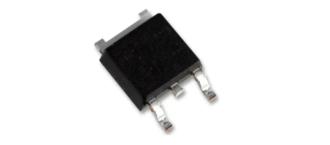
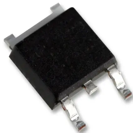
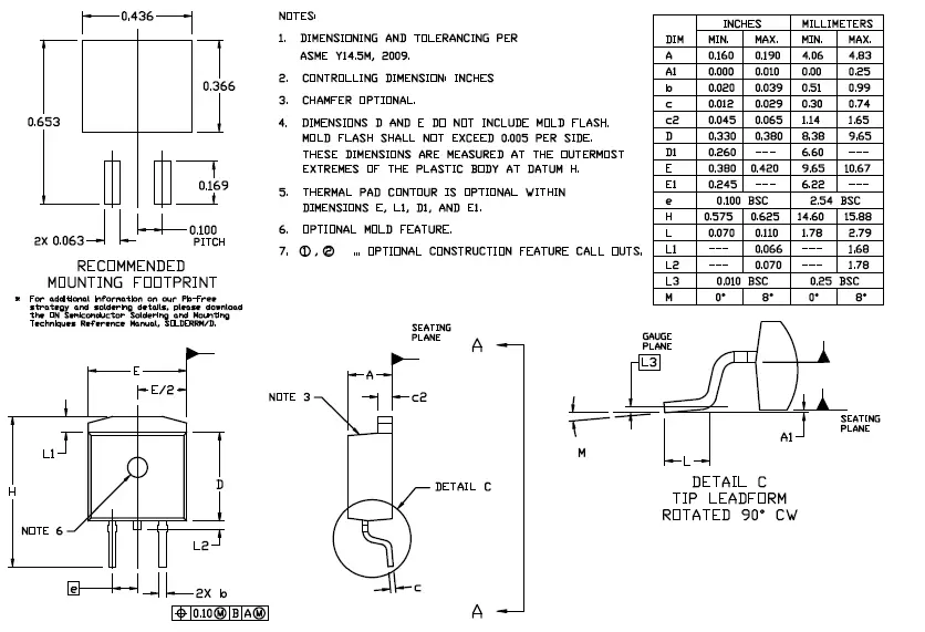
 D2PAK−3 (TO−263, 3−LEAD) CASE 418AJ
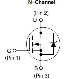
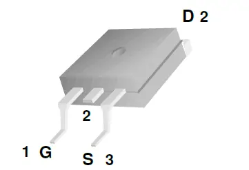
PIN CONFIGURATION
| Position | Designation |
| Pin 1 | Gate |
| Pin 2 / Tab | Drain |
| Pin 3 | Source |
MARKING DIAGRAM
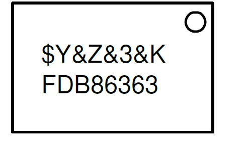 $Y = ON Semiconductor Logo
&Z = Assembly Plant Code
&3 = Numeric Date Code
&K = Lot Code
FDB86363 = Specific Device Code
ORDERING INFORMATION
See detailed ordering and shipping information on page 2 of this data sheet.
MOSFET MAXIMUM RATINGS (TJ = 25°C, Unless otherwise noted)
| Symbol | Parameter | Ratings | Units |
| VDSS | Drain−to−Source Voltage | 80 | V |
| VGS | Gate−to−Source Voltage | ±20 | V |
| ID | Drain Current −Continuous (VGS = 10 V) (Note 1) TC = 25°C | 110 | A |
| −Pulsed TC = 25°C | See Figure 4 | ||
| EAS | Single Pulse Avalanche Energy (Note 2) | 512 | mJ |
| PD | Power Dissipation | 300 | W |
| Derate Above 25°C | 2.0 | W/°C | |
| TJ, TSTG | Operating and Storage Temperature | −55 to +175 | °C |
| RqJC | Thermal Resistance, Junction to Case | 0.5 | ° C/W |
| RqJA | Maximum Thermal Resistance, Junction to Ambient (Note 3) | 43 | ° C/W |
Stresses exceeding those listed in the Maximum Ratings table may damage the device. If any of these limits are exceeded, device functionality should not be assumed, damage may occur and reliability may be affected.
- Current is limited by bondwire configuration.
- Starting TJ = 25°C, L = 0.25 mH, IAS = 64 A, VDD = 80 V during inductor charging and VDD = 0 V during time in avalanche.
- RθJA is the sum of the junction−to−case and case−to−ambient thermal resistance, where the case thermal reference is defined as the solder mounting surface of the drain pins. RθJC is guaranteed by design, while RθJA is determined by the board design. The maximum rating presented here is based on mounting on a 1 in2 pad of 2 oz copper.
PACKAGE MARKING AND ORDERING INFORMATION
| Device Marking | Device | Package | Shipping† |
| FDB86363 | FDB86363−F085 | D2PAK (TO−263) (Pb−Free/Halide Free) | 800 units / Tape & Reel |
†For information on tape and reel specifications, including part orientation and tape sizes, please refer to our Tape and Reel Packaging Specifications Brochure, BRD8011/D
ELECTRICAL CHARACTERISTICS (TJ = 25°C unless otherwise noted)
| Symbol | Parameter | Test Conditions | Min. | Typ. | Max. | Units |
OFF CHARACTERISTICS
| BVDSS | Drain−to−Source Breakdown Voltage | ID = 250 A, VGS = 0 V | 80 | V | ||
| IDSS | Drain−to−Source Leakage Current | VDS = 80 V, VGS = 0 V, TJ = 25°C | 1 | A | ||
| VDS = 80 V, VGS = 0 V, TJ = 175°C (Note 4) | 1 | mA | ||||
| IGSS | Gate−to−Source Leakage Current | VGS = ±20 V | ±100 | nA |
ON CHARACTERISTICS
| VGS(th) | Gate to Source Threshold Voltage | VGS = VDS, ID = 250 A | 2.0 | 3.0 | 4.0 | V |
| RDS(on) | Drain−to−Source On−Resistance | ID = 80 A, VGS = 10 V, TJ = 25°C | 2.0 | 2.4 | mQ | |
| ID = 80 A, VGS = 10 V, TJ = 175°C (Note 4) | 3.8 | 4.3 |
DYNAMIC CHARACTERISTICS
| Ciss | Input Capacitance | VDS = 40 V, VGS = 0 V, f = 1 MHz | 10000 | pF | |||
| Coss | Output Capacitance | 1400 | pF | ||||
| Crss | Reverse Transfer Capacitance | 95 | pF | ||||
| Rg | Gate Resistance | f = 1 MHz | 3.3 | Q | |||
| Qg(TOT) | Total Gate Charge | VGS = 0 V to 10 V | VDD = 64 V, ID = 80 A | 131 | 150 | nC | |
| Qg(th) | Threshold Gate Charge | VGS = 0 V to 2 V | 18 | 21 | nC | ||
| Qgs | Gate−to−Source Gate Charge | 47 | nC | ||||
| Qgd | Gate−to−Drain “Miller” Charge | 24 | nC | ||||
SWITCHING CHARACTERISTICS
| ton | Turn−On Time | VDD = 40 V, ID = 80 A, VGS = 10V, RGEN = 6 Q | 231 | ns | ||
| td(on) | Turn−On Delay | 38 | ns | |||
| tr | Rise Time | 129 | ns | |||
| td(off) | Turn−Off Delay | 64 | ns | |||
| tf | Fall Time | 40 | ns | |||
| toff | Turn−Off Time | 135 | ns |
DRAIN−SOURCE DIODE CHARACTERISTICS
| VSD | Source−to−Drain Diode Voltage | VGS = 0 V, ISD = 80 A VGS = 0 V, ISD = 40 A | 1.25 1.2 | V | ||
| trr | Reverse−Recovery Time | IF = 80 A, 11ISD/11t = 100 A/ s, VDD = 64 V | 88 | 101 | ns | |
| Qrr | Reverse−Recovery Charge | 129 | 157 | nC |
Product parametric performance is indicated in the Electrical Characteristics for the listed test conditions, unless otherwise noted. Product performance may not be indicated by the Electrical Characteristics if operated under different conditions.
- The maximum value is specified by design at TJ = 175°C. Product is not tested to this condition in production.
TYPICAL CHARACTERISTICS
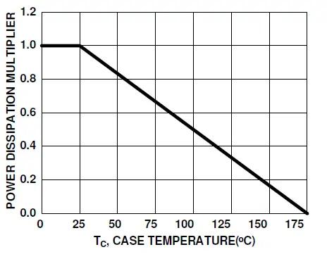 Figure 1. Normalized Power Dissipation vs. Case Temperature
 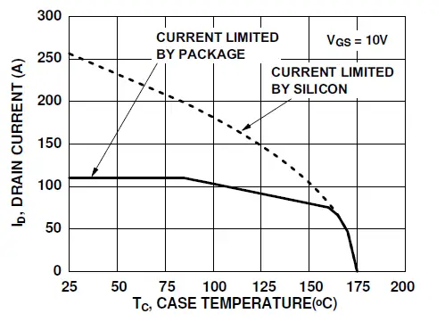 Figure 2. Maximum Continuous Drain Current vs. Case Temperature
 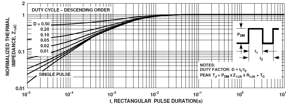 Figure 3. Normalized Maximum Transient Thermal Impedance
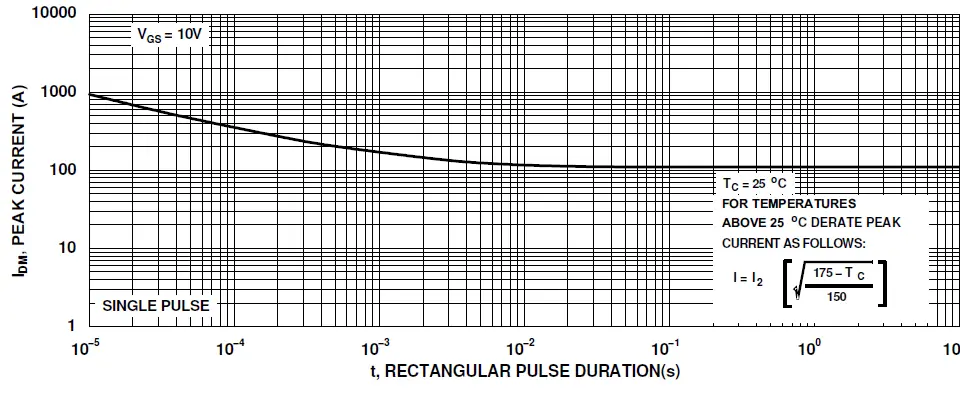 Figure 4. Peak Current Capability
 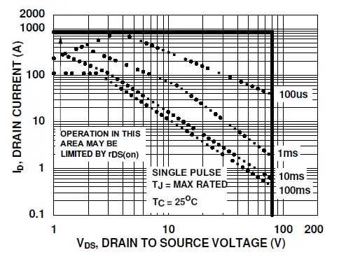 Figure 5. Forward Bias Safe Operating Area
 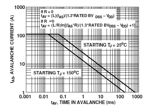 AN7514 and AN7515
Figure 6. Unclamped Inductive Switching Capability 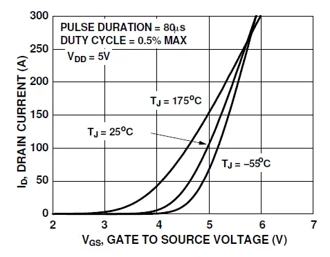 Figure 7. Transfer Characteristics
 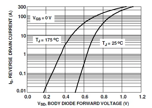 Figure 8. Forward Diode Characteristics
 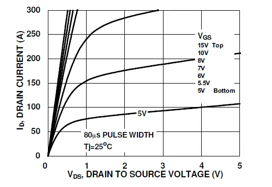 Figure 9. Saturation Characteristics
 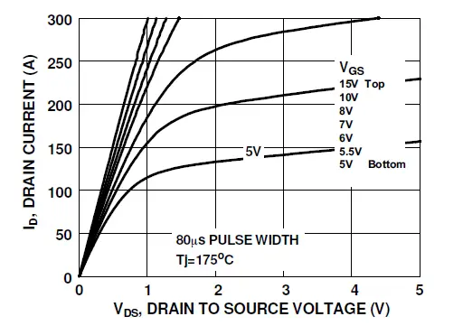 Figure 10. Saturation Characteristics
 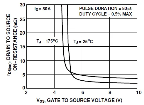 Figure 11. RDSON vs. Gate Voltage
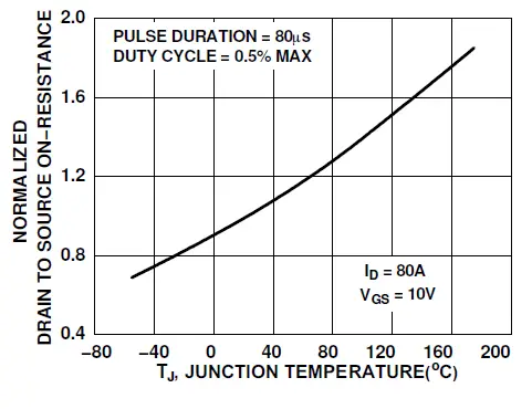 Figure 12. Normalized RDSON vs. Junction
Temperature 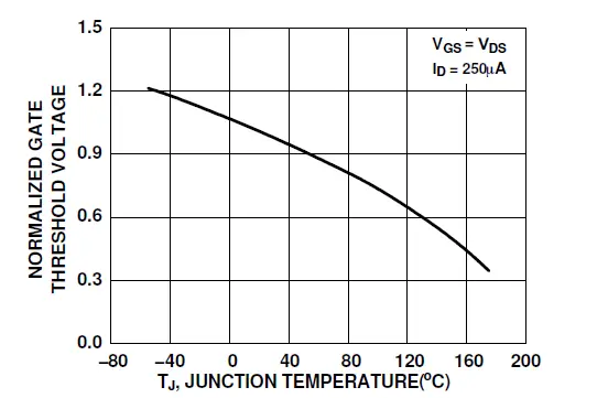 Figure 13. Normalized Gate Threshold Voltage vs. Temperature
 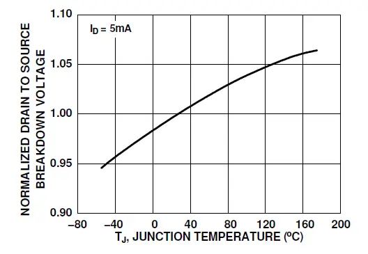 Figure 14. Normalized Drain to Source Breakdown Voltage vs. Junction Temperature
 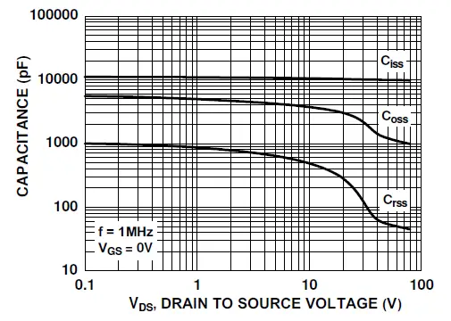 Figure 15. Capacitance vs. Drain to Source Voltage
 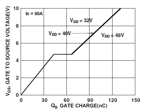 Figure 16. Gate Charge vs. Gate to Source Voltage
D2PAK−3 (TO−263, 3−LEAD)
CASE 418AJ
ISSUE F
SCALE 1:1
DATE 11 MAR 2021
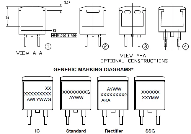
XXXXXX = Specific Device Code
- A = Assembly Location
- WL = Wafer Lot
- Y = Year
- WW = Work Week
- W = Week Code (SSG)
- M = Month Code (SSG)
- G = Pb−Free Package
- AKA = Polarity Indicator
*This information is generic. Please refer to device data sheet for actual part marking. Pb−Free indicator, “G” or microdot “ ”, may or may not be present. Some products may not follow the Generic Marking.
DOCUMENT NUMBER: 98AON56370E Electronic versions are uncontrolled except when accessed directly from the Document Repository. Printed versions are uncontrolled except when stamped “CONTROLLED COPY” in red.
DESCRIPTION: D2PAK−3 (TO−263, 3−LEAD) PAGE 1 OF 1
ON Semiconductor and are trademarks of Semiconductor Components Industries, LLC dba ON Semiconductor or its subsidiaries in the United States and/or other countries. ON Semiconductor reserves the right to make changes without further notice to any products herein. ON Semiconductor makes no warranty, representation or guarantee regarding the suitability of its products for any particular purpose, nor does ON Semiconductor assume any liability arising out of the application or use of any product or circuit, and specifically disclaims any and all liability, including without limitation special, consequential or incidental damages. ON Semiconductor does not convey any license under its patent rights nor the rights of others.
onsemi, , and other names, marks, and brands are registered and/or common law trademarks of Semiconductor Components Industries, LLC dba “onsemi” or its affiliates and/or subsidiaries in the United States and/or other countries. onsemi owns the rights to a number of patents, trademarks, copyrights, trade secrets, and other intellectual property. A listing of onsemi’s product/patent coverage may be accessed at www.onsemi.com/site/pdf/Patent−Marking.pdf. onsemi reserves the right to make changes at any time to any products or information herein, without notice. The information herein is provided “as−is” and onsemi makes no warranty, representation or guarantee regarding the accuracy of the information, product features, availability, functionality, or suitability of its products for any particular purpose, nor does onsemi assume any liability arising out of the application or use of any product or circuit, and specifically disclaims any and all liability, including without limitation special, consequential or incidental damages. Buyer is responsible for its products and applications using onsemi products, including compliance with all laws, regulations and safety requirements or standards, regardless of any support or applications information provided by onsemi. “Typical” parameters which may be provided in onsemi data sheets and/or specifications can and do vary in different applications and actual performance may vary over time. All operating parameters, including “Typicals” must be validated for each customer application by customer’s technical experts. onsemi does not convey any license under any of its intellectual property rights nor the rights of others. onsemi products are not designed, intended, or authorized for use as a critical component in life support systems or any FDA Class 3 medical devices or medical devices with a same or similar classification in a foreign jurisdiction or any devices intended for implantation in the human body. Should Buyer purchase or use onsemi products for any such unintended or unauthorized application, Buyer shall indemnify and hold onsemi and its officers, employees, subsidiaries, affiliates, and distributors harmless against all claims, costs, damages, and expenses, and reasonable attorney fees arising out of, directly or indirectly, any claim of personal injury or death associated with such unintended or unauthorized use, even if such claim alleges that onsemi was negligent regarding the design or manufacture of the part. onsemi is an Equal Opportunity/Affirmative Action Employer. This literature is subject to all applicable copyright laws and is not for resale in any manner.
PUBLICATION ORDERING INFORMATION
LITERATURE FULFILLMENT:
Email Requests to: [email protected]
onsemi Website: www.onsemi.com
TECHNICAL SUPPORT
North American Technical Support:
Voice Mail: 1 800−282−9855 Toll Free USA/Canada Phone: 011 421 33 790 2910
Europe, Middle East and Africa Technical Support:
Phone: 00421 33 790 2910
For additional information, please contact your local Sales Representative


