![]()
![]()
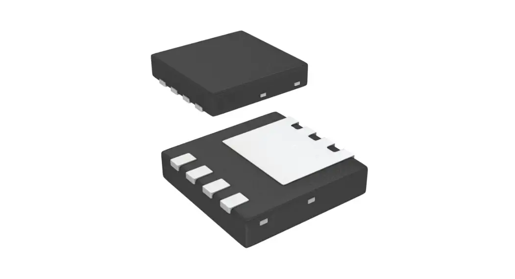
![]() FDBL0200N100 MOSFET N-Channel Power Trench
FDBL0200N100 MOSFET N-Channel Power Trench
Owner’s Manual
www.onsemi.com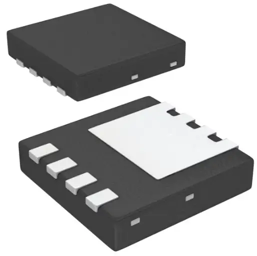
FDBL0200N100 MOSFET N-Channel Power Trench
100 V, 300 A, 2.0 mΩ
FDBL0200N100
Features
- Typical RDS(on) = 1.5 mΩ at VGS = 10 V, ID = 80 A
- Typical Qg(tot) = 95 nC at VGS = 10 V, ID = 80 A
- UIS Capability
- This Device is Pb−Free and is RoHS Compliant
Applications
- Industrial Motor Drive
- Industrial Power Supply
- Industrial Automation
- Battery Operated Tools
- Battery Protection
- Solar Inverters
- UPS and Energy Inverters
- Energy Storage
- Load Switch
| VDSS | RDS(ON) MAX | ID MAX |
| 100 V | 2.0 mΩ @ 10 V | 300 A |
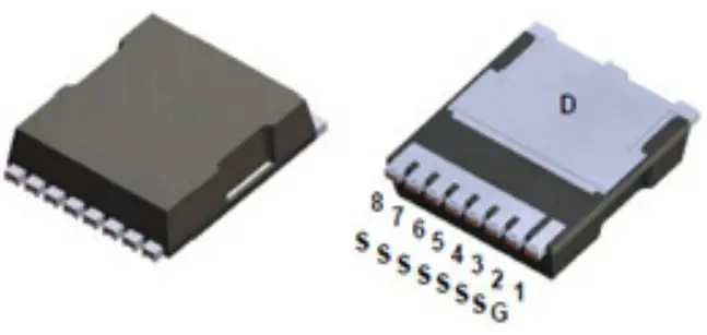 H−PSOF8L 11.68×9.80
CASE 100CU
MARKING DIAGRAM
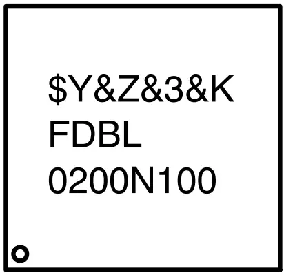
$Y = ON Semiconductor Logo
&Z = Assembly Plant Code
&3 = 3−Digit Plant Code
&K = 2−Digits Lot Run Traceability Code
FDBL0200N100 = Specific Device Code
ORDERING INFORMATION
See detailed ordering and shipping information on page 7 of this data sheet.
FDBL0200N100
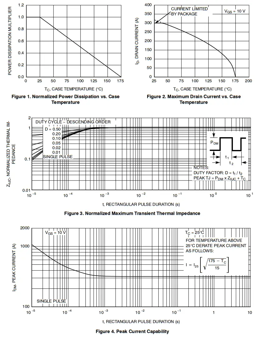
MOSFET MAXIMUM RATINGS (T = 25°C unless otherwise noted)
| Symbol | Rating | Value | Unit | |
| VDSS | Drain−to−Source Voltage | 100 | V | |
| VGS | Gate−to−Source Voltage | ±20 | V | |
| ID | Drain Current − Continuous (VGS = 10) (Note 1) | TC = 25°C | 300 | A |
| Pulsed Drain Current | TC = 25°C | See Figure 4 | ||
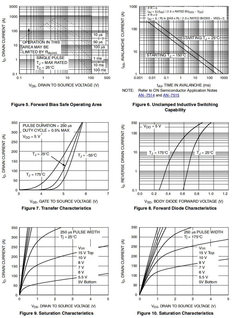
| EAS | Single Pulse Avalanche Energy (Note 2) | 352 | mJ | |
| PD | Power Dissipation | 429 | W | |
| Derate Above 25°C | 2.9 | W/°C | ||
| TJ, TSTG | Operating and Storage Temperature | −55 to +175 | °C | |
| RθJC | Thermal Resistance, Junction to Case (Note 3) | 0.35 | ° C/W | |
| RθJA | Thermal Resistance, Junction to Ambient (Note 3a) | 43 | ° C/W | |
| RθJA | Thermal Resistance, Junction to Ambient (Note 3b) | 62.5 | ° C/W | |
Stresses exceeding those listed in the Maximum Rating table may damage the device. If any of these limits are exceeded, device functionality should not be assumed, damage may occur and reliability may be affected.
- Current is limited by
- Starting TJ = 25°C, L = 1 mH, IAS = 84 A, VDD = 100 V during inductor charging and VDD = 0 V during time in avalanche.
- RθJAis the sum of the junction−to−case and case−to−ambient thermal resistance, where the case thermal reference is defined as the solder mounting surface of the drain RθJC is guaranteed by design, while RθJA is determined by the board design.
- 43°C/W when mounted on a 1 in2 pad of 2 oz copper
- 5°C/W when mounted on a minimum pad of 2 oz copper
ELECTRICAL CHARACTERISTICS (TJ = 25°C unless otherwise noted)
| Symbol | Parameter | Test Condition | Min | Typ | Max | Unit |
OFF CHARACTERISTICS
| BVDSS | Drain−to−Source Breakdown Voltage | ID = 250 µA, VGS = 0 V | 100 | − | − | V | |
| IDSS | Drain−to−Source Leakage Current | VDS = 100 V, VGS = 0V | TJ = 25°C | − | − | 5 | µA |
| TJ = 175°C (Note 4) | − | − | 2 | mA | |||
| IGSS | Gate−to−Source Leakage Current | VGS = ±20V | − | − | ±100 | nA | |
ON CHARACTERISTICS
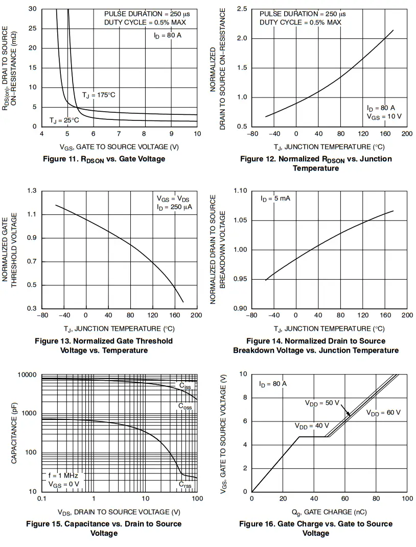
| VGS(th) | Gate to Source Threshold Voltage | VGS = VDS, ID = 250mA | 2.0 | 3.1 | 4.5 | V | |
| RDS(on) | Drain to Source On Resistance | ID = 80A, VGS= 10V | TJ = 25°C | − | 1.5 | 2.0 | mΩ |
| TJ = 175°C (Note 4) | − | 3.3 | 4.3 | mΩ | |||
DYNAMIC CHARACTERISTICS
| Ciss | Input Capacitance | VDS = 50 V, VGS = 0 V, f = 1 MHz | − | 6970 | 9760 | pF |
| Coss | Output Capacitance | − | 3950 | 5530 | pF | |
| Crss | Reverse Transfer Capacitance | − | 29 | 41 | pF | |
| Rg | Gate Resistance | f = 1 MHz | − | 0.45 | 1 | Ω |
| Qg(ToT) | Total Gate Charge at 10 V | VGS = 0 to 10 V, VDD = 80 V, ID = 80 A | − | 95 | 133 | nC |
| Qg(th) | Threshold Gate Charge | VGS = 0 to 2 V, VDD = 80 V, ID = 80 A | − | 13 | − | nC |
| Qgs | Gate−to−Source Gate Charge | VDD = 80 V, ID = 80 A | − | 31 | − | nC |
| Qgd | Gate−to−Drain “Miller“ Charge | − | 20 | − | nC |
SWITCHING CHARACTERISTICS
| ton | Turn−On Time | VDD = 50 V, ID = 80 A, VGS = 10 V, RGEN = 6 Ω | − | − | 73 | ns |
| td(on) | Turn−On Delay | − | 31 | 50 | ns | |
| tr | Rise Time | − | 25 | 40 | ns | |
| td(off) | Turn−Off Delay | − | 36 | 58 | ns | |
| tf | Fall Time | − | 9 | 18 | ns | |
| toff | Turn−Off Time | − | − | 59 | ns |
DRAIN−SOURCE DIODE CHARACTERISTICS
| VSD | Source−to−Drain Diode Voltage | ISD = 80 A, VGS = 0 V | − | − | 1.25 | V |
| ISD = 40 A, VGS = 0 V | − | − | 1.2 | V | ||
| trr | Reverse−Recovery Time | IF = 80 A, USD/DT = 100 A/µs, VDD = 80 V | − | 115 | 184 | ns |
| Qrr | Reverse−Recovery Charge | − | 172 | 273 | nC |
Product parametric performance is indicated in the Electrical Characteristics for the listed test conditions unless otherwise noted. Product performance may not be indicated by the Electrical Characteristics if operated under different conditions
TYPICAL CHARACTERISTICS
ORDERING INFORMATION
| Device | Device Marking | Package Type | Reel Size | Tape Width | Shipping† |
| FDBL0200N100 | FDBL0200N100 | H−PSOF8L 11.68×9.80 (Pb−Free) | 13” | 24 mm | 2000 / Tape & Reel |
†For information on tape and reel specifications, including part orientation and tape sizes, please refer to our Tape and Reel Packaging Specifications Brochure, BRD8011/D.
POWERTRENCH is a registered trademark of Semiconductor Components Industries, LLC (SCILLC) or its subsidiaries in the United States and/or other countries.
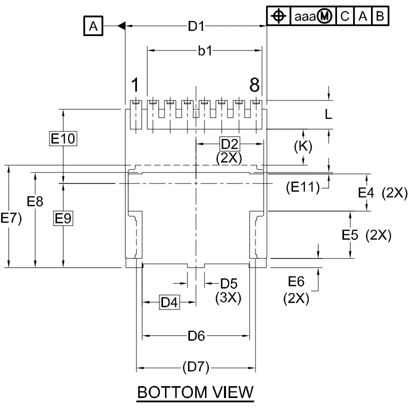
MECHANICAL CASE OUTLINE
PACKAGE DIMENSIONS
H−PSOF8L 11.68×9.80
CASE 100CU ISSUE B
DATE 20 MAY 2022
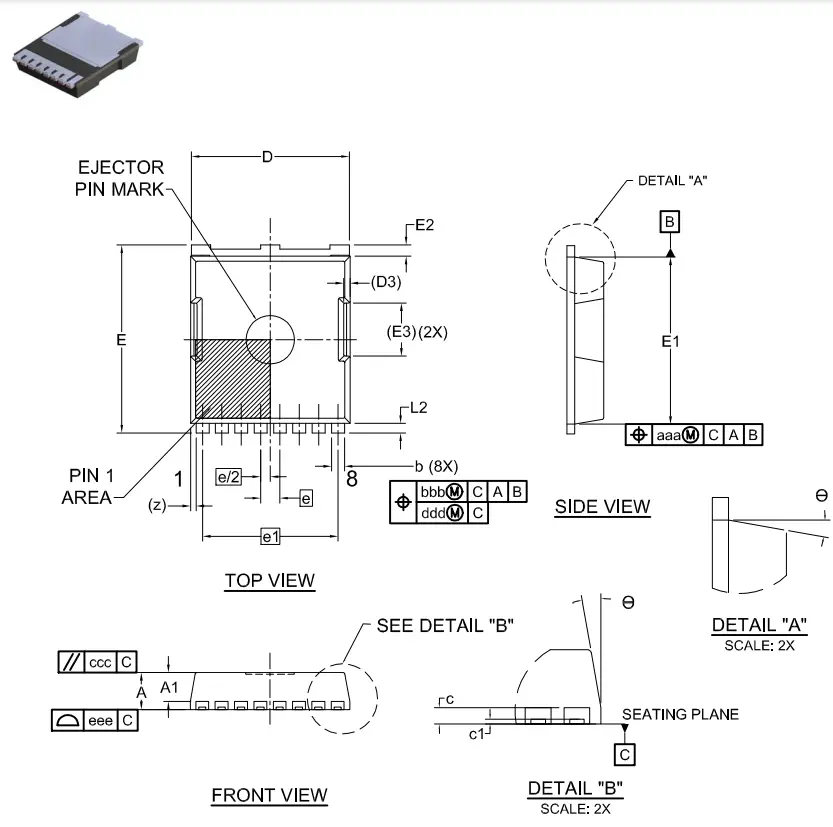
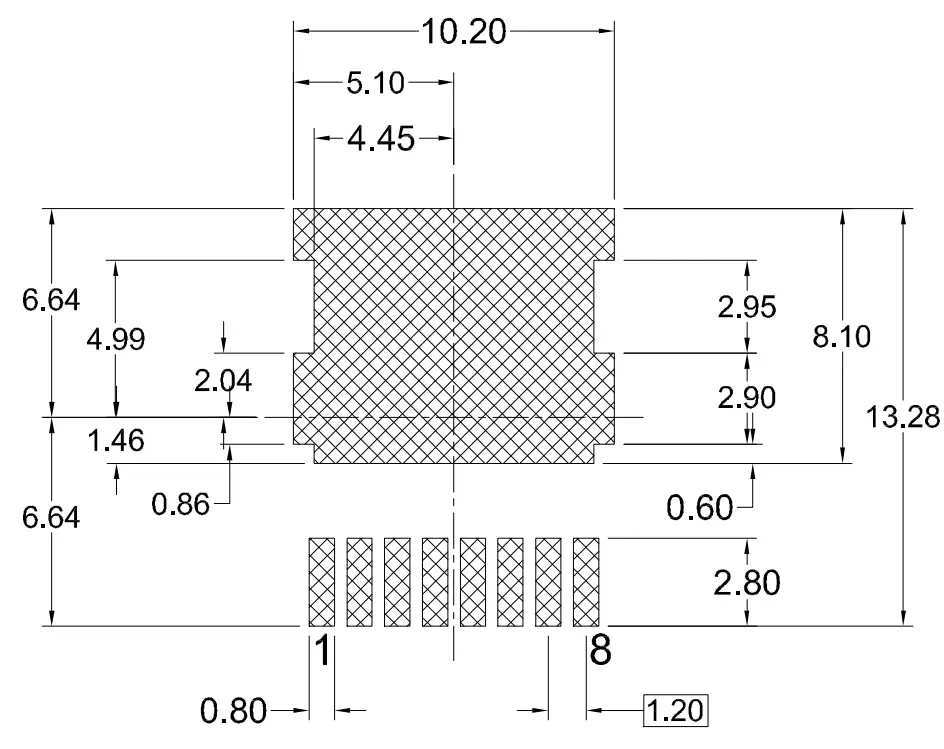
LAND PATTERN RECOMMENDATION
*FOR ADDITIONAL INFORMATION ON OUR PB-FREE STRATEGY AND SOLDERING DETAILS, PLEASE DOWNLOAD THE ON SEMICONDUCTOR SOLDERING AND MOUNTING TECHNIQUES REFERENCE MANUAL, SOLDERRM/D.
NOTES:
1. PACKAGE STANDARD REFERENCE: JEDEC MO-299, ISSUE A.
2. DIMENSIONING AND TOLERANCING PER ASME Y14.5M, 2009.
3. CONTROLLING DIMENSION: MILLIMETERS.
4 COPLANARITY APPLIES TO THE EXPOSED WELL AS THE TERMINALS.
5. DIMENSIONS D1 AND El DO NOT INCLUDE MOLD FLASH, PROTRUSIONS, OR GATE BURRS.
6. SEATING PLANE IS DEFINED BY THE TERMINALS. “Al” IS DEFINED AS THE DISTANCE FROM THE SEATING PLANE TO THE LOWEST POINT ON THE PACKAGE BODY.
| DIM | MILLIMETERS | |||
| MIN. | NOM. | MAX. | ||
| A | 2.20 | 2.30 | 2.40 | |
| Al | 1.70 | 1.80 | 1.90 | |
| b | 0.70 | 0.80 | 0.90 | |
| bl | 8.00 REF | |||
| c | 0.40 | 0.50 | 0.60 | |
| cl | 0.10 | — | — | |
| D | 9.70 | 9.80 | 9.90 | |
| D1 | 9.80 | 9.90 | 10.00 | |
| D2 | 4.73 BSC | |||
| D3 | 0.40 REF | |||
| D4 | 3.75 BSC | |||
| D5 | — | 1.20 | — | |
| D6 | 7.40 | 7.50 | 7.60 | |
| D7 | 8.30 REF | |||
| E | 12. | 12. | 12. | |
| El | 10. | 10. | 10. | |
| E2 | 0.60 | 0.70 | 0.80 | |
| E3 | 3.30 REF | |||
| E4 | — | 2.60 | — | |
| E5 | — | 3.30 | — | |
| DIM | MILLI METERS | ||
| MIN. | I NOM. | I MAX. | |
| E6 | — 0.65 — | ||
| E7 | 7.15 REF | ||
| E8 | 7. | I 6.65 | I 6.75 |
| E9 | 5.89 BSC | ||
| El0 | 5.19 BSC | ||
| Ell | 0.10 REF | ||
| e | 1.20 BSC | ||
| e/2 | 0.60 BSC | ||
| el | 8.40 BSC | ||
| K | 2. | 3. | 3. |
| L | 1.90 | 2.00 | 2.10 |
| 1. | 0.50 | 0.60 | 0.70 |
| z | 0.35 REF | ||
| 9 | 0° | — | 12° |
| aaa | 0.20 | ||
| bbb | 0.25 | ||
| ccc | 0.20 | ||
| ddd | 0.20 | ||
| eee | 0.10 | ||
*This information is generic. Please refer to the device data sheet for actual part marking. Pb−Free indicator, “G” or microdot “ ”, may or may not be present. Some products may not follow the Generic Marking.
GENERIC MARKING DIAGRAM*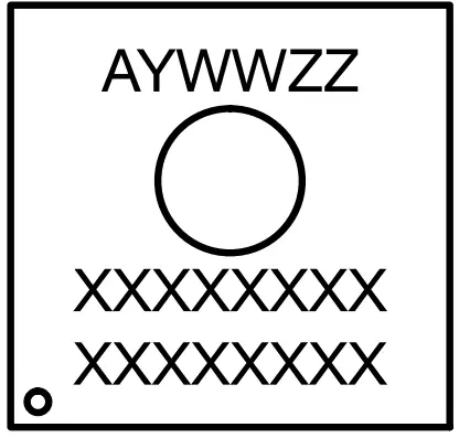 A = Assembly Location
Y = Year
WW = Work Week
ZZ = Assembly Lot Code
XXXX = Specific Device Code
*This information is generic. Please refer to
DOCUMENT NUMBER:98AON13813G
DESCRIPTION: H−PSOF8L 11.68×9.80
Electronic versions are uncontrolled except when accessed directly from the Document Repository.
Printed versions are uncontrolled except when stamped “CONTROLLED COPY” in red.
semi and are trademarks of Semiconductor Components Industries, LLC dba on a semi or its subsidiaries in the United States and/or other countries. onsemi reserves the right to make changes without further notice to any products herein. onsemi makes no warranty, representation or guarantee regarding the suitability of its products for any particular purpose, nor does on semi assume any liability arising out of the application or use of any product or circuit and specifically disclaims any and all liability, including without limitation special, consequential or incidental damages. onsemi does not convey any license under its patent rights nor the rights of others.
© Semiconductor Components Industries, LLC, 2019
www.onsemi.com
semi and other names, marks, and brands are registered and/or common law trademarks of Semiconductor Components Industries, LLC dba “onsemi” or its affiliates
and/or subsidiaries in the United States and/or other countries. onsemi owns the rights to a number of patents, trademarks, copyrights, trade secrets, and other intellectual property.
A listing of on semi’s product/patent coverage may be accessed at www.onsemi.com/site/pdf/Patent−Marking.pdf. onsemi reserves the right to make changes at any time to any products or information herein, without notice. The information herein is provided “as−is” and onsemi makes no warranty, representation or guarantee regarding the accuracy of the information, product features, availability, functionality, or suitability of its products for any particular purpose, nor does onsemi assume any liability arising out of the application or use of any product or circuit, and specifically disclaims any and all liability, including without limitation special, consequential or incidental damages. Buyer is responsible for its products and applications using on semi-products, including compliance with all laws, regulations and safety requirements or standards, regardless of any support or application information provided by on semi. “Typical” parameters which may be provided in onsemi data sheets and/or specifications can and do vary in different applications and actual performance may vary over time. All operating parameters, including “Typicals”, must be validated for each customer application by customer’s technical experts. onsemi does not convey any license under any of its intellectual property rights nor the rights of others. onsemi products are not designed, intended, or authorized for use as a critical component in life support systems or any FDA Class 3 medical devices or medical devices with the same or similar classification in a foreign jurisdiction or any devices intended for implantation in the human bo dy. Should Buyer purchase or use on semi-products for any such unintended or unauthorized application, Buyer shall indemnify and hold onsemi and its officers, employees, subsidiaries, affiliates, and distributors harmless against all claims, costs, damages, and expenses, and reasonable attorney fees arising out of, directly or indirectly, any claim of personal injury or death associated with such unintended or unauthorized use, even if such claim alleges that onsemi was negligent regarding the design or manufacture of the part. onsemi is an Equal Opportunity/Affirmative Action Employer. This literature is subject to all applicable copyright laws and is not for resale in any manner.
PUBLICATION ORDERING INFORMATION
LITERATURE FULFILLMENT:
Email Requests to: [email protected]
Onsemi Website: www.onsemi.com
TECHNICAL SUPPORT
North American Technical Support:
Voice Mail: 1 800−282−9855 Toll-Free USA/Canada
Phone: 011 421 33 790 2910
Europe, Middle East and Africa Technical Support:
Phone: 00421 33 790 2910
For additional information, please contact your local Sales Representative


