ON Semiconductor NCP1653EVB 300 W, Wide Mains, PFC Stage Driven by the NCP1653 Evaluation
Introduction
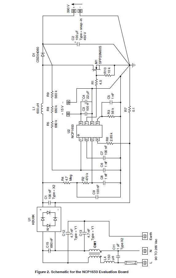
The NCP1653 is a Power Factor Controller to efficiently drive Continuous Conduction Mode (CCM) step-up pre-converters. As shown by the ON Semiconductor application note AND8184/D, that details the four key steps to design a NCP1653 driven PFC stage, this circuit represents a major leap towards compactness and ease of implementation. Housed in a DIP8 or SO−8 package, the circuit minimizes the external components count without sacrificing performance and flexibility. In particular, the NCP1653 integrates all the key protections to build robust PFC stages like an effective input power runaway clamping circuitry. When needed or wished, the NCP1653 also allows operation in Follower Boost mode* to drastically lower the pre-converter size and cost, in a straight-forward manner. For more information on this device, please refer to the ON Semiconductor data sheet NCP1653/D. The board illustrates the circuit capability to effectively drive a high power, universal line application. More specifically, it is designed to meet the following specifications:
specifications
- Maximum output power: 300 W
- Input voltage range: from 90 Vrms to 265 Vrms
- Regulation output voltage: 385 V
- Switching frequency: 100 kHz
This application was tested using a resistive load. As in many applications, the PFC controller is fed by an output of the downstream converter, there is generally no need for an auto-supply circuitry. Hence, in our demo-board, the NCP1653 VCC is to be supplied by a 15 V external power supply. The external voltage source that is to be applied to the NCP1653 VCC, should exceed 13.25 V typically, to allow the circuit startup. After startup, the VCC operating range is from 9.5 to 18 V.
The voltage applied to the NCP1653 VCC must NOT exceed 18 V.
The NCP1653 is a continuous conduction mode and fixed frequency controller (100 kHz). The coil (600 KHZ) is selected to limit the peak-to-peak current ripple in the range of 30% at the sinusoid top, in full load and low line conditions. Again, for details on how the application is designed, please refer to the ON Semiconductor application note AND8184/D. As detailed in the document, the board yields very nice Power Factor ratios and effectively limits the Total Harmonic Distortion (THD).
*The “Follower Boost” mode makes the pre-converter output voltage stabilize at a level that varies linearly versus the AC line amplitude. This technique aims at reducing the difference between the output and input voltages to optimize the boost efficiency and minimize the cost of the PFC stage (refer to MC33260 and NCP1653 data sheet at www.onsemi.com).
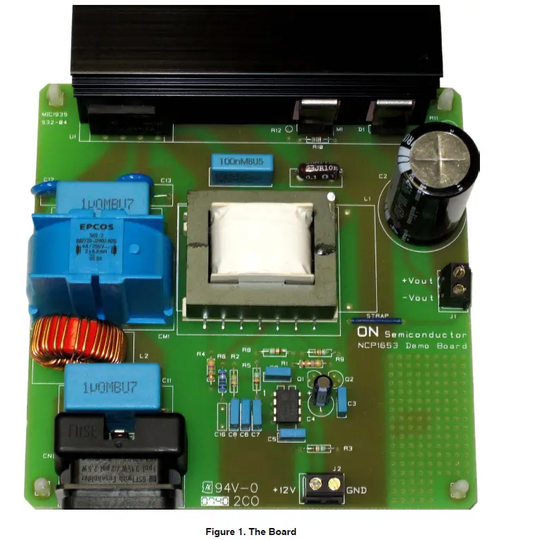
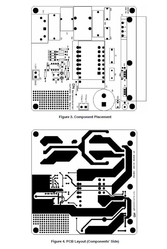
NCP1653EVB
Three coils from three different vendors have been validated on this board
- C1062−B from CoilCraft
- MB09008 from microSpire
- SRW42EC−E02H001 from TDK
For the sake of consistency, this evaluation board reports the performance and results that were obtained using the CoilCraft coil. However, it has been checked that the two other coils yield high performance too.
NCP1653EVB
NCP1653EVB
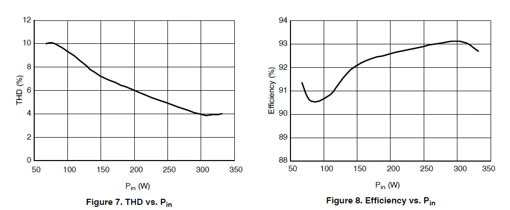
NCP1653EVB GENERAL BEHAVIOR − TYPICAL WAVEFORMS
NCP1653EVB
Table 1. THD AND EFFICIENCY AT Vac = 110 V
| Pin (W) | Vout (V) | Iout (A) | PF (−) | THD (%) | eff (%) |
| 331.3 | 370.0 | 0.83 | 0.998 | 4 | 93 |
| 296.7 | 373.4 | 0.74 | 0.998 | 4 | 93 |
| 157.3 | 381.8 | 0.38 | 0.995 | 7 | 92 |
| 109.8 | 383.5 | 0.26 | 0.993 | 9 | 91 |
| 80.7 | 384.4 | 0.19 | 0.990 | 10 | 91 |
| 67.4 | 385.0 | 0.16 | 0.988 | 10 | 91 |
- The Total Harmonic Distortion keeps below 10% from Pmax (maximum power – 300 W) down to about Pmax/5.
- The efficiency remains higher than 90% for input powers ranging from 67 to 330 W. In standby (no load conditions), the PFC stage enters a stable burst mode, where the circuit keeps regulating the output voltage and minimizes the power consumption (See Figure 11).
NCP1653EVB
Table 2. THD AND EFFICIENCY AT Vac = 220 V
| Pin (W) | Vout (V) | Iout (A) | PF (−) | THD (%) | eff (%) |
| 66.9 | 386.6 | 0.16 | 0.920 | 15 | 92 |
| 80.2 | 386.5 | 0.19 | 0.933 | 14 | 92 |
| 110.0 | 386.7 | 0.27 | 0.960 | 11 | 95 |
| 157.3 | 386.4 | 0.38 | 0.978 | 9 | 93 |
| 215.7 | 386.2 | 0.53 | 0.985 | 8 | 95 |
| 311.4 | 385.4 | 0.77 | 0.989 | 9 | 95 |
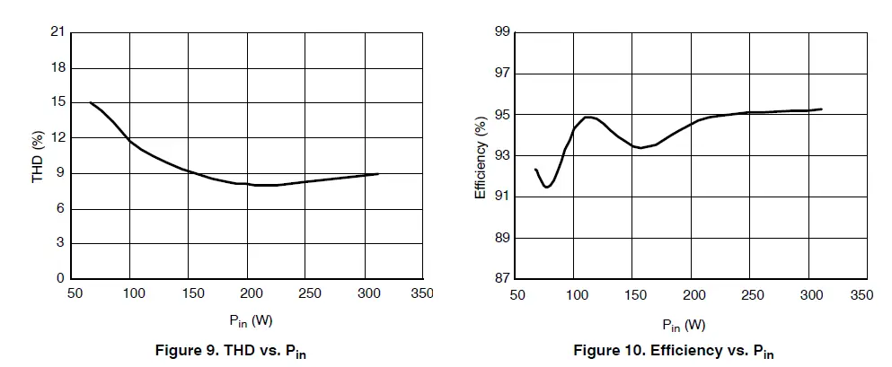
- Similarly to the 110 Vac results, low THD values are obtained. The Total Harmonic Distortion keeps below 15% from Pmax (maximum power – 300 W) down to about Pmax/5.
- Again the efficiency keeps high in a large power range. More specifically, it remains higher than 91% for input powers ranging from 67 to 330 W. In standby (no load conditions), the PFC stage enters a stable burst mode, where the circuit keeps regulating the output voltage and minimizes the power consumption.
NCP1653EVB
Thermal Measurements
The following results were obtained using a thermal camera, after a 1 h operation at 25°C ambient temperature. These data are indicative. They show that the demo-board may require additional heatsink capability if used in high ambient temperature applications.
Measurements Conditions:
- Vac = 90 V
- Pin = 326 W
- Vout = 365 V
- Iout = 0.82 A
- PF = 0.999
- THD = 3%
| Power MOSFET | Heatsink | Bulk Capacitor | Output Diode | Coil (ferrite) | Coil (wires) | Input Bridge |
| 100°C | 80°C | 50°C | 75°C | 100°C | 130°C | 85°C |
No Load Operation
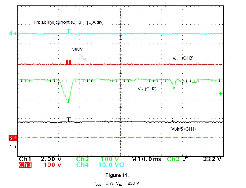
- When in light load, the circuit enters a welcome burst mode that enables the circuit to keep regulating. Vpin5 oscillates around the pin5 internal reference voltage (2.5 V).
- The power losses @ 220 Vac, are nearly 130 mW. This result was obtained by using a W.h meter (measure duration: 1 h).
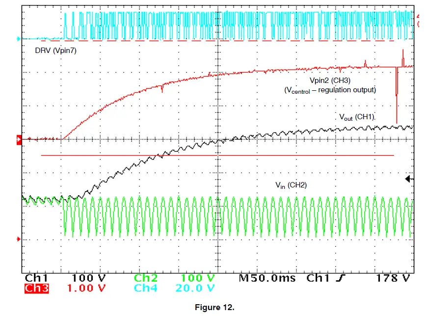
Soft-Start
- The NCP1653 grounds the “Vcontrol” capacitor when it is off, i.e., before each circuit active sequence (“Vcontrol” being the regulation block output). Provided the low regulation
- bandwidth required by PFC stages, “Vcontrol” increases slowly. As a result, the power delivery rises gradually and the PFC pre-regulator startup smoothly and noiselessly.
Test Procedure
- Apply a 500 W/400 W resistive load across the output (between the “+VOUT” and “−VOUT” terminals of the board).
- Adjust a 350 W or more, isolated ac power source so that it outputs a 110 VRMS, sinusoidal voltage (50 or 60 Hz).
- Place a power analyzer able to measure:
- The power delivered by the power source (“Pin”)
- The power factor (“PF”) and the Total Harmonic Distortion (“THD”) of the current absorbed from the ac power source
- Plug the application to the ac power source.
- Supply the controller by applying 15 V to the VCC socket (between the “+12 V” and “GND” terminals of the board) and measure:
Parameters Comments Limits VOUT Voltage Measured between “+VOUT” and “−VOUT” 365 V < VOUT < 385 V PF Power Factor > 0.990 THD Total Harmonic Distortion < 8% Efficiency > 91% - Observe the input current (current drawn from the ac power source) using a current probe and the oscilloscope. The current is nearly sinusoidal.

- Gradually decrease the power source input voltage until the input current top becomes flat. Measure the plateau (see Figure 14). It must be between 4.9 and 5.3 A (over-current limitation). This test must be very short to avoid any excessive heating of the board. Immediately stop the test if the input current exceeds 5.3 A, or if the input voltage is below 75 VRMS).
- Increase the ac power source voltage to 220 V and measure:
Parameters Comments Limits VOUT Voltage Measured between “+VOUT” and “−VOUT” 375 V < VOUT < 395 V PF Power Factor > 0.980 THD Total Harmonic Distortion < 12% Efficiency > 93% - Observe the output voltage (i.e., the voltage between the “+VOUT” and “−VOUT” terminals of the board) with an oscilloscope. Unplug the PFC stage from the power source. Set the triggering level at about 200 V, the trigger position being set at 10% of the screen. Program the scope to observe 50 or 100 ms in single acquisition mode.
- Abruptly apply the power source. Check that the output voltage keeps below 450 V (Over-Voltage Protection) (see Figure 15).
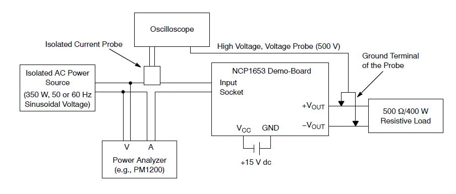
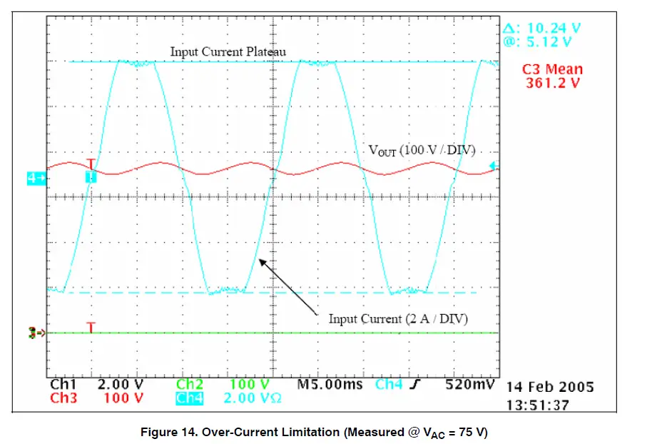
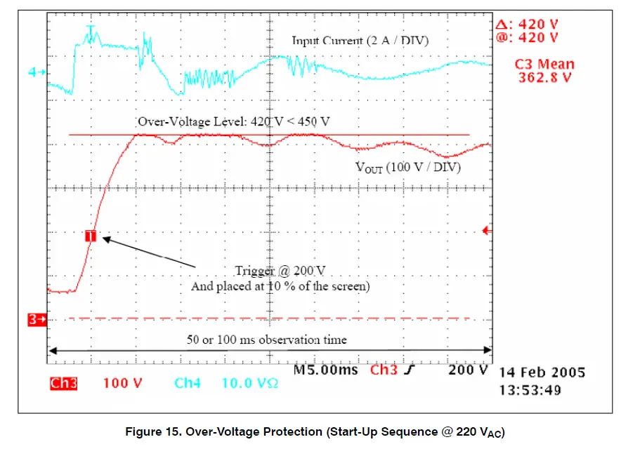
Table 3. BILL OF MATERIALS FOR THE NCP1653 EVALUATION BOARD
| Designator | Qty. | Description | Value | Tolerance | Footprint | Manufacturer | Manufacturer Part Number | Substitution Allowed | Lead Free |
| U2 | 1 | Power Factor Controller | − | − | DIP8 | ON Semiconductor | NCP1653PG | No | Yes |
| C1 | 1 | Class X2 Capacitor | 100 nF, 275 V | 20% | Axial | Evox Rifa | PHE840MX6100M | No | Yes |
| C2 | 1 | Electrolytic Capacitor | 100 µF, 450 V | 20% | Radial | Vishay BC Components | 2222 159 37101 | No | Yes |
| C3, C7, C9 | 3 | Polyester Film Capacitor | 100 nF, 100 V | 10% | Axial | AVX | BQ014E0104K | Yes | Yes |
| C4 | 1 | Electrolytic Capacitor | 47 µF, 35 V | 20% | Radial | Panasonic | ECA1VM470 | Yes | Yes |
| C5, C6, C8 | 3 | Polyester Film Capacitor | 1 nF, 100 V | 10% | Axial | AVX | BQ014E0102K | Yes | Yes |
| C11, C15 | 2 | Class X2 Capacitor | 1 µF, 275 V | 20% | Axial | Evox Rifa | PHE840MD7100M | No | Yes |
| C12, C13 | 2 | Class Y2 Capacitor | 4.7 nF, 250 V | 20% | Disc | Vishay Roederstein | WYO472MCMCF0KR | Yes | Yes |
| R1 | 1 | Axial Resistor | 4.5 Q, 1/4 W | 1% | Axial | Panasonic | ERO−S2PHF4R53 | Yes | Yes |
| R2 | 1 | Axial Resistor | 470 kQ, 1/4 W | 1% | Axial | Vishay Dale | CCF55470KFKE36 | Yes | Yes |
| R3 | 1 | Axial Resistor | 56 kQ, 1/4 W | 1% | Axial | Vishay Dale | CCF5556K0FKE36 | Yes | Yes |
| R4 | 1 | Axial Resistor | 4.7 MQ, 1/4 W | 1% | Axial | Phoenix Passive Comp. | 2306 242 64705 | Yes | Yes |
| R5, R8 | 2 | Axial Resistor | 680 kQ, 1/4 W | 1% | Axial | Vishay Dale | CCF55680KFKE36 | Yes | Yes |
| R6 | 1 | Axial Resistor | 2.8 kQ, 1/4 W | 1% | Axial | Vishay Dale | CCF552K80FKE36 | Yes | Yes |
| R7 | 1 | Axial Resistor | 0.1 Q, 1/4 W | 1% | Axial | Vishay Sfernice | RLP3 0R10 1% | No | Yes |
| R9 | 1 | Axial Resistor | 560 kQ, 1/4 W | 1% | Axial | Vishay Dale | CCF55560KFKE36 | Yes | Yes |
| R10 | 1 | Axial Resistor | 10 kQ, 1/4 W | 1% | Axial | Vishay Dale | CCF5510K0FKE36 | Yes | Yes |
| R12 | 1 | Strap (Short Circuit) | − | − | Through | − | − | Yes | Yes |
| L1 | 1 | PFC Coil | 600 µH | − | − | Coilcraft | C1062−B | No | Yes |
| L4 | 1 | DM Filter | 150 µH, 5 A | 20% | Toroidal | Wurth Elektronik | 7447055 | No | Yes |
| CM1 | 1 | CM Filter | 2´6.8 mH, 4 A | 30% | − | Epcos | B82725J2402N20 | No | Yes |
| U1 | 1 | Bridge Rectifier | 6 A, 800 V | − | KBU | Vishay General Semi. | KBU6K | No | Yes |
| D1 | 1 | Diode | 600 V, 4 A | − | TO220 | Cree | CSD04060A | No | Yes |
| M1 | 1 | MOSFET | 600 V, 20 A | − | TO220 | Infineon | SPP20N60S5 | No | Yes |
| H1 | 1 | Heatsink | 2.9°C/W | − | − | Aavid Thermalloy | KM100−1 | Yes | Yes |
| 4 | Board Supports | − | − | − | Richco | TCBS−8−01 | Yes | Yes | |
| F1 | 1 | Fuse | 250 V, 4 A | − | − | Schurter | FTT 0034.5049 | Yes | Yes |
| 2 | Thermal Pad (TO220) | − | − | − | Bergquist | 3223−07FR−43 | Yes | Yes | |
| 1 | Heatsink Clip (TO218) | − | − | − | Aavid Thermalloy | 4473 | Yes | Yes | |
| 2 | Heatsink Clip (TO220) | − | − | − | Aavid Thermalloy | 4426 | Yes | Yes | |
| CN1 | 1 | AC Connector | − | − | − | Schurter | GSF1.1201.31 | Yes | Yes |
| J1, GND | 2 | Terminal Block | − | − | Pitch: 5mm | Weidmuller | 1715250000 | Yes | Yes |
| 3 | Screws | − | − | − | − | MPMS 003 0008 PH | − | − | |
| STRAP | 1 | Strap (Short Circuit) | − | − | − | 3M | 923345−06−C | Yes | Yes |
Table 4. VENDORS CONTACTS
| Vendor | Contact | Product Information |
| CoilCraft | − | www.coilcraft.com |
| microSpire | − | www.microspire.com |
| TDK | [email protected] | www.tdk.co.jp/tetop01/ |
| EPCOS | − | www.epcos.fr/ |
| CREE | www.cree.com/Products/pwr_sales2.asp | www.cree.com/Products/pwr_index.asp |
onsemi, , and other names, marks, and brands are registered and/or common law trademarks of Semiconductor Components Industries, LLC dba “onsemi” or its affiliates
and/or subsidiaries in the United States and/or other countries. onsemi owns the rights to a number of patents, trademarks, copyrights, trade secrets, and other intellectual property. A listing of onsemi’s product/patent coverage may be accessed at www.onsemi.com/site/pdf/Patent−Marking.pdf. onsemi is an Equal Opportunity/Affirmative Action Employer. This literature is subject to all applicable copyright laws and is not for resale in any manner. The evaluation board/kit (research and development board/kit) (hereinafter the “board”) is not a finished product and is not available for sale to consumers. The board is only intended for research, development, demonstration and evaluation purposes and will only be used in laboratory/development areas by persons with an engineering/technical training and familiar with the risks associated with handling electrical/mechanical components, systems and subsystems. This person assumes full responsibility/liability for proper and safe handling. Any other use, resale or redistribution for any other purpose is strictly prohibited. THE BOARD IS PROVIDED BY ONSEMI TO YOU “AS IS” AND WITHOUT ANY REPRESENTATIONS OR WARRANTIES WHATSOEVER. WITHOUT LIMITING THE FOREGOING, ONSEMI (AND ITS LICENSORS/SUPPLIERS) HEREBY DISCLAIMS ANY AND ALL REPRESENTATIONS AND WARRANTIES IN RELATION TO THE BOARD, ANY MODIFICATIONS, OR THIS AGREEMENT, WHETHER EXPRESS, IMPLIED, STATUTORY OR OTHERWISE, INCLUDING WITHOUT LIMITATION ANY AND ALL REPRESENTATIONS AND WARRANTIES OF MERCHANTABILITY, FITNESS FOR A PARTICULAR PURPOSE, TITLE, NON−INFRINGEMENT, AND THOSE ARISING FROM A COURSE OF DEALING, TRADE USAGE, TRADE CUSTOM OR TRADE PRACTICE. onsemi reserves the right to make changes without further notice to any board. You are responsible for determining whether the board will be suitable for your intended use or application or will achieve your intended results. Prior to using or distributing any systems that have been evaluated, designed or tested using the board, you agree to test and validate your design to confirm the functionality for your application. Any technical, applications or
design information or advice, quality characterization, reliability data or other services provided by onsemi shall not constitute any representation or warranty by onsemi, and no additional obligations or liabilities shall arise from onsemi having provided such information or services. onsemi products including the boards are not designed, intended, or authorized for use in life support systems, or any FDA Class 3 medical devices or medical devices with a similar or equivalent classification in a foreign jurisdiction, or any devices intended for implantation in the human body. You agree to indemnify, defend and hold harmless onsemi, its directors, officers, employees, representatives, agents, subsidiaries, affiliates, distributors, and assigns, against any and all liabilities, losses, costs, damages, judgments, and expenses, arising out of any claim, demand, investigation, lawsuit, regulatory action or cause of action arising out of or associated with any unauthorized use, even if such claim alleges that onsemi was negligent regarding the design or manufacture of any products and/or the board. This evaluation board/kit does not fall within the scope of the European Union directives regarding electromagnetic compatibility, restricted substances (RoHS), recycling (WEEE), FCC, CE or UL, and may not meet the technical requirements of these or other related directives.
FCC WARNING – This evaluation board/kit is intended for use for engineering development, demonstration, or evaluation purposes only and is not considered by onsemi to be a finished end product fit for general consumer use. It may generate, use, or radiate radio frequency energy and has not been tested for compliance with the limits of computing devices pursuant to part 15 of FCC rules, which are designed to provide reasonable protection against radio frequency interference. Operation of this equipment may cause interference with radio communications, in which case the user shall be responsible, at its expense, to take whatever measures may be required to correct this interference.
onsemi does not convey any license under its patent rights nor the rights of others. LIMITATIONS OF LIABILITY: onsemi shall not be liable for any special, consequential, incidental, indirect or punitive damages, including, but not limited to the costs of prequalification, delay, loss of profits or goodwill, arising out of or in connection with the board, even if onsemi is advised of the possibility of such damages. In no event shall onsemi’s aggregate liability from any obligation arising out of or in connection with the board, under any theory of liability, exceed the purchase price paid for the board, if any. The board is provided to you subject to the license and other terms per onsemi’s standard terms and conditions of sale. For more information and documentation, please visit
PUBLICATION ORDERING INFORMATION
LITERATURE FULFILLMENT: Email Requests to: [email protected] onsemi Website: www.onsemi.com TECHNICAL SUPPORT North American Technical Support: Voice Mail: 1 800−282−9855 Toll Free USA/Canada Phone: 011 421 33 790 2910 Europe, Middle East and Africa Technical Support: Phone: 00421 33 790 2910 For additional information, please contact your local Sales Representative


