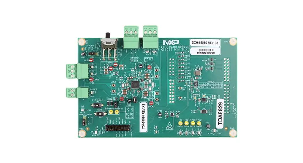
![]() Semiconductors PCA9451A-EVK Evaluation Board
Semiconductors PCA9451A-EVK Evaluation Board
User Manual
Document information
| Information | Content |
| Keywords | PCA9451A, PMIC, i.Mx93x |
| Abstract | This document describes the operation of the PCA9451A-EVK evaluation board |
Revision history
| Rev | Date | Description |
| v.1.0 | 20230330 | Initial version |
Important notice
For engineering development or evaluation purposes only![]() NXP provides the product under the following conditions:
NXP provides the product under the following conditions:
This evaluation kit is for use of ENGINEERING DEVELOPMENT OR EVALUATION PURPOSES ONLY.
It is provided as a sample IC pre-soldered to a printed-circuit board to make it easier to access inputs, outputs and supply terminals. This evaluation board may be used with any development system or other source of I/O signals by connecting it to the host MCU computer board via off-the-shelf cables. This evaluation board is not a Reference Design and is not intended to represent a final design recommendation for any particular application. Final device in an application heavily depends on proper printed-circuit board layout and heat sinking design as well as attention to supply filtering, transient suppression, and I/O signal quality.
The product provided may not be complete in terms of required design, marketing, and or manufacturing related protective considerations, including product safety measures typically found in the end device incorporating the product. Due to the open construction of the product, it is the responsibility of the user to take all appropriate precautions for electric discharge. In order to minimize risks associated with the customers’ applications, adequate design and operating safeguards must be provided by the customer to minimize inherent or procedural hazards. For any safety concerns, contact NXP sales and technical support services.
Introduction
The PCA9451A is a single chip Power Management IC (PMIC) designed to support the i.Mx 93x processors family in both 1 cell Li-ion and Li-polymer battery portable application and 5 V adapter non-portable applications.
This document is the user manual for the PCA9451A evaluation kit. It is intended for the engineers involved in the evaluation, design, implementation, and validation of this single power management-integrated circuit PCA9451A.
The PCA9451A-EVK user manual covers information regarding connecting the hardware, installing the software and tools, configuring the environment and using the kit.
This customer evaluation board provides full access to all the features in the PCA9451A device.
PCA9451A key features
- Six high-efficiency step-down regulators
– One 4 A dual phase buck regulator with DVS feature and remote sense
– One 2 A buck regulator with DVS feature and remote sense
– One 3 A buck regulator
– One 2 A buck regulator
– One 1.5 A buck regulator - Three linear regulators
– One 10 mA LDO
– One 150 mA LDO
– One 200 mA LDO - 400 mA load switch with built-in active discharge resistor
- 32.768 kHz crystal oscillator driver and buffer output
- Two channel logic level translator
- Power control I/O
– Power ON/OFF control
– Standby/run mode control - Fm+ 1 MHz I2 C-bus interface
- ESD protection
– Human Body Model (HBM): +/- 2000 V
– Charged Device Model (CDM): +/-500 V - 7 mm x 7 mm, 56-pin HVQFN with 0.4 mm pitch
Applications
- IoT devices
- Tablet
- Electronic Point of Sale (epos)
- Industrial application
- Monitoring system
- Infotainment
Finding kit resources and information on the NXP website
NXP Semiconductors provides online resources for evaluation boards and its supported device(s) on http://www.nxp.com.
The information page for evaluation boards is http://www.nxp.com/PCA9451A-EVK.
The information page provides overview information, documentation, software and tools, parametric, ordering information and a Getting Started tab. The Getting Started tab provides quick-reference information applicable to these evaluation boards, including the downloadable assets referenced in this document.
4.1 Collaborate in the NXP community
The NXP community is for sharing ideas and tips, asking and answering technical questions, and receiving input on just about any embedded design topic. The NXP community is at http://community.nxp.com.
Getting ready
Working with this evaluation board requires the evaluation kit components, additional hardware, and a Windows PC workstation with installed software.
5.1 Evaluation kit components
- 1x PCA9451A evaluation board, which allows easy evaluation on function and features
- 1x Interface (FTDI C232HM-DDHSL-0) cable, which serves as a USB to I C interface between the computer and the PCA9451A evaluation board.
5.2 Additional hardware
In addition to the kit components, the following hardware is necessary or beneficial when working with this kit.
- Power supply with a range of 3.0 V to 5.0 V and a current limit set initially to 1.0 A (maximum current consumption can be up to 7.0 A)
- Oscilloscope/multimeter
- Electronic load (optional) – each power rail output can be connected to e-load for testing
5.3 Windows PC workstation
This evaluation board requires a Windows PC workstation. Meeting these minimum specifications should produce great results when working with this evaluation board.
- USB-enabled computer with Windows 7, Windows 8, or Windows 10
5.4 PCA9451A-EVK GUI software
Installing software is necessary to work with this evaluation board.
- Go to http://www.nxp.com/PCA9451A-EVK.
- Extract the zip file PCA9451_EVB_GUI.zip into selected folder. No need to install. (if password is asked during unzip, then type “NXP”)
- Install the FTDI cable driver from website https://www.ftdichip.com/Drivers/D2XX.htm
- Run the file PCA9451.exe. The interface window is shown in Figure 1.
Getting to know the hardware
The NXP analog product development boards provide an easy-to-use platform for evaluating NXP products. The boards support a range of analog, mixed-signal, and power solutions. They incorporate monolithic integrated circuits and system-in-package devices that use proven high-volume technology. NXP products offer longer battery life, a smaller form factor, reduced component counts, lower cost, and improved performance in powering state-of-the-art systems.
6.1 Kit overview
This evaluation board features the PCA9451A power management IC. The kit integrates all hardware needed to fully evaluate the PMIC. It integrates a communication bridge based on FTDI to interface with the PCA9451A GUI software interface to fully configure and control the PMIC.
6.1.1 Evaluation board features
- Six buck regulators
– One 4 A buck regulator with DVS
– One 2 A buck regulator with DVS
– One 3 A buck regulator
– One 2 A buck regulator
– One 1.5 A buck regulator - Three linear regulators
– One 10 mA LDO
– One 150 mA LDO
– One 200 mA LDO - 400 mA load switch with a built-in active discharge resistor
- 32.768 kHz crystal oscillator driver and buffer output
- Two-channel logic level translator
- System features
– 2.85 V to 5.5 V operating input voltage range
– Power ON/OFF control
– Standby/run mode control
– Smart DVS control
– Interrupt configuration
– FM+ 1 MHz2 I2 C Interface (via FTDI USB to I C cable)
6.2 Kit featured components
Figure 2 helps to identify the different main components on the board.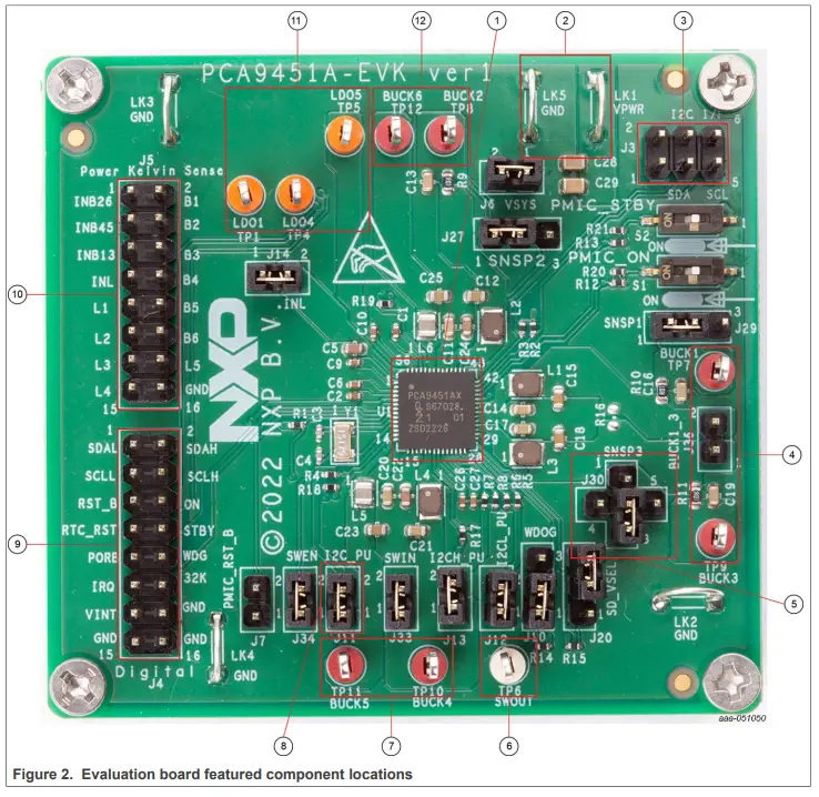
- PCA9451A PMIC
- VPWR and GND input power connectors
- I 2 C connector
- BUCK1 and BUCK3 output test points
- BUCK3 Feedback connection
- Load switch output test point
- BUCK4 and BUCK5 output test points
- I2 C pullup voltage jumper (I2C_PU)
- Digital IO connector
- Kelvin sense connector
- LDO outputs test points
- BUCK2 and BUCK6 output test points
6.3 Default jumper configuration
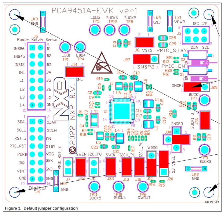 Table 1. Evaluation board jumper description
| Name | Default | Description |
| J6 | 1-2 | Connects PMIC VSYS pin to main board VSYS |
| J7 | No connection | Controls PMIC_RST_B (PMIC Reset) signal • Once it is asserted low (J7 = 1-2), PMIC performs reset. |
| Name | Default | Description |
| J10 | 1-2 | Controls WDOG_B (Watchdog reset input) signal • 1-2 -> Pull-up to VPWR (normal operation) • 2-3 -> Pull-down to GND |
| J11 | 1-2 | Pull up of SDA,SCL, IRQ_B pins to BUCK5. Note: REMOVE JUMPER FOR USE WITH FTDI CABLE AND GUI |
| J12 | 1-2 | Pull up of SCLL,SDAL pins to BUCK5 |
| J13 | 1-2 | Pull up of SCLH,SDAH pins to BUCK4 |
| J14 | 1-2 | INL1 Enablement. Connects the INL input for LDOs to VPWR |
| J20 | 2-3 | Selects SD_VSEL level • 1-2 -> SD_VSEL = High (LDO5 = 1.8 V default output) • 2-3 -> SD_VSEL = Low (LDO5 = 3.3 V default output) |
| J27 | 1-2 | BUCK2 Feedback connection: • 1-2 -> Remote sense • 2-3 -> Local sense |
| J29 | 1-2 | BUCK1 Feedback connection: • 1-2 -> Remote sense • 2-3 -> Local sense |
| J30 | 2-5 | BUCK3 Feedback connection and BUCK1/BUCK3 Dual Phase control: • 1-2 -> Local sense for BUCK3 • 2-3 -> Remote sense for BUCK3 • 2-4 -> Pull-up to INB13 (VPWR rail), BUCK 3 is disabled. • 2-5 -> Pull-down to GND, BUCK1 and BUCK3 are configured as dual phase buck. Note: MAKE SURE J30 IS SET TO 2-5 FOR DUAL-PHASE CONFIGURATION. SOME BOARDS CAME WITH J30=2-3 BY DEFAULT |
| J33 | 1-2 | SWIN Connect to BUCK4 |
| J34 | 1-2 | SW_EN connect to BUCK4 |
| J36 | 1-2 | BUCK1 and BUCK3 Single/Dual Phase • 1-2 -> Dual Phase configuration • No connection -> Single Phase configuration Note: SOME BOARDS CAME WITH J36 OPEN BY DEFAULT, MAKE SURE J36 IS SET TO 1-2 FOR DUAL PHASE CONFIGURATION |
6.4 Test points
Use the test points to measure the output voltage signal of the PMIC regulators and load switch by oscilloscope/ multimeter.
Table 2. Evaluation board test point descriptions
| Name | Signal | Description |
| TP1 | LDO1 | Power path for the LDO1 output. |
| TP4 | LDO4 | Power path for the LDO4 output. |
| TP5 | LDO5 | Power path for the LDO5 output. |
| TP6 | SWOUT | Output of the Load Switch |
Table 2. Evaluation board test point descriptions…continued
| Name | Signal | Description |
| TP7 | BUCK1 | Power path for the BUCK1 output. |
| TP8 | BUCK2 | Power path for the BUCK2 output. |
| TP9 | BUCK3 | Power path for the BUCK3 output. |
| TP10 | BUCK4 | Power path for the BUCK4 output. |
| TP11 | BUCK5 | Power path for the BUCK5 output. |
| TP12 | BUCK6 | Power path for the BUCK6 output. |
6.5 Connectors
6.5.1 Main input power connectors
Main input power VPWR is supplied using LK1 and LK5 connectors.
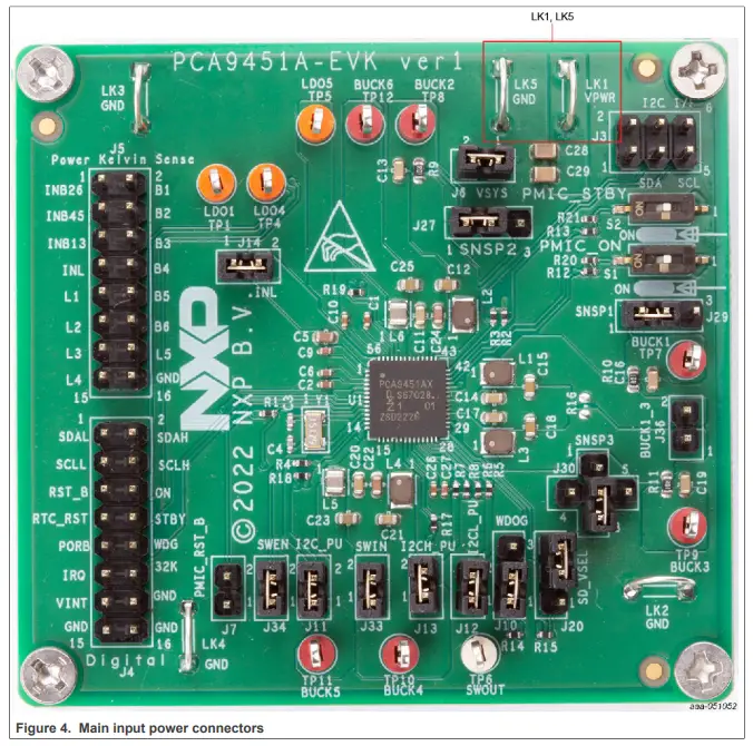 Table 3. Main input power connectors
| Name | Signal | Description |
| LK1 | VPWR | Main system input power supply System operating range from 2.85 V to 5.5 V (5.0 V Typ) |
| LK5 | GND | Main system ground |
6.5.2 Interface connectors
Digital IO connector (J4) is used to have access for easy monitoring of some of the analog and digital pins of the PCA9451A. Table 4 explains each of the pins included in this connector.
Table 4. Digital IO connector (J4)
| Name | Signal | Type | Description |
| J4-1 | SDAL | Input/output | Level translator low voltage IO pin, SDA referenced to VINT, 1.8 V |
| J4-2 | SDAH | Input/output | Level translator high voltage IO pin, SDA referenced to SWIN, 3.3 V |
| J4-3 | SCLL | Output | Level translator low voltage IO pin, SCL referenced to VINT, 1.8 V |
| J4-4 | SCLH | Output | Level translator high voltage IO pin, SCL referenced to SWIN, 3.3 V |
| J4-5 | RST_B | Input | PMIC reset input pin. |
| J4-6 | ON | Input | PMIC ON input from Application processor. |
| J4-7 | RTC-RST | Output | Reset output pin. |
| J4-8 | STBY | Input | Standby mode input from Application processor. |
| J4-9 | PORB | Output | Power On reset output pin. |
| J4-10 | WDG | Input | Active low watchdog reset input pin from application processor. |
| J4-11 | IRQ | Output | Direct connection to IRQ_B pin for interrupt signal |
| J4-12 | 32K | Output | 32.768kHz clock CMOS output with LDO1 power rail. |
| J4-13 | VINT | Power | Internal Power supply output pin. |
| J4-14 | GND | GND | Analog ground. |
| J4-15 | |||
| J4-16 |
I² C connector (J3) is used to interface the PMIC with external I2 C controllers. This connector is typically used to interface the PCA9451A-EVK with the external FTDI cable, for proper communication with the PCA9451A-GUI.
Table 5. I C connector (J3)
| Name | Signal | Type | Description |
| J3-1 | I2C PU | Power | Voltage connection for the interface Pull-up resistors |
| J3-2 | GND | Power | Direct connection to system ground |
| J3-3 | SDA | Input/output | Connection to I2C serial data signal |
| J3-4 | SDA | Input/output | Connection to I2C serial data signal |
| J3-5 | SCL | Input | Connection to I2C serial clock signal |
| J3-6 | GND | Power | Direct connection to system ground |
Kelvin sense connector (J5) is used to have access for easy monitoring of some of the voltage rails of the PMIC. Kelvin measurement makes it possible to accurately measure voltages while eliminating the inherent resistance of the PCB traces.
Table 6. Kelvin sense connector (J5)
| Name | Signal | Description |
| J5-1 | VPWR | Sense from INB26 |
| J5-2 | R_SNSP1 | Remote sense for BUCK1 regulator output |
| J5-3 | VPWR | Sense from INB45 |
| J5-4 | R_SNSP2 | Remote sense for BUCK2 regulator output |
| J5-5 | VPWR | Sense from INB13 |
| Name | Signal | Description |
| J5-6 | R_SNSP2 | Remote sense for BUCK3 regulator output |
| J5-7 | INL1 | Sense from LDO inputs |
| J5-8 | BUCK4FB | Remote sense for BUCK4 regulator output |
| J5-9 | LDO1 | LDO1 sense from LDO load caps |
| J5-10 | BUCK5FB | Remote sense for BUCK5 regulator output |
| J5-12 | BUCK6FB | Remote sense for BUCK6 regulator output |
| J5-14 | LDO5 | LDO5 sense from LDO load caps |
| J5-15 | LDO4 | LDO4 sense from LDO load caps |
| J5-16 | GND | Direct connection to system ground |
Evaluation kit connections and configuration
7.1 Test setup
Figure 5 shows test setup block diagram.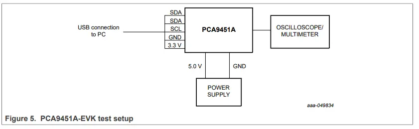 7.2 Evaluation board connection
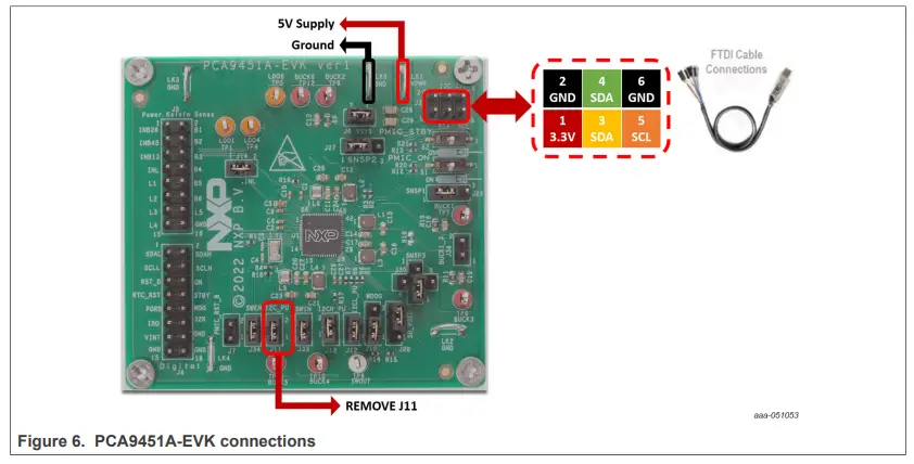 7.2.1 Configure and power the board
Connect the wires of the FTDI cable on the following pins as shown in Figure 6, and make sure the power supply is turned off and the USB connector is disconnected during the wiring stage:
- Connect both SDAs, SCL, GND, and the 3.3 V wires from the FTDI cable as mentioned in Figure 6 above. a. SCL serial clock signal (orange cable) should be connected to pin 5 of the ‘Digital IO’ connector (J3).
b. Both SDA serial data wires (yellow and green cables) should be connected to create bidirectional data. Connect yellow cable to pin 3, and green cable to pin 4 of the ‘Digital IO’ connector (J3).
c. GND ground signal (black cable) should be connected to pin 6 or pin 2 of the ‘Digital IO’ connector (J3).
d. Remove jumper from J11.
e. 3.3 V supply wire (red cable) from FTDI cable should be connected to pin 1 of the ‘I2C connector’ (J3). - With the power supply turned off, connect 5 V power supply to LK1 connector and corresponding ground to LK5.
3. Turn ON power supply. - Connect USB connector of the FDTI cable to PC.
- Set switch S1 to “ON” position.
7.2.2 Default power configuration
The default power configuration can be checked without doing any HW or SW modifications. Check the default voltage configuration using a multimeter on BUCK1, BUCK2, BUCK3, BUCK4, BUCK5, BUCK6, LDO1, LDO4, and LDO5 test points:
Table 7. Default voltage configuration
| Regulator | PCA9451A |
| BUCK1 | 0.8 V |
| BUCK2 | 0.6 V |
| BUCK3 | 0.8 V |
| BUCK4 | 3.3 V |
| BUCK5 | 1.8 V |
| BUCK6 | 1.1 V |
| LDO1 | 1.8 V |
| LDO4 | 0.8 V |
| LDO5 | 1.8 V/3.3 V |
PCA9451A GUI software
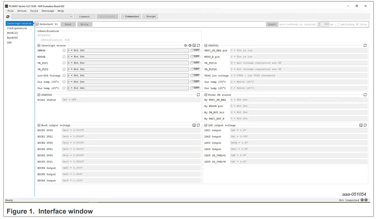
As shown in Figure 7, the PCA9451A software GUI is an user friendly tool to access the on-chip registers to perform write/read commands manually or automatically (depending on different setting chosen from the GUI). Below is a quick guide of the key blocks that the PCA9451A software GUI provides.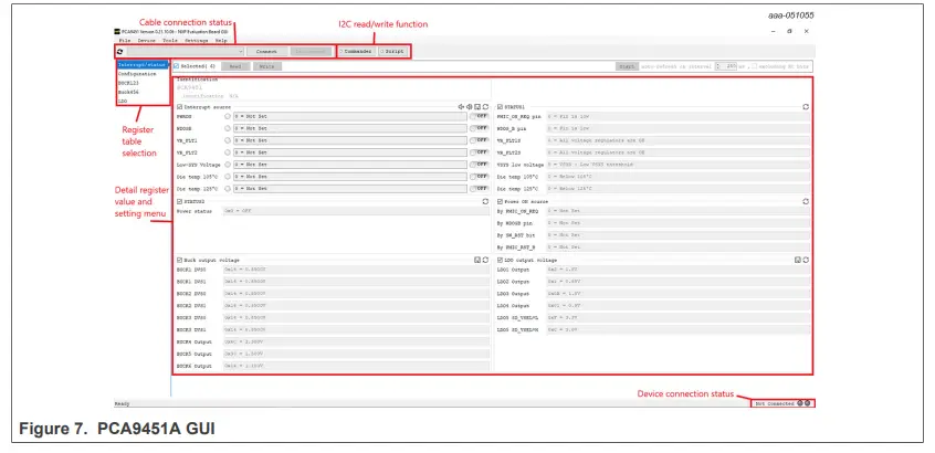 8.1 GUI setup
After turning on the power supply and plugging in the USB part of the FTDI cable, the GUI detects the cable automatically. Select the cable type (FT2TRWH9) from the drop-down menu, and then click “Connect” button. On the “Device connection status” section (right bottom part of the screen), the GUI shows “Connected” with green light.
8.2 Register table section
The registers are categorized as shown below:
- Interrupt/status – Includes status registers like Interrupts source, power status, power on source, and output regulator levels.
- Configuration – system configuration, power-up/power-down sequence control, reset behaviors, UVLO threshold, fault information, and level translator control.
- Buck123 – Includes all of the configuration registers for all Buck regulators 1, 2, and 3, including DVS controls.
- Buck456 – Includes all of the configuration registers for all Buck regulators 4, 5, and 6.
- LDO – Includes all of the configuration registers for all LDO regulators.
8.3 I C read and write
PCA9451A software GUI provides three ways to read and write.
- On register table, click the “read”/“write” button for the whole table, or click:
![]()
- Command. Read or write the Hex value to specific register.
- Script. Run the script to read or write a series of registers. Using guideline can be found in help menu.
PCA9451A evaluation steps
The following sections show how to perform evaluation of the PCA9451A using the evaluation board and the software GUI.
9.1 I C pullup configuration for proper GUI interface
This step must be done with the power supply turned off and USB cable disconnected. For I C interface
communication using the PCA9451A software GUI, remove J11 jumper (I2C_PU), and connect the red cable (3.3 V) from the FTDI cable to pin 1 of J3 connector (I C connector).
9.2 Jumper configuration
This step also needs to be done with the power supply turned off and USB cable disconnected. With exception of J11 jumper, please connect the jumpers in default configuration as shown in Section 6.3.
9.3 Connect and power the board
As shown in Figure 6, connect the wires of the FTDI cable and power supply according to the information in Section 7.2.1.
9.4 Working on the PCA9451A software GUI
Open, setup, and connect the GUI as directed in Section 8.1, then start configuring the PMIC using the different tabs.
9.4.1 BUCK configuration
Select ‘BUCKxxx’ tab from the register table selection.
From here you can change all the configuration registers for all the buck regulators of the PCA9451A, configure the low power modes, enable the active discharge resistor, use forced PWM, change enable modes, configure the DVS speed (for BUCK1, BUCK2 and BUCK3), and change output voltages by either by writing the value or using the horizontal slide bar.
Use the multimeter to check the voltage on the buck test points to confirm the voltage changes when configured.
9.4.2 LDO configuration
Select ‘LDO’ tab from the register table selection.
From here you can change all the configuration registers for all the LDO regulators of the PCA9451A, configure the low power modes, enable the active discharge resistor, change enable modes, and change output voltages by either by writing the value or using the horizontal slide bar.
Use the multimeter to check the voltage on the LDO test points to confirm the voltage changes when configured.
9.4.3 Load switch configuration
Select ‘LDO’ tab from the register table selection.
From here you can change all the configuration registers for the Load Switch of the PCA9451A, enable the active discharge resistor, change enable modes, and configure the different protection mechanisms.
9.4.4 GUI close
Click ‘Disconnect’ button, disconnect USB cable from the PC and turn OFF the Power Supply and close the PCA9451A GUI.
Schematic diagram
The schematic diagram of PCA9451A-EVK is available at URL: http://www.nxp.com/PCA9451A-EVK.
Bill of materials
The BOM of PCA9451A-EVK board is based on SCH-50786 REV A.
Table 8. PCA9451A-EVK BOM
| Description | Qty | BOM Ref | Manufacturers Name ~ Location | Manufacturers Part Number |
| CAP CER 10 μF 10V 10% X5R 0603 | 4 | C11, C14, C17, C20 | TDK | C1608X5R1A106K080AC |
| CAP CER 47 μF 10V 20% X5R 0805 | 2 | C28, C29 | TDK | C2012X5R1A476M125AC |
| CAP CER 4.7 μF 10V 10% X7S 0603 | 3 | C5, C22, C24 | MURATA | GRM188C71A475KE11D |
| CAP CER 22 μF 10V 20% X5R 0603 | 6 | C12, C15, C18, C21, C23, C25 | MURATA | GRM188R61A226ME15D |
| CAP CER 18pF 50V 5% C0G AEC- Q200 0402 | 2 | C3, C4 | MURATA | GCM1555C1H180JA16 |
| CAP CER 47 μF 6.3V 20% X5R 0603 | 3 | C13, C16, C19 | MURATA | GRM188R60J476ME15D |
| CAP CER 1 μF 10V 10% X7S 0402 | 7 | C1, C2, C6, C9, C10, C26, C27 | MURATA | GRM155C71A105KE11D |
| IND WW 0.47 μH@1MHz 3.4A 20% 2016 | 2 | L5, L6 | MURATA | 1286AS-H-R47M=P2 |
| IND PWR 0.47 μH@1MHZ 4.7A 20% SMT | 4 | L1, L2, L3, L4 | Shenzhen Sunlord Electronics Co., Ltd | WPN252012ER47MT |
| TEST POINT PC MULTI PURPOSE RED TH | 6 | TP7, TP8, TP9, TP10, TP11, TP12 | KEYSTONE ELECTRONICS | 5010 |
| TEST POINT ORANGE 70X220 MIL TH | 3 | TP1, TP4, TP5 | KEYSTONE ELECTRONICS | 5008 |
| TEST POINT WHITE 70X220 MIL TH | 1 | TP6 | KEYSTONE ELECTRONICS | 5007 |
| HDR 1X2 TH 100MIL SP 342H AU 118L | 9 | J6, J7, J11, J12, J13, J14, J33, J34, J36 | WURTH ELEKTRONIK EISOS GMBH & CO. KG (ELECTRONIC & ELECTROME HANICAL COMP) | 61300211121 |
| HDR 1X3 TH 2.54MM SP 344H AU 118L | 4 | J10, J20, J27, J29 | WURTH ELEKTRONIK EISOS GMBH & CO. KG (ELECTRONIC & ELECTROME HANICAL COMP) | 61300311121 |
| HDR 2X3 TH 100MIL CTR 344H AU 118L | 1 | J3 | WURTH ELEKTRONIK EISOS GMBH & CO. KG (ELECTRONIC & ELECTROME HANICAL COMP) | 61300621121 |
| HDR 2X8 TH 100MIL CTR 344H AU 118L | 2 | J4, J5 | WURTH ELEKTRONIK EISOS GMBH & CO. KG (ELECTRONIC & ELECTROME HANICAL COMP) | 61301621121 |
| CON 2 JUMPER PLUG SHORTING TH 200MIL SP 305H — | 5 | LK1, LK2, LK3, LK4, LK5 | KEYSTONE ELECTRONICS | 5026 |
| XTAL 32.768KHZ 12.5PF 20PPM 3.2 X1.5MM SMT | 1 | Y1 | ECS INC. INTERNATIONAL | ECS-.327-12.5-34B |
| Description | Qty | BOM Ref | Manufacturers Name ~ Location | Manufacturers Part Number |
| IC POWER MANAGEMENT 2.7-5.5V HVQFN56 | 1 | U1 | NXP SEMICONDUCTORS | PCA9451AHNY |
| RES MF ZERO OHM 1/16W 5% 0402 | 3 | R17, R18, R19 | SEI ELECTRONICS INC | RMCF1/16S0.005%R |
| RES MF 0.01 OHM 1/10W 1% AEC- Q200 0603 | 3 | R9, R10, R11 | Yageo | RL0603FR-070R01L |
| RES MF 100K 1/10W 5% AEC-Q200 0402 | 6 | R1, R4, R12, R13, R14, R15 | PANASONIC | ERJ2GEJ104X |
| RES MF 4.7K 1/10W 5% AEC-Q200 0402 | 8 | R2, R3, R5, R6, R7, R8, R20, R21 | PANASONIC | ERJ2GEJ472X |
| SW DIP 1 POS 0.025A@24VDC SMT | 2 | S1, S2 | WURTH ELEKTRONIK EISOS GMBH & CO. KG (ELECTRONIC & ELECTROME HANICAL COMP) | 416131160801 |
| SUBASSEMBLY HDR 1X3 TH 2.54MM SP 344H AU 118L + HDR 1X1 TH — 344H AU 118L | 1 | J30 | ||
| RES MF ZERO OHM — AEC-Q200 0603 | 0 | R16 | KOA SPEER | RK73Z1JTTD |
| DIODE SCH RECT 3A 40V AEC- Q101 SOD123W | 0 | D1, D2, D3, D4, D5, D6, D7, D8, D9, D10, D11, D12 | Experian | PMEG4030ER, 115 |
Legal information
12.1 Definitions
Draft — A draft status on a document indicates that the content is still under internal review and subject to formal approval, which may result in modifications or additions. NXP Semiconductors does not give any representations or warranties as to the accuracy or completeness of information included in a draft version of a document and shall have no liability for the consequences of use of such information.
12.2 Disclaimers
Limited warranty and liability — Information in this document is believed to be accurate and reliable. However, NXP Semiconductors does not give any representations or warranties, expressed or implied, as to the accuracy or completeness of such information and shall have no liability for the consequences of use of such information. NXP Semiconductors takes no responsibility for the content in this document if provided by an information source outside of NXP Semiconductors.
In no event shall NXP Semiconductors be liable for any indirect, incidental, punitive, special or consequential damages (including – without limitation lost profits, lost savings, business interruption, costs related to the removal or replacement of any products or rework charges) whether or not such damages are based on tort (including negligence), warranty, breach of contract or any other legal theory.
Notwithstanding any damages that customer might incur for any reason whatsoever, NXP Semiconductors’ aggregate and cumulative liability towards customer for the products described herein shall be limited in accordance with the Terms and conditions of commercial sale of NXP Semiconductors.
Right to make changes — NXP Semiconductors reserves the right to make changes to information published in this document, including without limitation specifications and product descriptions, at any time and without notice. This document supersedes and replaces all information supplied prior to the publication hereof.
Suitability for use — NXP Semiconductors products are not designed, authorized or warranted to be suitable for use in life support, life-critical or safety-critical systems or equipment, nor in applications where failure or malfunction of an NXP Semiconductors product can reasonably be expected to result in personal injury, death or severe property or environmental damage. NXP Semiconductors and its suppliers accept no liability for inclusion and/or use of NXP Semiconductors products in such equipment or applications and therefore such inclusion and/or use is at the customer’s own risk.
Applications — Applications that are described herein for any of these products are for illustrative purposes only. NXP Semiconductors makes no representation or warranty that such applications will be suitable for the specified use without further testing or modification. Customers are responsible for the design and operation of their applications and products using NXP Semiconductors products, and NXP
Semiconductors accepts no liability for any assistance with applications or customer product design. It is customer’s sole responsibility to determine whether the NXP Semiconductors product is suitable and fit for the customer’s applications and products planned, as well as for the planned application and use of customer’s third party customer(s). Customers should provide appropriate design and operating safeguards to minimize the risks associated with their applications and products. NXP Semiconductors does not accept any liability related to any default, damage, costs or problem which is based on any weakness or default in the customer’s applications or products, or the application or use by customer’s third party customer(s). Customer is responsible for doing all necessary testing for the customer’s applications and products using NXP Semiconductors products in order to avoid a default of the applications and the products or of the application or use by customer’s third party customer(s). NXP does not accept any liability in this respect.
Terms and conditions of commercial sale — NXP Semiconductors products are sold subject to the general terms and conditions of commercial sale, as published at http://www.nxp.com/profile/terms, unless otherwise agreed in a valid written individual agreement. In case an individual agreement is concluded only the terms and conditions of the respective agreement shall apply. NXP Semiconductors hereby expressly objects to applying the customer’s general terms and conditions with regard to the
purchase of NXP Semiconductors products by customer.
Export control — This document as well as the item(s) described herein may be subject to export control regulations. Export might require a prior authorization from competent authorities.
Suitability for use in non-automotive qualified products — Unless this data sheet expressly states that this specific NXP Semiconductors product is automotive qualified, the product is not suitable for automotive use. It is neither qualified nor tested in accordance with automotive testing or application requirements. NXP Semiconductors accepts no liability for inclusion and/or use of non-automotive qualified products in automotive equipment or applications.
In the event that customer uses the product for design-in and use in automotive applications to automotive specifications and standards, customer (a) shall use the product without NXP Semiconductors’ warranty of the product for such automotive applications, use and specifications, and (b) whenever customer uses the product for automotive applications beyond NXP Semiconductors’ specifications such use shall be solely at customer’s own risk, and (c) customer fully indemnifies NXP Semiconductors for any liability, damages or failed product claims resulting from customer design and use of the product for automotive applications beyond NXP Semiconductors’ standard warranty and NXP Semiconductors’ product specifications.
Translations — A non-English (translated) version of a document, including the legal information in that document, is for reference only. The English version shall prevail in case of any discrepancy between the translated and English versions.
Security — Customer understands that all NXP products may be subject to unidentified vulnerabilities or may support established security standards or specifications with known limitations. Customer is responsible for the design and operation of its applications and products throughout their lifecycles to reduce the effect of these vulnerabilities on customer’s applications and products. Customer’s responsibility also extends to other open and/or proprietary technologies supported by NXP products for use in customer’s applications. NXP accepts no liability for any vulnerability. Customer should regularly check security updates from NXP and follow up appropriately.
Customer shall select products with security features that best meet rules, regulations, and standards of the intended application and make the ultimate design decisions regarding its products and is solely responsible for compliance with all legal, regulatory, and security related requirements concerning its products, regardless of any information or support that may be provided by NXP. NXP has a Product Security Incident Response Team (PSIRT) (reachable at [email protected]) that manages the investigation, reporting, and solution release to security vulnerabilities of NXP products.
12.3 Trademarks
Notice: All referenced brands, product names, service names, and trademarks are the property of their respective owners.
NXP — wordmark and logo are trademarks of NXP B.V.
Please be aware that important notices concerning this document and the product(s) described herein, have been included in section ‘Legal information’.
© 2023 NXP B.V.
For more information, please visit: http://www.nxp.com
All rights reserved.
Date of release: 30 March 2023
Document identifier: UM11883


