 IRFP250
Vishay Siliconix
Power MOSFET
TO-247AC
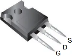
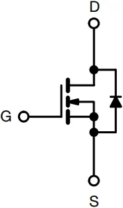
N-Channel MOSFET
| PRODUCT SUMMARY | ||
VDS (V) | 200 | |
| RDS(on) (Ω) | VGS = 10 V | 0.085 |
Qg (max.) (nC) | 140 | |
| Qgs (nC) | 28 | |
Qgd (nC) | 74 | |
| Configuration | Single | |
FEATURES

- Dynamic dV/dt rating
- Repetitive avalanche rated
- Isolated central mounting hole
- Fast switching
- Ease of Paralleling
- Simple drive requirements
- Material categorization: for definitions of compliance please see www.vishay.com/doc?99912
Note
* This datasheet provides information about parts that are RoHS-compliant and / or parts that are non RoHS-compliant. For example, parts with lead (Pb) terminations are not RoHS-compliant. Please see the information / tables in this datasheet for details
DESCRIPTION
Third generation Power MOSFETs from Vishay provide the designer with the best combination of fast switching, ruggedized device design, low on-resistance and cost-effectiveness.
The TO-220AB package is universially preferred for commercial-industrial applications where higher power levels preclude the use of TO-220AB devices. The TO-247AC is similar but superior to the earlier TO-218 package because of its isolated mounting hole. It also provides greater creepage distance between pins to meet the requirements of most safety specifications.
| ORDERING INFORMATION | |
| Package | TO-247AC |
| Lead (Pb)-free | IRFP250PbF |
| ABSOLUTE MAXIMUM RATINGS (TC = 25 °C, unless otherwise noted) | |||||
| PARAMETER | SYMBOL | LIMIT | UNIT | ||
| Drain-source voltage | VDS | 200 | V | ||
| Gate-source voltage | VGS | ± 20 | |||
| Continuous drain current | VGS at 10 V | TC = 25 °C | ID | 30 | A |
| TC = 100 °C | 19 | ||||
| Pulsed drain current a | IDM | 120 | |||
| Linear derating factor | 1.5 | W/°C | |||
| Single pulse avalanche energy b | EAS | 410 | mJ | ||
| Repetitive avalanche current a | IAR | 30 | A | ||
| Repetitive avalanche energy a | EAR | 19 | mJ | ||
| Maximum power dissipation | TC = 25 °C | PD | 190 | W | |
| Peak diode recovery dV/dt c | dV/dt | 5.0 | V/ns | ||
| Operating junction and storage temperature range | TJ, Tstg | -55 to +150 | °C | ||
| Soldering recommendations (peak temperature) d | for 10 s | 300 | |||
| Mounting torque | 6-32 or M3 screw | 10 | lbf · in | ||
1.1 | N · m | ||||
Notes
a. Repetitive rating; pulse width limited by maximum junction temperature (see fig. 11)
b. VDD = 50 V, starting TJ = 25 °C, L = 683 μH, Rg = 25 Ω, IAS = 30 A (see fig. 12)
c. ISD ≤ 30 A, dI/dt ≤ 190 A/μs, VDD ≤ VDS, TJ ≤ 150 °C
d. 1.6 mm from case
| THERMAL RESISTANCE RATINGS | ||||
| PARAMETER | SYMBOL | TYP. | MAX. | UNIT |
| Maximum junction-to-ambient | RthJA | – | 40 | °C/W |
| Case-to-sink, flat, greased surface | RthCS | 0.24 | – | |
| Maximum junction-to-case (drain) | RthJC | – | 0.65 | |
| SPECIFICATIONS (TJ = 25 °C, unless otherwise noted) | |||||||
| PARAMETER | SYMBOL | TEST CONDITIONS | MIN. | TYP. | MAX. | UNIT | |
| Static | |||||||
| Drain-source breakdown voltage | VDS | VGS = 0 V, ID = 250 μA | 200 | – | – | V | |
| VDS temperature coefficient | ΔVDS/TJ | Reference to 25 °C, ID = 1 mA | – | 0.27 | – | V/°C | |
| Gate-source threshold voltage | VGS(th) | VDS = VGS, ID = 250 μA | 2.0 | – | 4.0 | V | |
| Gate-source leakage | IGSS | VGS = ± 20 V | – | – | ± 100 | nA | |
| Zero gate voltage drain current | IDSS | VDS = 200 V, VGS = 0 V | – | – | 25 | μA | |
| VDS = 160 V, VGS = 0 V, TJ = 125 °C | – | – | 250 | ||||
| Drain-source on-state resistance | RDS(on) | VGS = 10 V | ID = 18 A b | – | – | 0.085 | Ω |
| Forward transconductance | gfs | VDS = 50 V, ID = 18 A | 12 | – | – | S | |
| Dynamic | |||||||
| Input capacitance | Ciss | VGS = 0 V, VDS = 25 V, f = 1.0 MHz, see fig. 5 | – | 2800 | – | pF | |
| Output capacitance | Coss | – | 780 | – | |||
| Reverse transfer capacitance | Crss | – | 250 | – | |||
| Total gate charge | Qg | VGS = 10 V | ID = 30 A, VDS = 160 V, see fig. 6 and 13 b | – | – | 140 | nC |
| Gate-source charge | Qgs | – | – | 28 | |||
| Gate-drain charge | Qgd | – | – | 74 | |||
| Turn-on delay time | td(on) | VDD = 100 V, ID = 30 A, Rg = 6.2 Ω, RD = 3.2 Ω, see fig. 10 b | – | 16 | – | ns | |
| Rise time | tr | – | 86 | – | |||
| Turn-off delay time | td(off) | – | 70 | – | |||
| Fall time | tf | – | 62 | – | |||
| Internal drain inductance | LD | 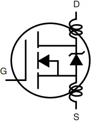 Between lead, 6 mm (0.25″) from package and center of die contact | – | 5.0 | – | nH | |
| Internal source inductance | LS | – | 13 | – | |||
| Drain-Source Body Diode Characteristics | |||||||
| Continuous source-drain diode current | IS | 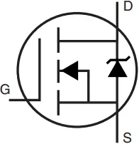 MOSFET symbol showing the integral reverse p – n junction diode MOSFET symbol showing the integral reverse p – n junction diode | – | – | 30 | A | |
| Pulsed diode forward current a | ISM | – | – | 120 | |||
| Body diode voltage | VSD | TJ = 25 °C, IS = 30 A, VGS = 0 V b | – | – | 2.0 | V | |
| Body diode reverse recovery time | trr | TJ = 25 °C, IF = 30 A, dI/dt = 100 A/ms | – | 360 | 540 | ns | |
| Body diode reverse recovery charge | Qrr | – | 4.6 | 6.9 | μC | ||
| Forward turn-on time | ton | Intrinsic turn-on time is negligible (turn-on is dominated by LS and LD) | |||||
Notes
a. Repetitive rating; pulse width limited by maximum junction temperature (see fig. 11)
b. Pulse width ≤ 300 μs; duty cycle ≤ 2 %
TYPICAL CHARACTERISTICS (25 °C, unless otherwise noted)
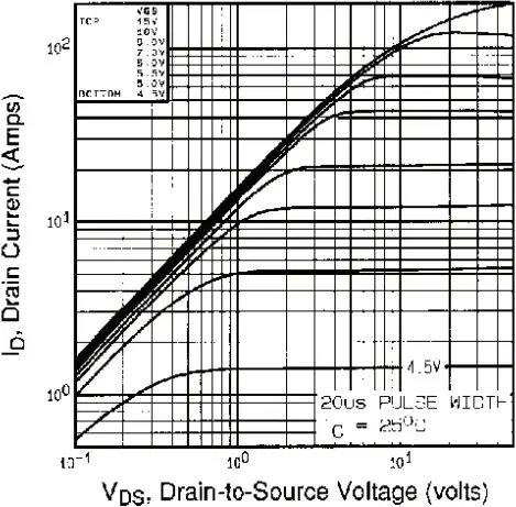
Fig. 1 – Typical Output Characteristics, TC = 25 °C
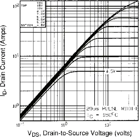 Fig. 2 – Typical Output Characteristics, TC = 150 °C
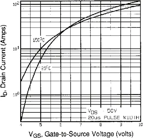
Fig. 3 – Typical Transfer Characteristics
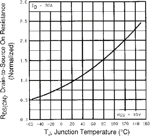
Fig. 4 – Normalized On-Resistance vs. Temperature
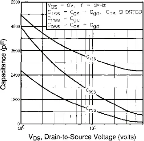
Fig. 5 – Typical Capacitance vs. Drain-to-Source Voltage
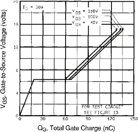
Fig. 6 – Typical Gate Charge vs. Gate-to-Source Voltage
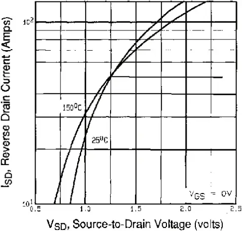
Fig. 7 – Typical Source-Drain Diode Forward Voltage
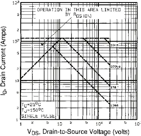
Fig. 8 – Maximum Safe Operating Area
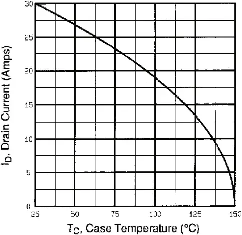
Fig. 9 – Maximum Drain Current vs. Case Temperature
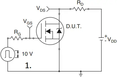
Fig. 10a – Switching Time Test Circuit
- Pulse width ≤ 1 µs
Duty factor ≤ 0.1 %
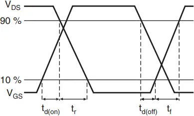
Fig. 10b – Switching Time Waveforms
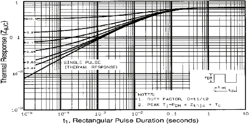
Fig. 11 – Maximum Effective Transient Thermal Impedance, Junction-to-Case
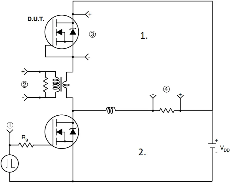
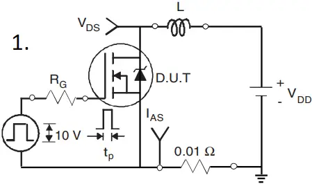 Fig. 12a – Unclamped Inductive Test Circuit
- Vary tp to obtain required IAS
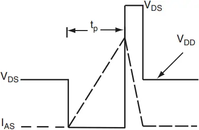
Fig. 12b – Unclamped Inductive Waveforms
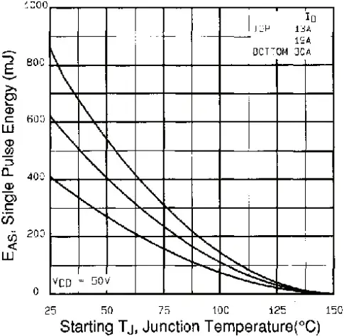
Fig. 12c – Maximum Avalanche Energy vs. Drain Current
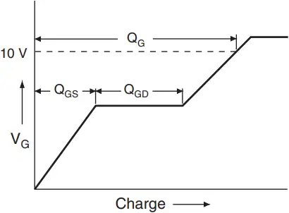
Fig. 13a – Basic Gate Charge Waveform
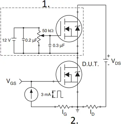
Fig. 13b – Gate Charge Test
- Current regulator
Same type as D.U.T. - Current sampling resistors
Peak Diode Recovery dV/dt Test Circuit
- Circuit layout considerations
• Low stray inductance
• Ground plane
• Low leakage inductance current transformer - • dV/dt controlled by Rg
• Driver same type as D.U.T.
• ISD controlled by duty factor “D”
• D.U.T. – device under test
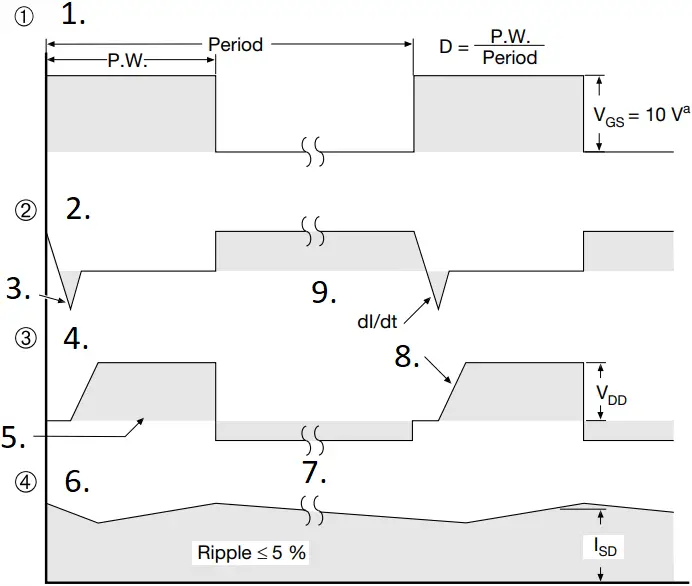
Fig. 14 – For N-Channel
Note
a. VGS = 5 V for logic level devices
- Driver gate drive
- D.U.T. lSD waveform
- Reverse recovery current
- D.U.T. VDS waveform
- Re-applied voltage
- Inductor current
- Body diode forward drop
- Diode recovery
dV/dt - Body diode forward current
Vishay Siliconix maintains worldwide manufacturing capability. Products may be manufactured at one of several qualified locations. Reliability data for Silicon Technology and Package Reliability represent a composite of all qualified locations. For related documents such as package/tape drawings, part marking, and reliability data, see www.vishay.com/ppg?91212.
S22-0046, Rev. C, 24-Jan-2021 Document Number: 91212
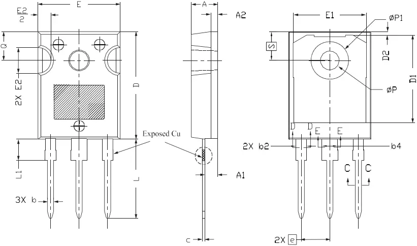
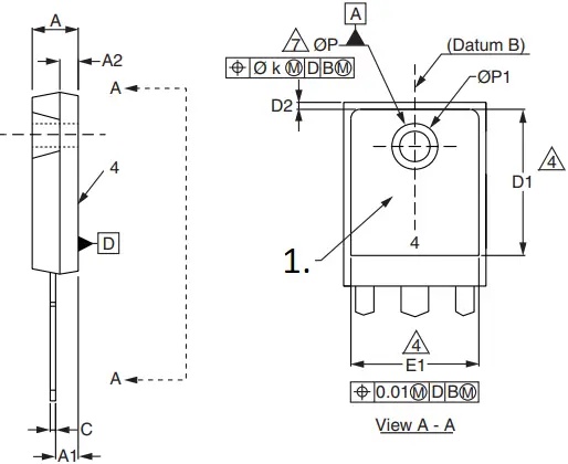
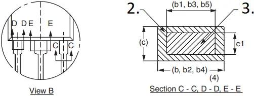
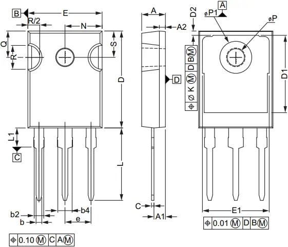
Package Information
TO-247AC (High Voltage)
VERSION 1: FACILITY CODE = 9
![]()
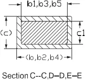
| MILLIMETERS | ||||
| DIM. | MIN. | NOM. | MAX. | NOTES |
A | 4.83 | 5.02 | 5.21 | |
| A1 | 2.29 | 2.41 | 2.55 | |
A2 | 1.17 | 1.27 | 1.37 | |
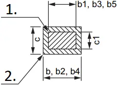
| b | 1.12 | 1.20 | 1.33 | |
b1 | 1.12 | 1.20 | 1.28 | |
| b2 | 1.91 | 2.00 | 2.39 | 6 |
b3 | 1.91 | 2.00 | 2.34 | |
| b4 | 2.87 | 3.00 | 3.22 | 6, 8 |
b5 | 2.87 | 3.00 | 3.18 | |
| c | 0.40 | 0.50 | 0.60 | 6 |
c1 | 0.40 | 0.50 | 0.56 | |
| D | 20.40 | 20.55 | 20.70 | 4 |
D1 | 16.46 | 16.76 | 17.06 | 5 |
| D2 | 0.56 | 0.66 | 0.76 | |
E | 15.50 | 15.70 | 15.87 | 4 |
| E1 | 13.46 | 14.02 | 14.16 | 5 |
E2 | 4.52 | 4.91 | 5.49 | 3 |
| e | 5.46 BSC | |||
L | 14.90 | 15.15 | 15.40 | |
| L1 | 3.96 | 4.06 | 4.16 | 6 |
Ø P | 3.56 | 3.61 | 3.65 | 7 |
| Ø P1 | 7.19 ref. | |||
Q | 5.31 | 5.50 | 5.69 | |
| S | 5.51 BSC | |||
Notes
(1) Package reference: JEDEC® TO247, variation AC
(2) All dimensions are in mm
(3) Slot required, notch may be rounded
(4) Dimension D and E do not include mold flash. Mold flash shall not exceed 0.127 mm per side. These dimensions are measured at the outermost extremes of the plastic body
(5) Thermal pad contour optional with dimensions D1 and E1
(6) Lead finish uncontrolled in L1
(7) Ø P to have a maximum draft angle of 1.5° to the top of the part with a maximum hole diameter of 3.91 mm
(8) Dimension b2 and b4 does not include dambar protrusion. Allowable dambar protrusion shall be 0.1 mm total in excess of b2 and b4 dimension at maximum material condition
VERSION 2: FACILITY CODE = Y
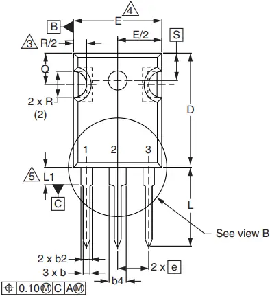
Lead Assignments
- Gate
- Drain
- Source
- Drain
- Thermal pad
- Planting
- Base metal
MILLIMETERS | |||
| DIM. | MIN. | MAX. | NOTES |
A | 4.58 | 5.31 | |
| A1 | 2.21 | 2.59 | |
A2 | 1.17 | 2.49 | |
| b | 0.99 | 1.40 | |
b1 | 0.99 | 1.35 | |
| b2 | 1.53 | 2.39 | |
b3 | 1.65 | 2.37 | |
| b4 | 2.42 | 3.43 | |
b5 | 2.59 | 3.38 | |
| c | 0.38 | 0.86 | |
c1 | 0.38 | 0.76 | |
| D | 19.71 | 20.82 | |
D1 | 13.08 | – | |
D2 | 0.51 | 1.30 | |
| E | 15.29 | 15.87 | |
E1 | 13.72 | – | |
| e | 5.46 BSC | ||
Ø k | 0.254 | ||
| L | 14.20 | 16.25 | |
L1 | 3.71 | 4.29 | |
| Ø P | 3.51 | 3.66 | |
Ø P1 | – | 7.39 | |
| Q | 5.31 | 5.69 | |
R | 4.52 | 5.49 | |
| S | 5.51 BSC | ||
Notes
(1) Dimensioning and tolerancing per ASME Y14.5M-1994
(2) Contour of slot optional
(3) Dimension D and E do not include mold flash. Mold flash shall not exceed 0.127 mm (0.005″) per side. These dimensions are measured at the outermost extremes of the plastic body
(4) Thermal pad contour optional with dimensions D1 and E1
(5) Lead finish uncontrolled in L1
(6) Ø P to have a maximum draft angle of 1.5 to the top of the part with a maximum hole diameter of 3.91 mm (0.154″)
(7) Outline conforms to JEDEC outline TO-247 with exception of dimension c
VERSION 3: FACILITY CODE = N
![]()
- Base metal
- Plating
MILLIMETERS | ||
| DIM. | MIN. | MAX. |
A | 4.65 | 5.31 |
| A1 | 2.21 | 2.59 |
A2 | 1.17 | 1.37 |
| b | 0.99 | 1.40 |
b1 | 0.99 | 1.35 |
| b2 | 1.65 | 2.39 |
b3 | 1.65 | 2.34 |
| b4 | 2.59 | 3.43 |
b5 | 2.59 | 3.38 |
| c | 0.38 | 0.89 |
c1 | 0.38 | 0.84 |
| D | 19.71 | 20.70 |
D1 | 13.08 | – |
| D2 | 0.51 | 1.35 |
E | 15.29 | 15.87 |
| E1 | 13.46 | – |
e | 5.46 BSC | |
| k | 0.254 | |
L | 14.20 | 16.10 |
| L1 | 3.71 | 4.29 |
N | 7.62 BSC | |
| P | 3.56 | 3.66 |
P1 | – | 7.39 |
| Q | 5.31 | 5.69 |
R | 4.52 | 5.49 |
| S | 5.51 BSC | |
| ECN: E22-0452-Rev. G, 31-Oct-2022 DWG: 5971 | ||
Notes
(1) Dimensioning and tolerancing per ASME Y14.5M-1994
(2) Contour of slot optional
(3) Dimension D and E do not include mold flash. Mold flash shall not exceed 0.127 mm (0.005″) per side. These dimensions are measured at the outermost extremes of the plastic body
(4) Thermal pad contour optional with dimensions D1 and E1
(5) Lead finish uncontrolled in L1
(6) Ø P to have a maximum draft angle of 1.5 to the top of the part with a maximum hole diameter of 3.91 mm (0.154″)
Revision: 31-Oct-2022 Document Number: 91360
For technical questions, contact: [email protected]
THIS DOCUMENT IS SUBJECT TO CHANGE WITHOUT NOTICE. THE PRODUCTS DESCRIBED HEREIN AND THIS DOCUMENT ARE SUBJECT TO SPECIFIC DISCLAIMERS, SET FORTH AT www.vishay.com/doc?91000
Legal Disclaimer Notice
Disclaimer
ALL PRODUCT, PRODUCT SPECIFICATIONS AND DATA ARE SUBJECT TO CHANGE WITHOUT NOTICE TO IMPROVE RELIABILITY, FUNCTION OR DESIGN OR OTHERWISE.
Vishay Intertechnology, Inc., its affiliates, agents, and employees, and all persons acting on its or their behalf (collectively, “Vishay”), disclaim any and all liability for any errors, inaccuracies or incompleteness contained in any datasheet or in any other disclosure relating to any product.
Vishay makes no warranty, representation or guarantee regarding the suitability of the products for any particular purpose or the continuing production of any product. To the maximum extent permitted by applicable law, Vishay disclaims (i) any and all liability arising out of the application or use of any product, (ii) any and all liability, including without limitation special, consequential or incidental damages, and (iii) any and all implied warranties, including warranties of fitness for particular purpose, non-infringement and merchantability.
Statements regarding the suitability of products for certain types of applications are based on Vishay’s knowledge of typical requirements that are often placed on Vishay products in generic applications. Such statements are not binding statements about the suitability of products for a particular application. It is the customer’s responsibility to validate that a particular product with the properties described in the product specification is suitable for use in a particular application. Parameters provided in datasheets and / or specifications may vary in different applications and performance may vary over time. All operating parameters, including typical parameters, must be validated for each customer application by the customer’s technical experts. Product specifications do not expand or otherwise modify Vishay’s terms and conditions of purchase, including but not limited to the warranty expressed therein.
Hyperlinks included in this datasheet may direct users to third-party websites. These links are provided as a convenience and for informational purposes only. Inclusion of these hyperlinks does not constitute an endorsement or an approval by Vishay of any of the products, services or opinions of the corporation, organization or individual associated with the third-party website. Vishay disclaims any and all liability and bears no responsibility for the accuracy, legality or content of the third-party website or for that of subsequent links.
Except as expressly indicated in writing, Vishay products are not designed for use in medical, life-saving, or life-sustaining applications or for any other application in which the failure of the Vishay product could result in personal injury or death. Customers using or selling Vishay products not expressly indicated for use in such applications do so at their own risk. Please contact authorized Vishay personnel to obtain written terms and conditions regarding products designed for such applications.
No license, express or implied, by estoppel or otherwise, to any intellectual property rights is granted by this document or by any conduct of Vishay. Product names and markings noted herein may be trademarks of their respective owners.
© 2023 VISHAY INTERTECHNOLOGY, INC. ALL RIGHTS RESERVED
Revision: 01-Jan-2023 Document Number: 91000
Downloaded from Arrow.com.


