VISHAY IRF9610 Siliconix Instructions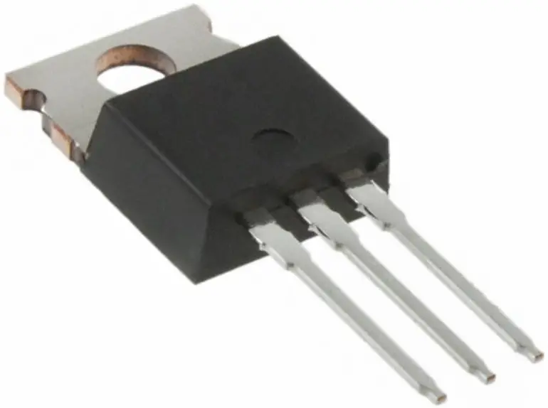
PRODUCT SUMMARY
| VDS (V) | -200 | |
| RDS(on) (L) | VGS = -10 V | 3.0 |
| Qg max. (nC) | 11 | |
| Qgs (nC) | 7.0 | |
| Qgd (nC) | 4.0 | |
| Configuration | Single | |
FEATURES
- Dynamic dV/dt rating
- P-channel
- Fast switching
- Ease of paralleling
- Simple drive requirements
- Material categorization: for definitions of compliance please see www.vishay.com/doc?99912
Note
- This datasheet provides information about parts that are RoHS-compliant and / or parts that are non RoHS-compliant. For example, parts with lead (Pb) terminations are not RoHS-compliant. Please see the information / tables in this datasheet for details.
DESCRIPTION
The power MOSFETs technology is the key to Vishay’s advanced line of Power MOSFET transistors. The efficient geometry and unique processing of the Power MOSFETs design achieve very low on-state resistance combined with high transconductance and extreme device ruggedness. The TO-220AB package is universally preferred for all commercial-industrial applications at power dissipation levels to approximately 50 W. The low thermal resistance and low package cost of the TO-220AB contribute to its wide acceptance throughout the industry.
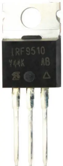
ORDERING INFORMATION
| Package | TO-220AB |
| Lead (Pb)-free | IRF9610PbF |
| Lead (Pb)-free and halogen-free | IRF9610PbF-BE3 |
ABSOLUTE MAXIMUM RATINGS
(S (TC = 25 °C, unless otherwise noted)
| PARAMETER | SYMBOL | LIMIT | UNIT | ||
| Drain-source voltage | VDS | -200 | V | ||
| Gate-source voltage | VGS | ± 20 | |||
| Continuous drain current | VGS at 10 V | TC = 25 °C | ID | -1.8 | A |
| TC = 100 °C | -1.0 | ||||
| Pulsed drain current a | IDM | -7.0 | |||
| Linear derating factor | 0.16 | W/°C | |||
| Single pulse avalanche energy b | PD | 20 | W | ||
| Repetitive avalanche current a | ILM | -7.0 | A | ||
| Repetitive avalanche energy a | dV/dt | -5.0 | V/ns | ||
| Maximum power dissipation | TC = 25 °C | TJ, Tstg | -55 to +150 | °C | |
| Peak diode recovery dV/dt c | 300 | ||||
| Operating junction and storage temperature range | 10 | lbf · in | |||
| Soldering recommendations (peak temperature) d | For 10 s | 1.1 | N · m | ||
Notes
- Repetitive rating; pulse width limited by maximum junction temperature (see fig. 5)
- Not applicable
- ISD ≤ -1.8 A, dI/dt ≤ 70 A/μs, VDD ≤ VDS, TJ ≤ 150 °C
- 1.6 mm from cas
THERMAL RESISTANCE RATINGS
| PARAMETER | SYMBOL | TYP. | MAX. | UNIT |
| Maximum junction-to-ambient | RthJA | – | 62 | °C/W |
| Case-to-sink, flat, greased surface | RthCS | 0.50 | – | |
| Maximum junction-to-case (drain) | RthJC | – | 6.4 |
SPECIFICATIONS
(TJ = 25 °C, unless otherwise noted)
| PARAMETER | SYMBOL | TEST CONDITIONS | MIN. | TYP. | MAX. | UNIT | |
| Static | |||||||
| Drain-source breakdown voltage | VDS | VGS = 0 V, ID = -250 μA | -200 | – | – | V | |
| VDS temperature coefficient | DVDS/TJ | Reference to 25 °C, ID = -1 mA | – | -0.23 | – | V/°C | |
| Gate-source threshold voltage | VGS(th) | VDS = VGS, ID = -250 μA | -2.0 | – | -4.0 | V | |
| Gate-source leakage | IGSS | VGS = ± 20 V | – | – | ± 100 | nA | |
| Zero gate voltage drain current | IDSS | VDS = -200 V, VGS = 0 V | – | – | -100 | μA | |
| VDS = -160 V, VGS = 0 V, TJ = 125 °C | – | – | -500 | ||||
| Drain-source on-state resistance | RDS(on) | VGS = -10 V | ID = -0.90 A b | – | – | 3.0 | L |
| Forward transconductance | gfs | VDS = -50 V, ID = -0.90 A b | 0.90 | – | – | S | |
| Dynamic | |||||||
| Input capacitance | Ciss | VGS = 0 V, VDS = -25 V,f = 1.0 MHz, see fig. 10 | – | 170 | – | pF | |
| Output capacitance | Coss | – | 50 | – | |||
| Reverse transfer capacitance | Crss | – | 15 | – | |||
| Total gate charge | Qg | VGS = -10 V | ID = -3.5 A, VDS = -160 V, see fig. 11 and 18 b | – | – | 11 | nC |
| Gate-source charge | Qgs | – | – | 7.0 | |||
| Gate-drain charge | Qgd | – | – | 4.0 | |||
| Turn-on delay time | td(on) | VDD = -100 V, ID = -0.90 A,Rg = 50 L, RD = 110 L, see fig. 17 b | – | 8.0 | – |
ns | |
| Rise time | tr | – | 15 | – | |||
| Turn-off delay time | td(off) | – | 10 | – | |||
| Fall time | tf | – | 8.0 | – | |||
| Gate input resistance | Rg | f = 1 MHz, open drain | 2.5 | – | 14.3 | L | |
| Internal drain inductance | LD | Between lead, D6 mm (0.25″) from package and center of Guidie contactS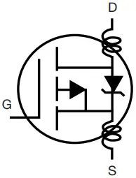 | – | 4.5 | – | nH | |
| Internal source inductance | LS | – | 7.5 | – | |||
| Drain-Source Body Diode Characteristics | |||||||
| Continuous source-drain diode current | IS | MOSFET symbol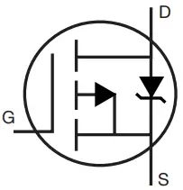 Showing the integral reverse Gp – n junction diodeS | – | – | -1.8 | A | |
| Pulsed diode forward current a | ISM | – | – | -7.0 | |||
| Body diode voltage | VSD | TJ = 25 °C, IS = -1.8 A, VGS = 0 V b | – | – | -5.8 | V | |
| Body diode reverse recovery time | trr | TJ = 25 °C, IF = -1.8 A, dI/dt = 100 A/μs b | – | 240 | 360 | ns | |
| Body diode reverse recovery charge | Qrr | – | 1.7 | 2.6 | μC | ||
| Forward turn-on time | ton | Intrinsic turn-on time is negligible (turn-on is dominated by LS and LD) | |||||
Notes
- Repetitive rating; pulse width limited by maximum junction temperature (see fig. 5)
- Pulse width ≤ 300 μs; duty cycle ≤ 2 %
TYPICAL CHARACTERISTICS
(25 °C, unless otherwise noted)
Fig. 1 – Typical Output Characteristics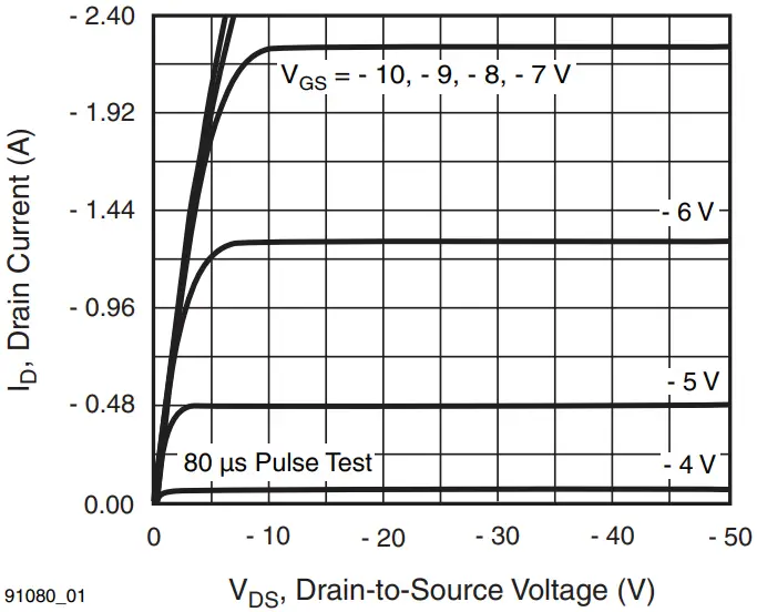
Fig. 2 – Typical Transfer Characteristics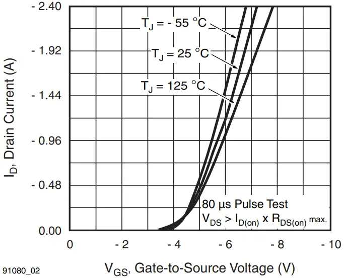
Fig. 3 – Typical Saturation Characteristics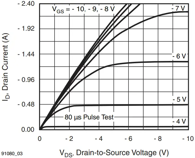
Fig. 4 – Maximum Safe Operating Area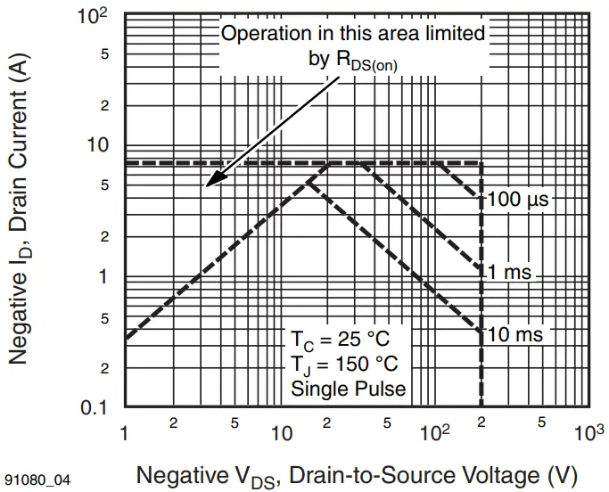
Fig. 5 – Maximum Effective Transient Thermal Impedance, Junction-to-Case vs. Pulse Duration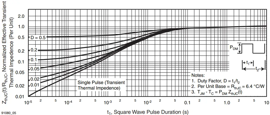
Fig. 6 – Typical Transconductance vs. Drain Current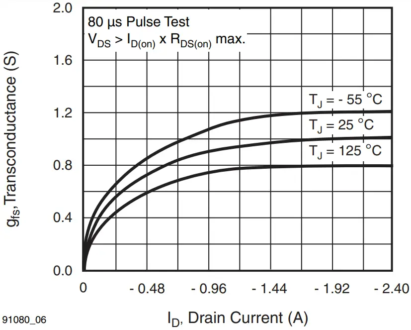
Fig. 7 – Typical Source-Drain Diode Forward Voltage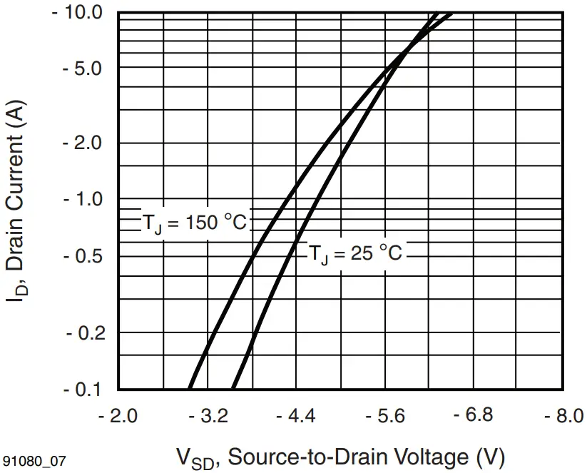
Fig. 8 – Breakdown Voltage vs. Temperature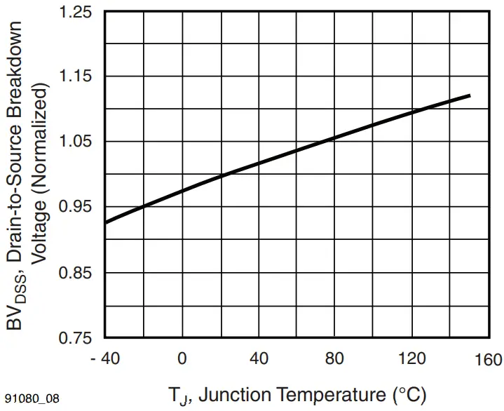
Fig. 9 – Normalized On-Resistance vs. Temperature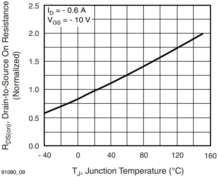
Fig. 10 – Typical Capacitance vs. Drain-to-Source Voltage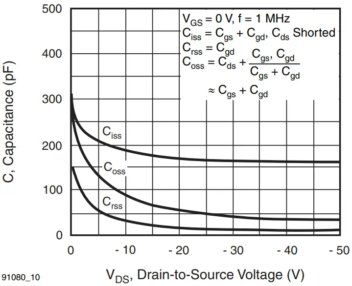
Fig. 11 – Typical Gate Charge vs. Gate-to-Source Voltage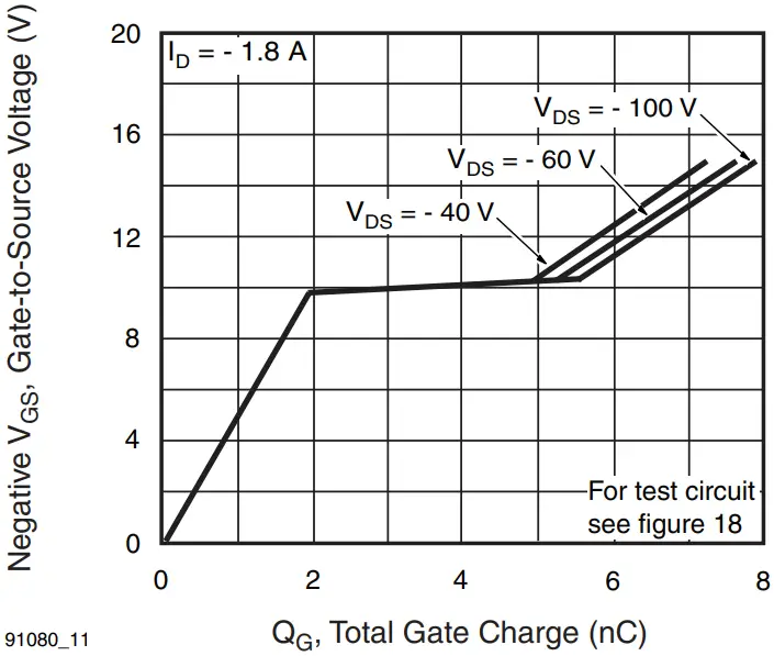
Fig. 12 – Typical On-Resistance vs. Drain Current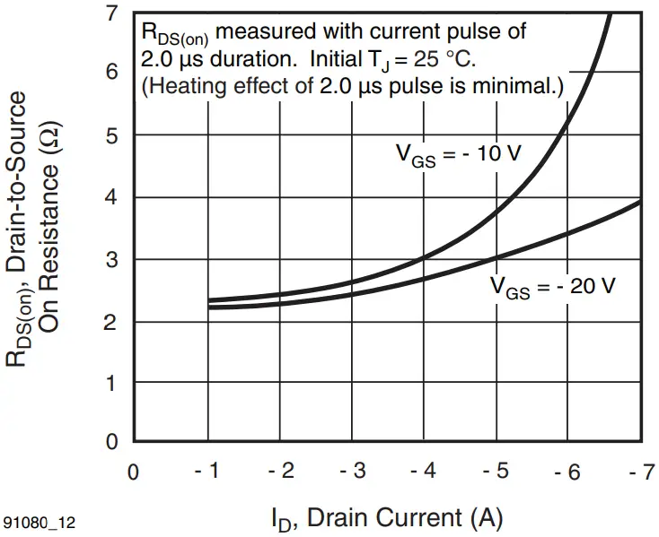
Fig. 13 – Maximum Drain Current vs. Case Temperature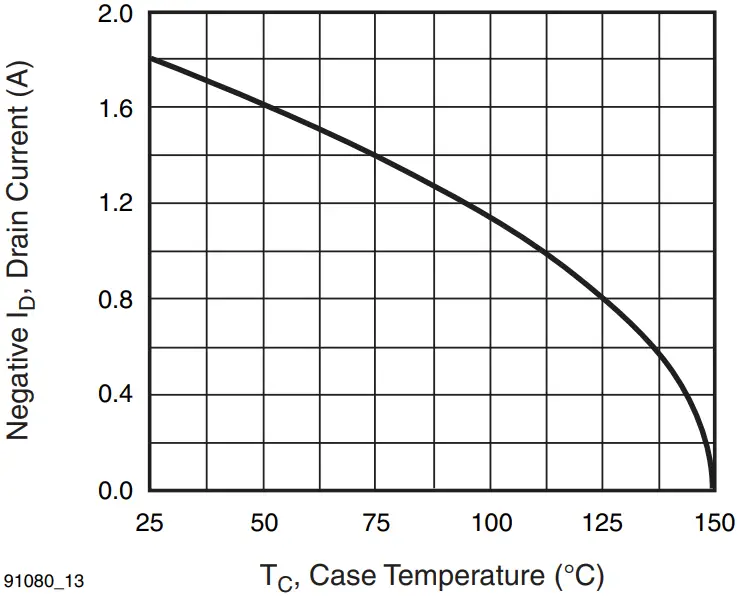
Fig. 14 – Power vs. Temperature Derating Curve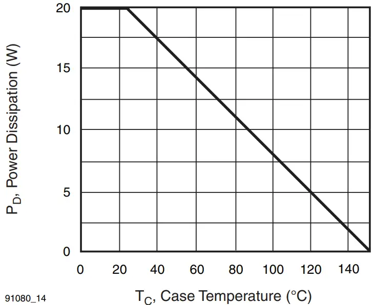
Fig. 15 – Clamped Inductive Test Circuit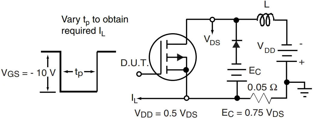
Fig. 16 – Clamped Inductive Waveforms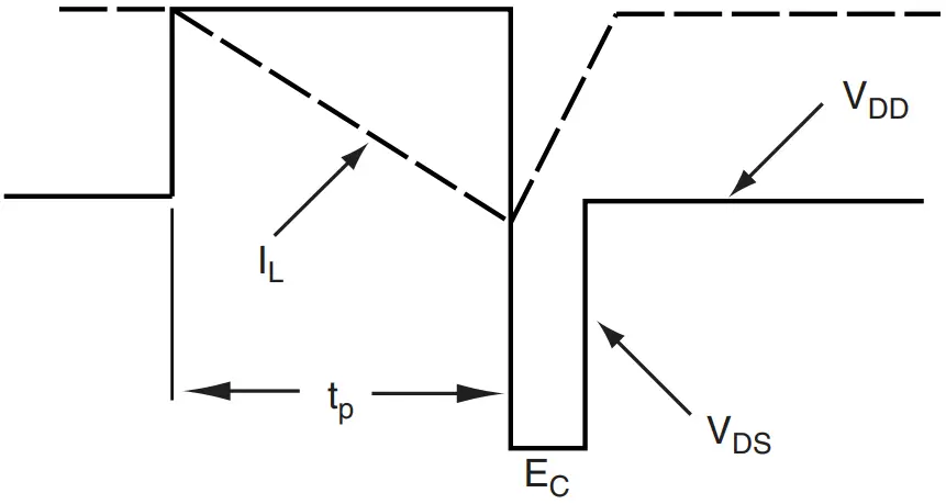
Fig. 17a – Switching Time Test Circuit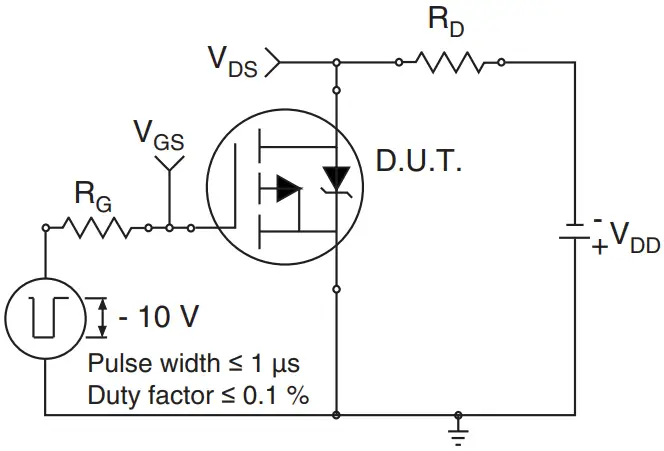
Fig. 17b – Switching Time Waveforms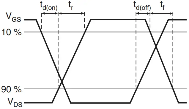
Fig. 18a – Basic Gate Charge Waveform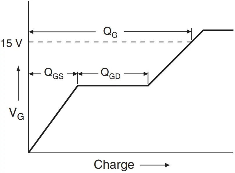
Fig. 18b – Gate Charge Test Circuit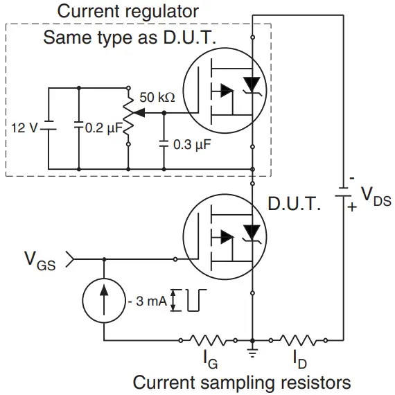
Peak Diode Recovery dV/dt Test Circuit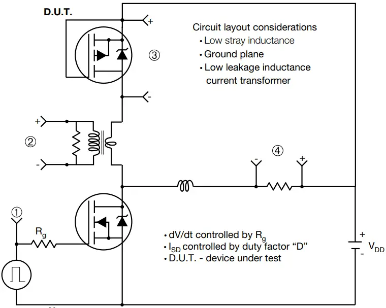
Note
- Compliment N-Channel of D.U.T. for driver
Fig. 19 – For P-Channel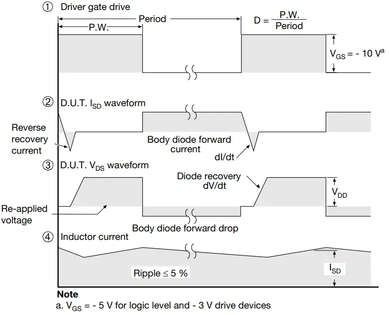
Note
- VGS = – 5 V for logic level and – 3 V drive devices
Vishay Siliconix maintains worldwide manufacturing capability. Products may be manufactured at one of several qualified locations. Reliability data for Silicon Technology and Package Reliability represent a composite of all qualified locations. For related documents such as package/tape drawings, part marking, and
reliability data, see www.vishay.com/ppg?91080.
Package Information
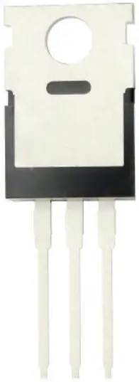
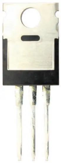
TO-220-1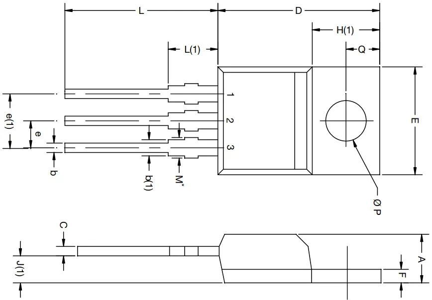
| DIM. | MILLIMETERS | INCHES | ||
| MIN. | MAX. | MIN. | MAX. | |
| A | 4.24 | 4.65 | 0.167 | 0.183 |
| b | 0.69 | 1.02 | 0.027 | 0.040 |
| b(1) | 1.14 | 1.78 | 0.045 | 0.070 |
| c | 0.36 | 0.61 | 0.014 | 0.024 |
| D | 14.33 | 15.85 | 0.564 | 0.624 |
| E | 9.96 | 10.52 | 0.392 | 0.414 |
| e | 2.41 | 2.67 | 0.095 | 0.105 |
| e(1) | 4.88 | 5.28 | 0.192 | 0.208 |
| F | 1.14 | 1.40 | 0.045 | 0.055 |
| H(1) | 6.10 | 6.71 | 0.240 | 0.264 |
| J(1) | 2.41 | 2.92 | 0.095 | 0.115 |
| L | 13.36 | 14.40 | 0.526 | 0.567 |
| L(1) | 3.33 | 4.04 | 0.131 | 0.159 |
| Ø P | 3.53 | 3.94 | 0.139 | 0.155 |
| Q | 2.54 | 3.00 | 0.100 | 0.118 |
| ECN: X15-0364-Rev. C, 14-Dec-15 DWG: 6031 | ||||
Note
- M* = 0.052 inches to 0.064 inches (dimension including protrusion), heatsink hole for HVM
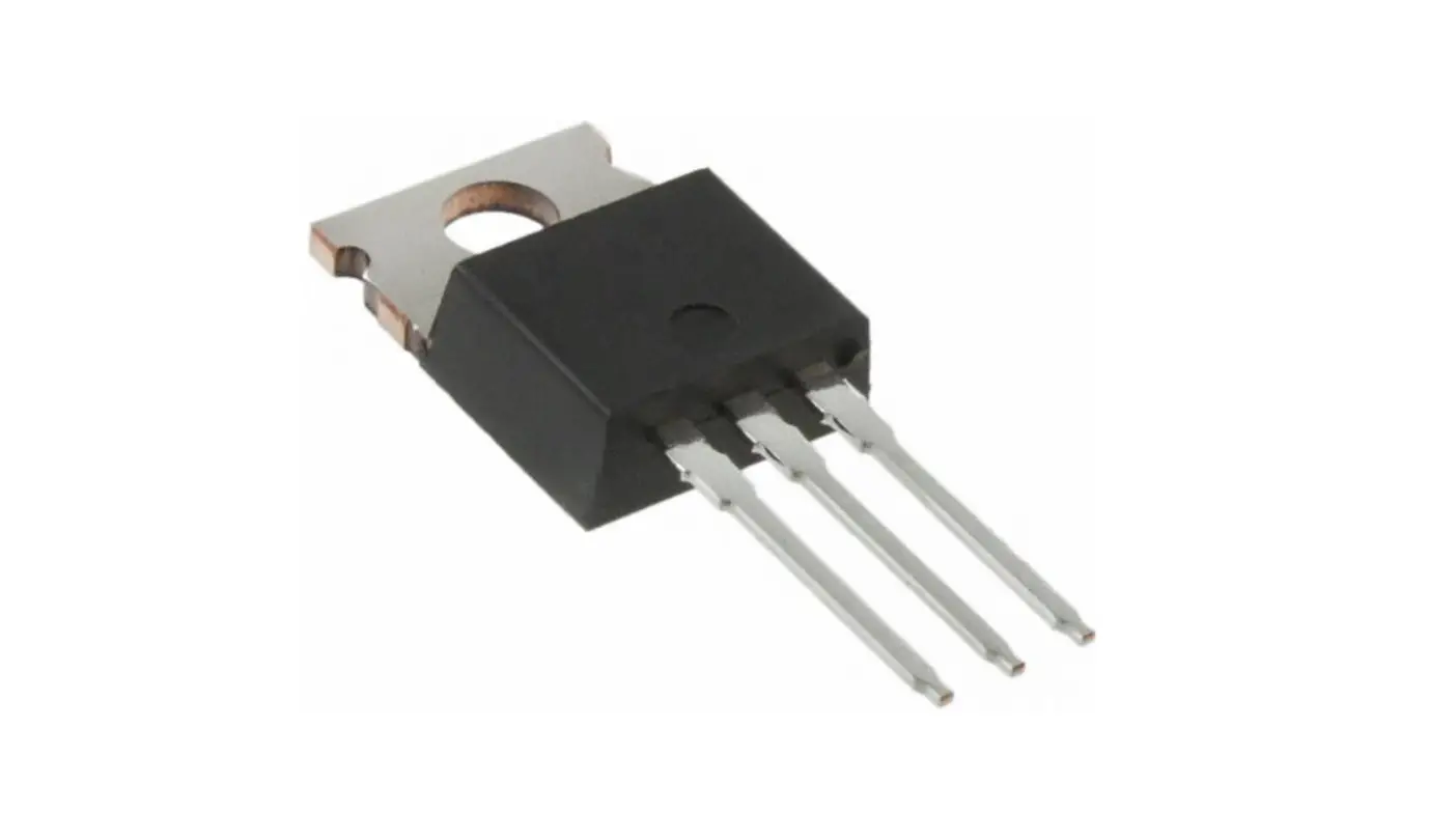
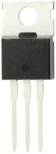
Package Picture
ASE | Xi’an | ||
|
|
|
|
Disclaimer
ALL PRODUCT, PRODUCT SPECIFICATIONS AND DATA ARE SUBJECT TO CHANGE WITHOUT NOTICE TO IMPROVE RELIABILITY, FUNCTION OR DESIGN OR OTHERWISE.
Vishay Inter technology, Inc., its affiliates, agents, and employees, and all persons acting on its or their behalf (collectively, “Vishay”), disclaim any and all liability for any errors, inaccuracies or incompleteness contained in any datasheet or in any other disclosure relating to any product.
Vishay makes no warranty, representation or guarantee regarding the suitability of the products for any particular purpose or the continuing production of any product. To the maximum extent permitted by applicable law, Vishay disclaims (i) any and all liability arising out of the application or use of any product, (ii) any and all liability, including without limitation special, consequential or incidental damages, and (iii) any and all implied warranties, including warranties of fitness for particular purpose, non-infringement and merchantability.
Statements regarding the suitability of products for certain types of applications are based on Vishay’s knowledge of typical requirements that are often placed on Vishay products in generic applications. Such statements are not binding statements about the suitability of products for a particular application. It is the customer’s responsibility to validate that a particular product with the properties described in the product specification is suitable for use in a particular application. Parameters provided in datasheets and / or specifications may vary in different applications and performance may vary over time. All operating parameters, including typical parameters, must be validated for each customer application by the customer’s technical experts. Product specifications do not expand or otherwise modify Vishay’s terms and conditions of purchase, including but not limited to the warranty expressed therein.
Hyperlinks included in this datasheet may direct users to third-party websites. These links are provided as a convenience and for informational purposes only. Inclusion of these hyperlinks does not constitute an endorsement or an approval by Vishay of any of the products, services or opinions of the corporation, organization or individual associated with the third-party website. Vishay disclaims any and all liability and bears no responsibility for the accuracy, legality or content of the third-party website or for that of subsequent links.
Except as expressly indicated in writing, Vishay products are not designed for use in medical, life-saving, or life-sustaining applications or for any other application in which the failure of the Vishay product could result in personal injury or death. Customers using or selling Vishay products not expressly indicated for use in such applications do so at their own risk. Please contact authorized Vishay personnel to obtain written terms and conditions regarding products designed for such applications.
No license, express or implied, by estoppel or otherwise, to any intellectual property rights is granted by this document or by any conduct of Vishay. Product names and markings noted herein may be trademarks of their respective owners.


