VISHAY IRFR420 Siliconix Power MOSFET Instruction Manual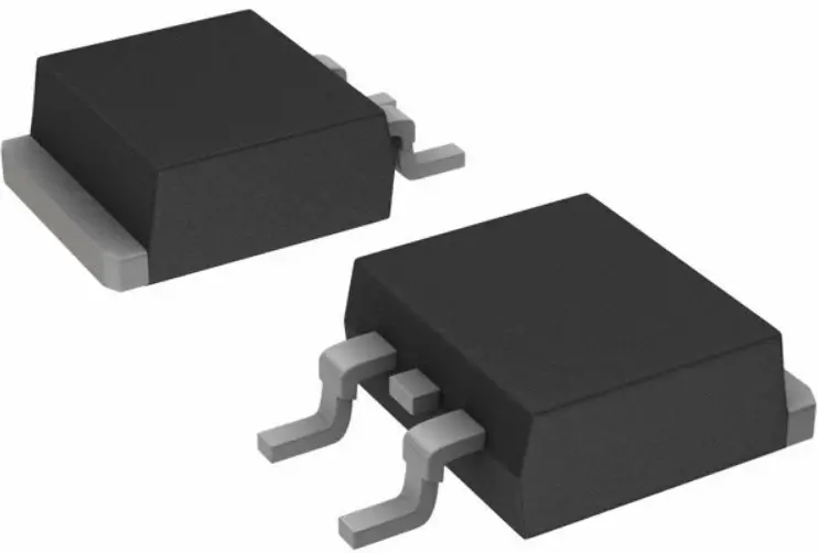
Power MOSFET
| PRODUCT SUMMARY | ||
| VDS (V) | 500 | |
| RDS(on) (L) | VGS = 10 V | 3.0 |
| Qg max. (nC) | 19 | |
| Qgs (nC) | 3.3 | |
| Qgd (nC) | 13 | |
| Configuration | Single | |
FEATURES
- Dynamic dV/dt rating
- Repetitive avalanche rated
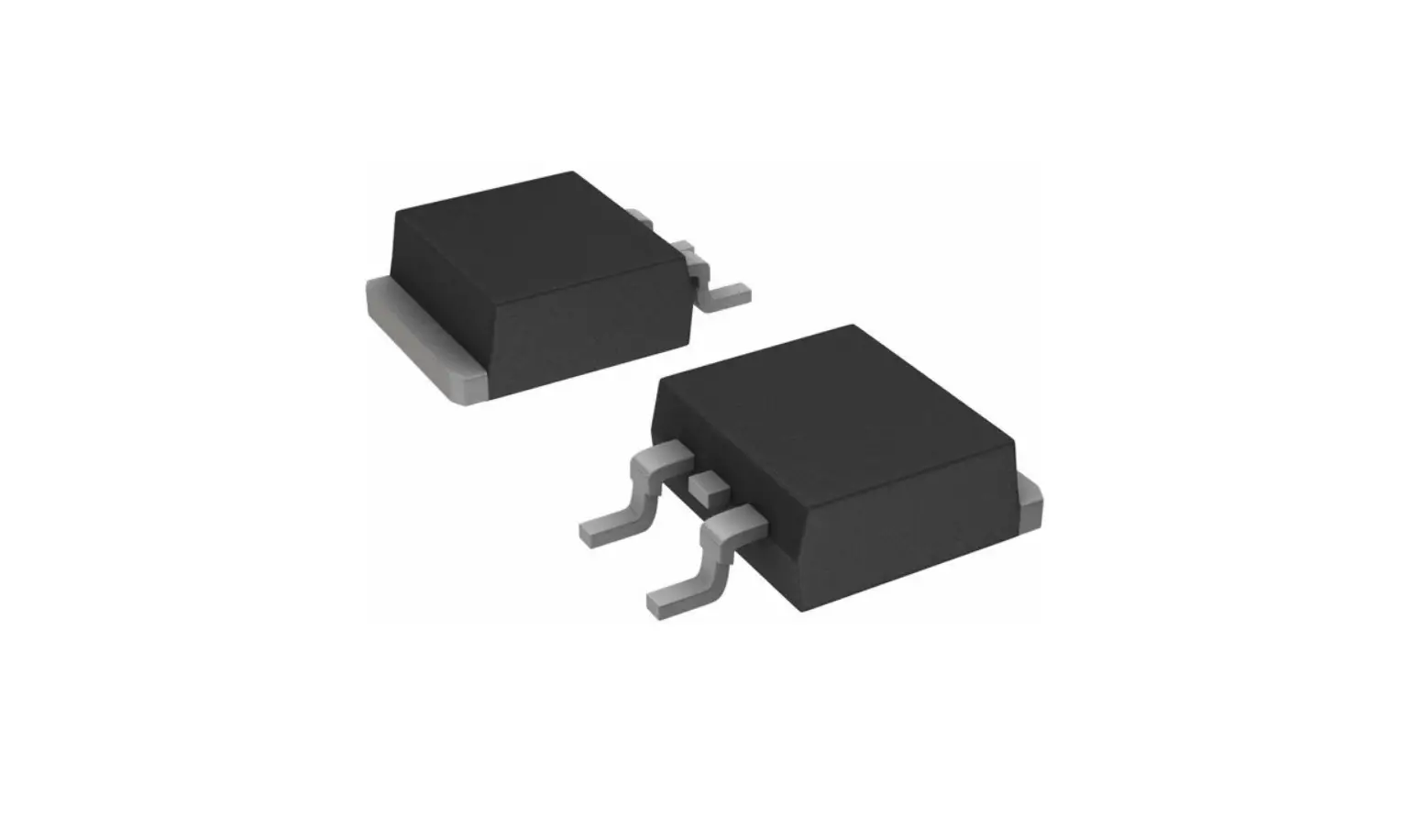
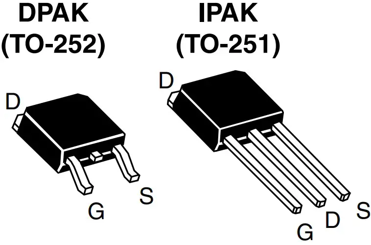
- Surface-mount (IRFR420, SiHFR420)
- Straight lead (IRFU420, SiHFU420)
- Available in tape and reel
- Fast switching
- Ease of paralleling
- Material categorization: for definitions of compliance please see www.vishay.com/doc?99912
DESCRIPTION
Third generation power MOSFETs from Vishay provide the designer with the best combination of fast switching, ruggedized device design, low on-resistance and cost-effectiveness. The DPAK is designed for surface mounting using vapor phase, infrared, or wave soldering techniques. The straight lead version (IRFU, SiHFU series) is for through-hole mounting applications. Power dissipation levels up to 1.5 W are possible in typical surface-mount applications.
| ORDERING INFORMATION | |||||
| Package | DPAK (TO-252) | DPAK (TO-252) | DPAK (TO-252) | DPAK (TO-252) | IPAK (TO-251) |
| Lead (Pb)-free and halogen-free | SiHFR420-GE3 | SiHFR420TR-GE3 a | SiHFR420TRL-GE3 a | SiHFR420TRR-GE3 a | SiHFU420-GE3 |
| IRFR420PbF-BE3 | IRFR420TRPbF-BE3 | IRFR420TRLPbF-BE3 | – | – | |
| Lead (Pb)-free | IRFR420PbF | IRFR420TRPbF a | IRFR420TRLPbF a | IRFR420TRRPbF a | IRFU420PbF |
Note
a. See device orientation
| ABSOLUTE MAXIMUM RATINGS (TC = 25 °C, unless otherwise noted) | |||||
| PARAMETER | SYMBOL | LIMIT | UNIT | ||
| Drain-source voltage | VDS | 500 | V | ||
| Gate-source voltage | VGS | ± 20 | |||
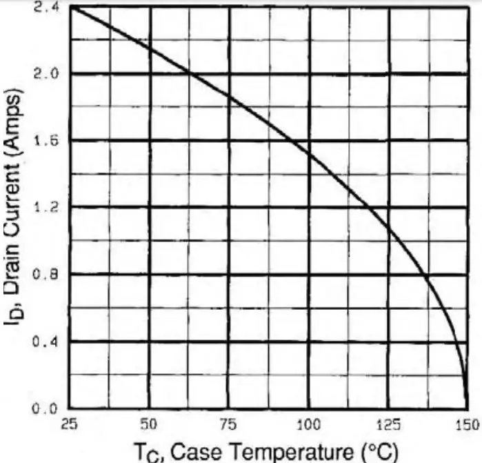
| Continuous drain current | VGS at 10 V | TC = 25 °C | ID | 2.4 | A |
| TC = 100 °C | 1.5 | ||||
| Pulsed drain current a | IDM | 8.0 | |||
| Linear derating factor | 0.33 | W/°C | |||
| Linear derating factor (PCB mount) e | 0.020 | ||||
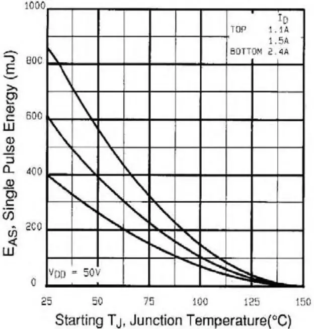
| Single pulse avalanche energy b | EAS | 400 | mJ | ||
| Repetitive avalanche current a | IAR | 2.4 | A | ||
| Repetitive avalanche energy a | EAR | 4.2 | mJ | ||
| Maximum power dissipation | TC = 25 °C | PD | 42 | W | |
| Maximum power dissipation (PCB mount) e | TA = 25 °C | 2.5 | |||
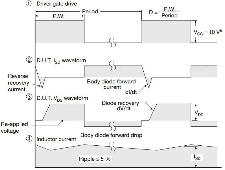
| Peak diode recovery dV/dt c | dV/dt | 3.5 | V/ns | ||
| Operating junction and storage temperature range | TJ, Tstg | -55 to +150 | °C | ||
| Soldering recommendations (peak temperature) d | For 10 s | 260 | |||
Notes
a. Repetitive rating; pulse width limited by maximum junction temperature (see fig. 11)
b. VDD = 50 V, starting TJ = 25 °C, L = 124 mH, Rg = 25 Ω, IAS = 2.4 A (see fig. 12)
c. ISD ≤ 2.4 A, dI/dt ≤ 50 A/μs, VDD ≤ VDS, TJ ≤ 150 °C
d. 1.6 mm from case
e. When mounted on 1″ square PCB (FR-4 or G-10 material)
| THERMAL RESISTANCE RATINGS | ||||
| PARAMETER | SYMBOL | TYP | MAX. | UNIT |
| Maximum junction-to-ambient | RthJA | – | 110 | °C/W |
| Maximum junction-to-ambient (PCB mount) a | RthJA | – | 50 | |
| Maximum junction-to-case (drain) | RthJC | – | 3.0 | |
Note
a. When mounted on 1″ square PCB (FR-4 or G-10 material)
| SPECIFICATIONS (TJ = 25 °C, unless otherwise noted) | |||||||
| PARAMETER | SYMBOL | TEST CONDITIONS | MIN. | TYP. | MAX. | UNIT | |
| Static | |||||||
| Drain-source breakdown voltage | VDS | VGS = 0 V, ID = 250 μA | 500 | – | – | V | |
| VDS temperature coefficient | DVDS/TJ | Reference to 25 °C, ID = 1 mA | – | 0.59 | – | V/°C | |
| Gate-source threshold voltage | VGS(th) | VDS = VGS, ID = 250 μA | 2.0 | – | 4.0 | V | |
| Gate-source leakage | IGSS | VGS = ± 20 V | – | – | ± 100 | nA | |
| Zero gate voltage drain current | IDSS | VDS = 500 V, VGS = 0 V | – | – | 25 | μA | |
| VDS = 400 V, VGS = 0 V, TJ = 125 °C | – | – | 250 | ||||
| Drain-source on-state resistance | RDS(on) | VGS = 10 V | ID =1.4 A b | – | – | 3.0 | L |
| Forward transconductance | gfs | VDS = 50 V, ID = 1.4 A | 1.5 | – | – | S | |
| Dynamic | |||||||
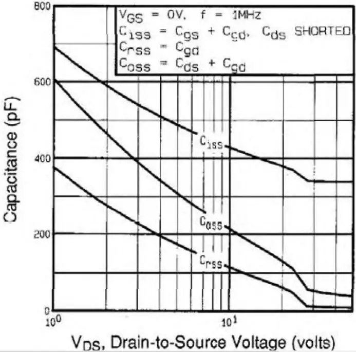
| Input capacitance | Ciss | VGS = 0 V, VDS = 25 V,f = 1.0 MHz, see fig. 5 | – | 360 | – | pF | |
| Output capacitance | Coss | – | 92 | – | |||
| Reverse transfer capacitance | Crss | – | 37 | – | |||
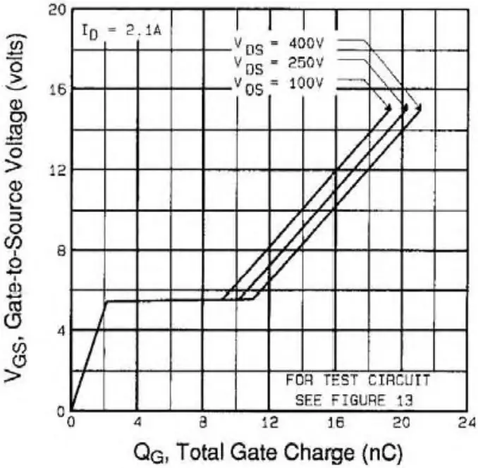
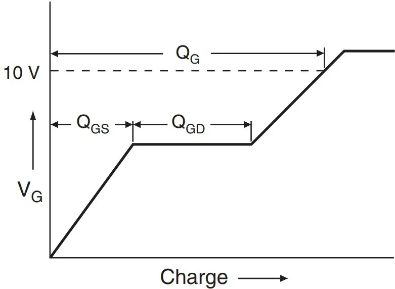
| Total gate charge | Qg | VGS = 10 V | ID = 2.1 A, VDS = 400 V,see fig. 6 and 13 b | – | – | 19 | nC |
| Gate-source charge | Qgs | – | – | 3.3 | |||
| Gate-drain charge | Qgd | – | – | 13 | |||
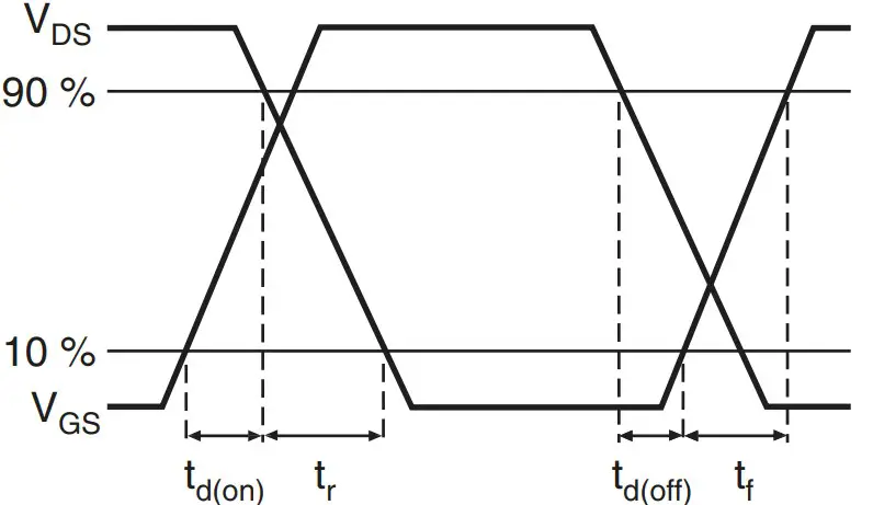
| Turn-on delay time | td(on) | VDD = 250 V, ID = 2.1 A,Rg = 18 L, RD = 120 L, see fig. 10 b | – | 8.0 | – | ns | |
| Rise time | tr | – | 8.6 | – | |||
| Turn-off delay time | td(off) | – | 33 | – | |||
| Fall time | tf | – | 16 | – | |||
| Gate input resistance | Rg | f = 1 MHz, open drain | 1.8 | – | 12.6 | L | |
| Internal drain inductance | LD | Between lead, D6 mm (0.25″) from package and center ofGdie contactS | – | 4.5 | – | nH | |
| Internal source inductance | LS | – | 7.5 | – | |||
| Drain-Source Body Diode Characteristics | |||||||
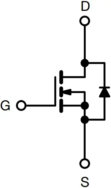
| Continuous source-drain diode current | IS | MOSFET symbolDshowing theintegral reverse Gp – n junction diodeS | – | – | 2.4 | A | |
| Pulsed diode forward current a | ISM | – | – | 8.0 | |||
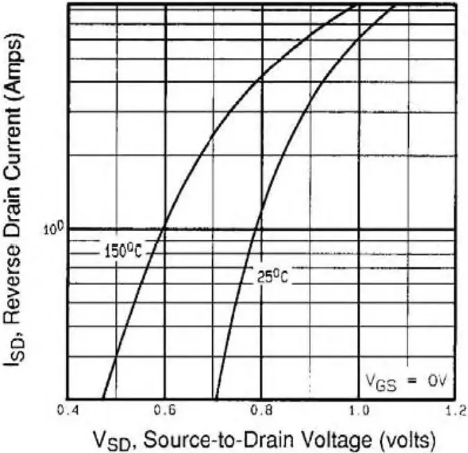
| Body diode voltage | VSD | TJ = 25 °C, IS = 2.4 A, VGS = 0 V b | – | – | 1.6 | V | |
| Body diode reverse recovery time | trr | TJ = 25 °C, IF = 2.1 A, dI/dt = 100 A/μs b | – | 260 | 520 | ns | |
| Body diode reverse recovery charge | Qrr | – | 0.70 | 1.4 | μC | ||
| Forward turn-on time | ton | Intrinsic turn-on time is negligible (turn-on is dominated by LS and LD) | |||||
Notes
a. Repetitive rating; pulse width limited by maximum junction temperature (see fig. 11)
b. Pulse width ≤ 300 μs; duty cycle ≤ 2 %
TYPICAL CHARACTERISTICS (25 °C, unless otherwise noted)
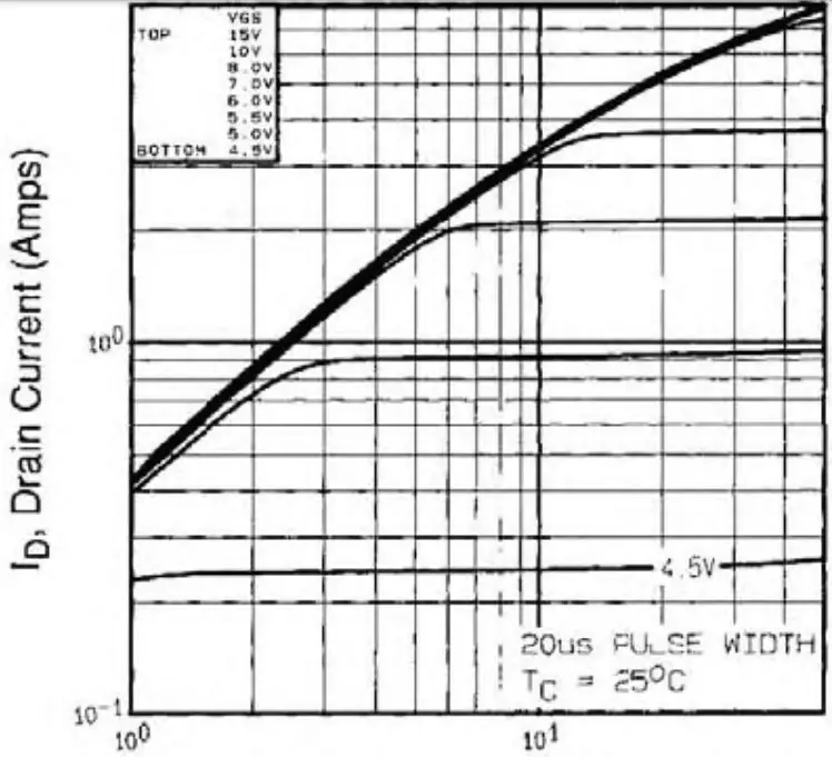
- Typical Output Characteristics, TC = 25 °C

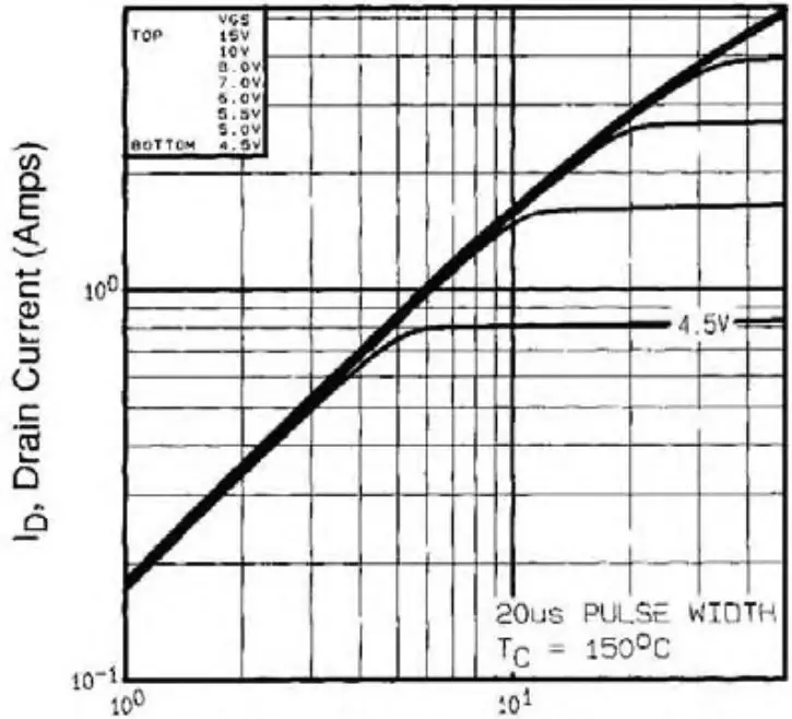
- Typical Output Characteristics, TC = 150 °C

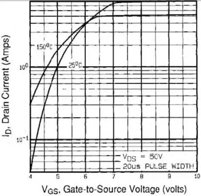
- Typical Transfer Characteristics

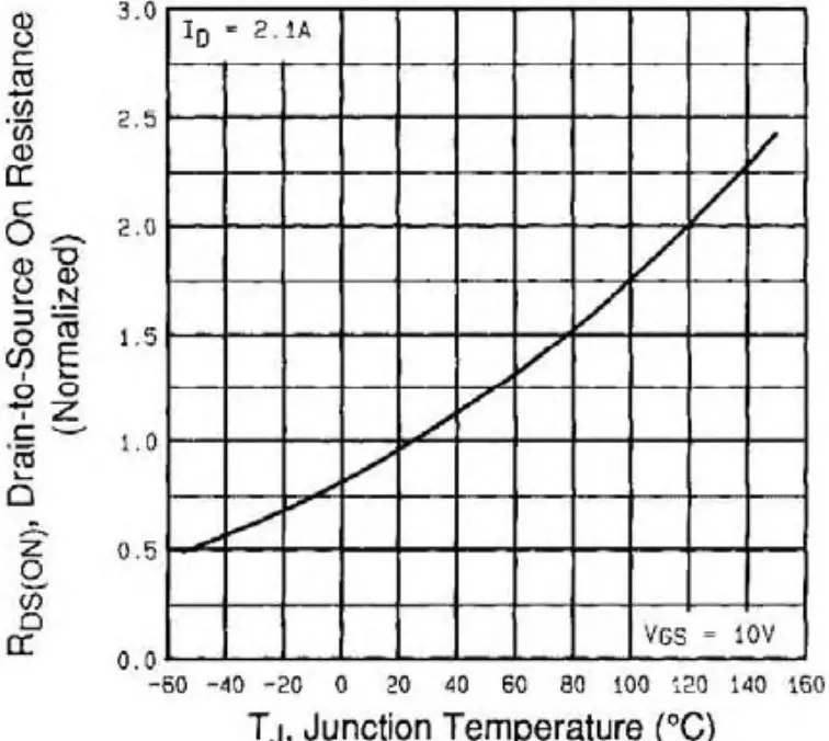
- Normalized On-Resistance vs. Temperature

- Typical Capacitance vs. Drain-to-Source Voltage

- Typical Gate Charge vs. Gate-to-Source Voltage

- Typical Source-Drain Diode Forward Voltage

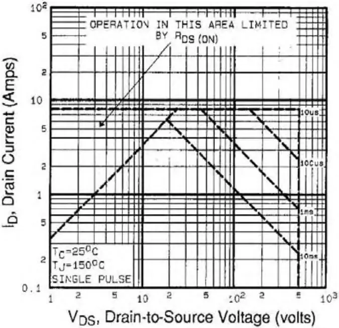
- Maximum Safe Operating Area
- Maximum Drain Current vs. Case Temperature

- Switching Time Waveforms


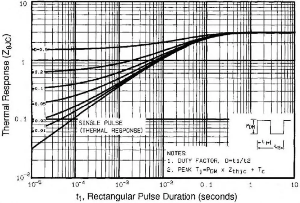
- Maximum Effective Transient Thermal Impedance, Junction-to-Case

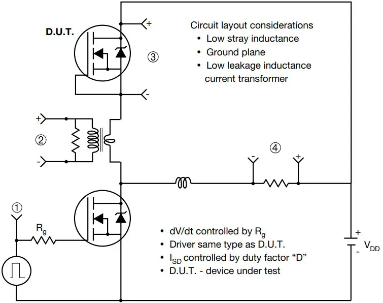
- Unclamped Inductive Test Circuit / Unclamped Inductive Waveforms / Maximum Avalanche Energy vs. Drain Current

- Basic Gate Charge Waveform / Gate Charge Test Circuit


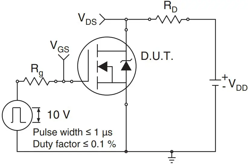
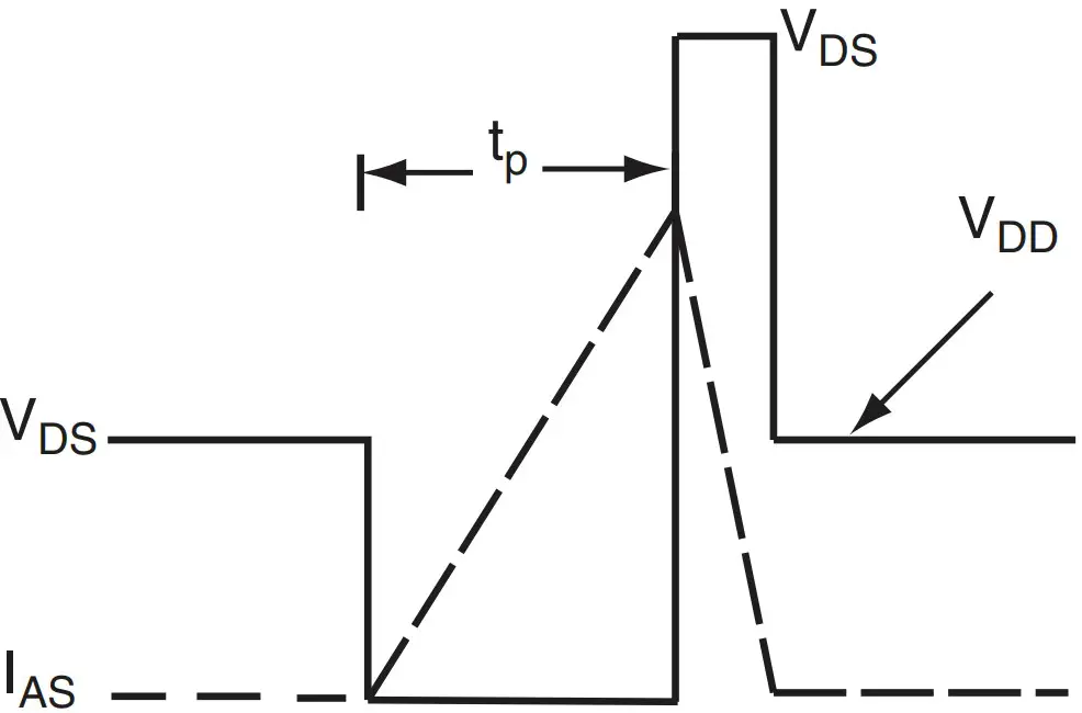
Peak Diode Recovery dV/dt Test Circuit
Driver gate drive
 \
\
VERSION 1: FACILITY CODE = Y
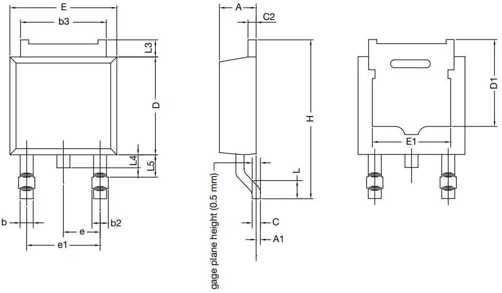
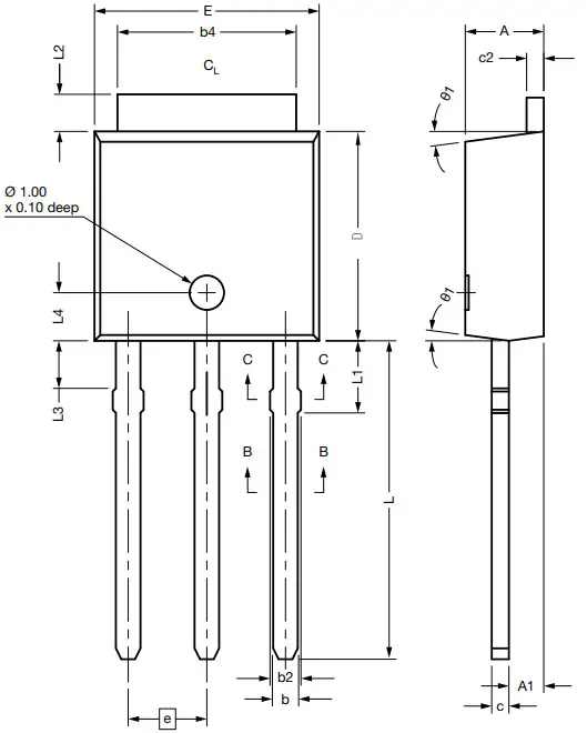
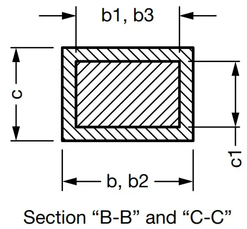
| MILLIMETERS | ||
| DIM. | MIN. | MAX. |
| A | 2.18 | 2.38 |
| A1 | – | 0.127 |
| b | 0.64 | 0.88 |
| b2 | 0.76 | 1.14 |
| b3 | 4.95 | 5.46 |
| C | 0.46 | 0.61 |
| C2 | 0.46 | 0.89 |
| D | 5.97 | 6.22 |
| D1 | 4.10 | – |
| E | 6.35 | 6.73 |
| E1 | 4.32 | – |
| H | 9.40 | 10.41 |
| e | 2.28 BSC | |
| e1 | 4.56 BSC | |
| L | 1.40 | 1.78 |
| L3 | 0.89 | 1.27 |
| L4 | – | 1.02 |
| L5 | 1.01 | 1.52 |
VERSION 2: FACILITY CODE = N
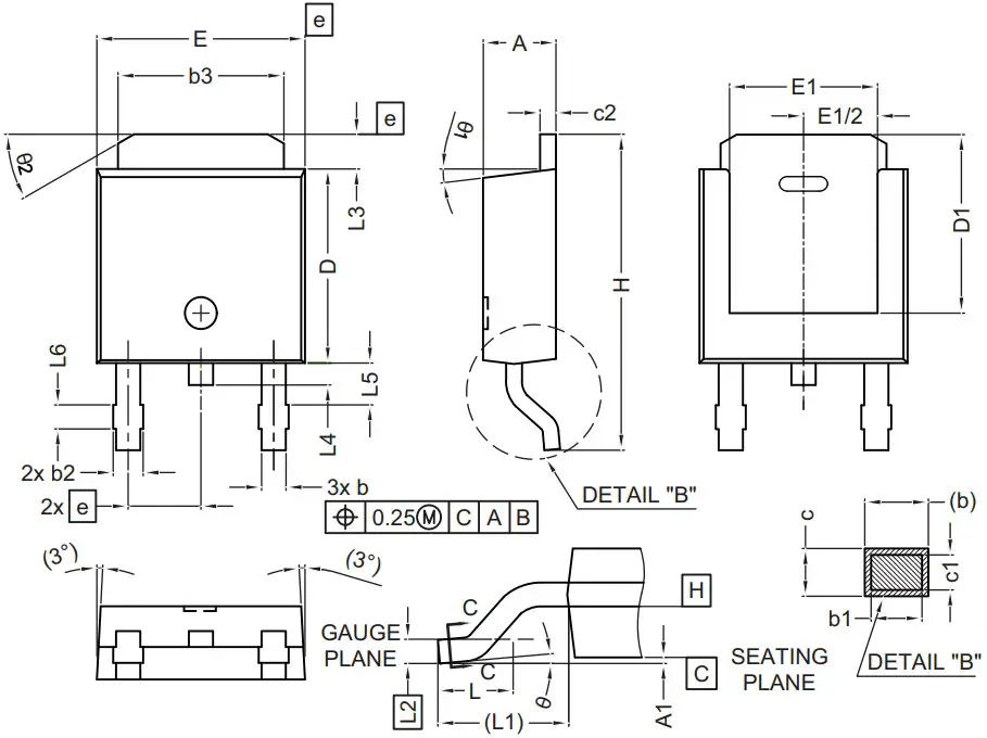
| MILLIMETERS | ||
| DIM. | MIN. | MAX. |
| A | 2.18 | 2.39 |
| A1 | – | 0.13 |
| b | 0.65 | 0.89 |
| b1 | 0.64 | 0.79 |
| b2 | 0.76 | 1.13 |
| b3 | 4.95 | 5.46 |
| c | 0.46 | 0.61 |
| c1 | 0.41 | 0.56 |
| c2 | 0.46 | 0.60 |
| D | 5.97 | 6.22 |
| D1 | 5.21 | – |
| E | 6.35 | 6.73 |
| E1 | 4.32 | – |
| e | 2.29 BSC | |
| H | 9.94 | 10.34 |
| MILLIMETERS | ||
| DIM. | MIN. | MAX. |
| L | 1.50 | 1.78 |
| L1 | 2.74 ref. | |
| L2 | 0.51 BSC | |
| L3 | 0.89 | 1.27 |
| L4 | – | 1.02 |
| L5 | 1.14 | 1.49 |
| L6 | 0.65 | 0.85 |
| q | 0° | 10° |
| q1 | 0° | 15° |
| q2 | 25° | 35° |
Notes
- Dimensioning and tolerance confirm to ASME Y14.5M-1994
- All dimensions are in millimeters. Angles are in degrees
- Heat sink side flash is max. 0.8 mm
- Radius on terminal is optional
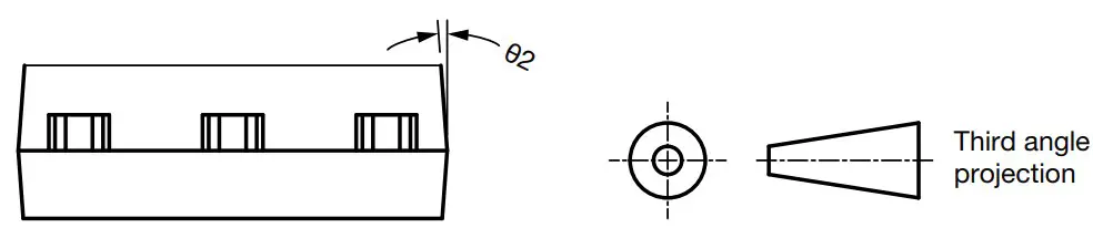
Case Outline for TO-251AA (High Voltage)
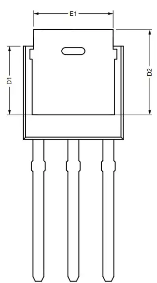
OPTION
| MILLIMETERS | INCHES | MILLIMETERS | INCHES | |||||||
| DIM. | MIN. | MAX. | MIN. | MAX. | DIM. | MIN. | MAX. | MIN. | MAX. | |
| A | 2.18 | 2.39 | 0.086 | 0.094 | D1 | 5.21 | – | 0.205 | – | |
| A1 | 0.89 | 1.14 | 0.035 | 0.045 | E | 6.35 | 6.73 | 0.250 | 0.265 | |
| b | 0.64 | 0.89 | 0.025 | 0.035 | E1 | 4.32 | – | 0.170 | – | |
| b1 | 0.65 | 0.79 | 0.026 | 0.031 | e | 2.29 BSC | 2.29 BSC | |||
| b2 | 0.76 | 1.14 | 0.030 | 0.045 | L | 8.89 | 9.65 | 0.350 | 0.380 | |
| b3 | 0.76 | 1.04 | 0.030 | 0.041 | L1 | 1.91 | 2.29 | 0.075 | 0.090 | |
| b4 | 4.95 | 5.46 | 0.195 | 0.215 | L2 | 0.89 | 1.27 | 0.035 | 0.050 | |
| c | 0.46 | 0.61 | 0.018 | 0.024 | L3 | 1.14 | 1.52 | 0.045 | 0.060 | |
| c1 | 0.41 | 0.56 | 0.016 | 0.022 | q1 | 0′ | 15′ | 0′ | 15′ | |
| c2 | 0.46 | 0.86 | 0.018 | 0.034 | q2 | 25′ | 35′ | 25′ | 35′ | |
| D | 5.97 | 6.22 | 0.235 | 0.245 | ||||||
| ECN: E21-0682-Rev. C, 27-Dec-2021 DWG: 5968 | ||||||||||
Notes
- Dimensioning and tolerancing per ASME Y14.5M-1994
- Dimension are shown in inches and millimeters
- Dimension D and E do not include mold flash. Mold flash shall not exceed 0.13 mm (0.005″) per side. These dimensions are measured at the outermost extremes of the plastic body
- Thermal pad contour optional with dimensions b4, L2, E1 and D1
- Lead dimension uncontrolled in L3
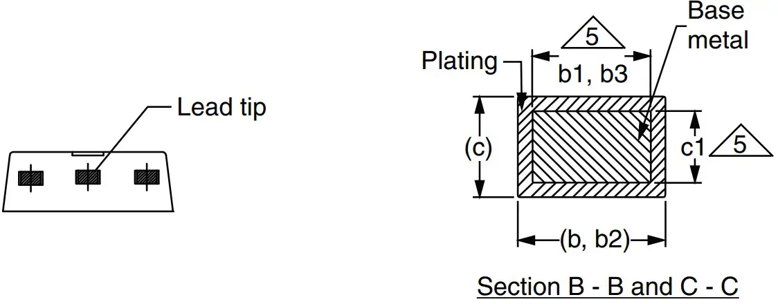
- Dimension b1, b3 and c1 apply to base metal only
- Outline conforms to JEDEC® outline TO-251AA
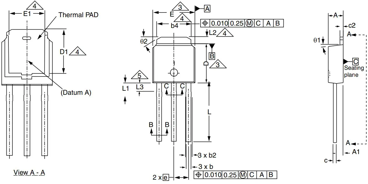
OPTION 2: FACILITY CODE = N
| DIM. | MIN. | NOM. | MAX. | DIM. | MIN. | NOM. | MAX. | |
| A | 2.180 | 2.285 | 2.390 | D2 | 5.380 | – | – | |
| A1 | 0.890 | 1.015 | 1.140 | E | 6.350 | 6.540 | 6.730 | |
| b | 0.640 | 0.765 | 0.890 | E1 | 4.32 | – | – | |
| b1 | 0.640 | 0.715 | 0.790 | e | 2.29 BSC | |||
| b2 | 0.760 | 0.950 | 1.140 | L | 8.890 | 9.270 | 9.650 | |
| b3 | 0.760 | 0.900 | 1.040 | L1 | 1.910 | 2.100 | 2.290 | |
| b4 | 4.950 | 5.205 | 5.460 | L2 | 0.890 | 1.080 | 1.270 | |
| c | 0.460 | – | 0.610 | L3 | 1.140 | 1.330 | 1.520 | |
| c1 | 0.410 | – | 0.560 | L4 | 1.300 | 1.400 | 1.500 | |
| c2 | 0.460 | – | 0.610 | q1 | 0° | 7.5° | 15° | |
| D | 5.970 | 6.095 | 6.220 | q2 | 4° | – | – | |
| D1 | 4.300 | – | – | |||||
| ECN: E21-0682-Rev. C, 27-Dec-2021 DWG: 5968 | ||||||||
Notes
- Dimensioning and tolerancing per ASME Y14.5M-1994
- All dimension are in millimeters, angles are in degrees
- Heat sink side flash is max. 0.8 mm
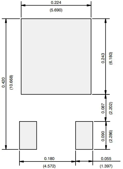
RECOMMENDED MINIMUM PADS FOR DPAK (TO-252)
Disclaimer
ALL PRODUCT, PRODUCT SPECIFICATIONS AND DATA ARE SUBJECT TO CHANGE WITHOUT NOTICE TO IMPROVE RELIABILITY, FUNCTION OR DESIGN OR OTHERWISE. Vishay Intertechnology, Inc., its affiliates, agents, and employees, and all persons acting on its or their behalf (collectively, “Vishay”), disclaim any and all liability for any errors, inaccuracies or incompleteness contained in any datasheet or in any other disclosure relating to any product.Vishay makes no warranty, representation or guarantee regarding the suitability of the products for any particular purpose or the continuing production of any product. To the maximum extent permitted by applicable law, Vishay disclaims (i) any and all liability arising out of the application or use of any product, (ii) any and all liability, including without limitation special, consequential or incidental damages, and (iii) any and all implied warranties, including warranties of fitness for particular purpose, non-infringement and merchantability.
Statements regarding the suitability of products for certain types of applications are based on Vishay’s knowledge of typical requirements that are often placed on Vishay products in generic applications. Such statements are not binding statements about the suitability of products for a particular application. It is the customer’s responsibility to validate that a particular product with the properties described in the product specification is suitable for use in a particular application. Parameters provided in datasheets and / or specifications may vary in different applications and performance may vary over time. All operating parameters, including typical parameters, must be validated for each customer application by the customer’s technical experts. Product specifications do not expand or otherwise modify Vishay’s terms and conditions of purchase, including but not limited to the warranty expressed therein.
Hyperlinks included in this datasheet may direct users to third-party websites. These links are provided as a convenience and for informational purposes only. Inclusion of these hyperlinks does not constitute an endorsement or an approval by Vishay of any of the products, services or opinions of the corporation, organization or individual associated with the third-party website. Vishay disclaims any and all liability and bears no responsibility for the accuracy, legality or content of the third-party website or for that of subsequent links. Except as expressly indicated in writing, Vishay products are not designed for use in medical, life-saving, or life-sustaining applications or for any other application in which the failure of the Vishay product could result in personal injury or death. Customers using or selling Vishay products not expressly indicated for use in such applications do so at their own risk. Pleasecontact authorized Vishay personnel to obtain written terms and conditions regarding products designed for such applications.No license, express or implied, by estoppel or otherwise, to any intellectual property rights is granted by this document or by any conduct of Vishay. Product names and markings noted herein may be trademarksof their respective owners.


