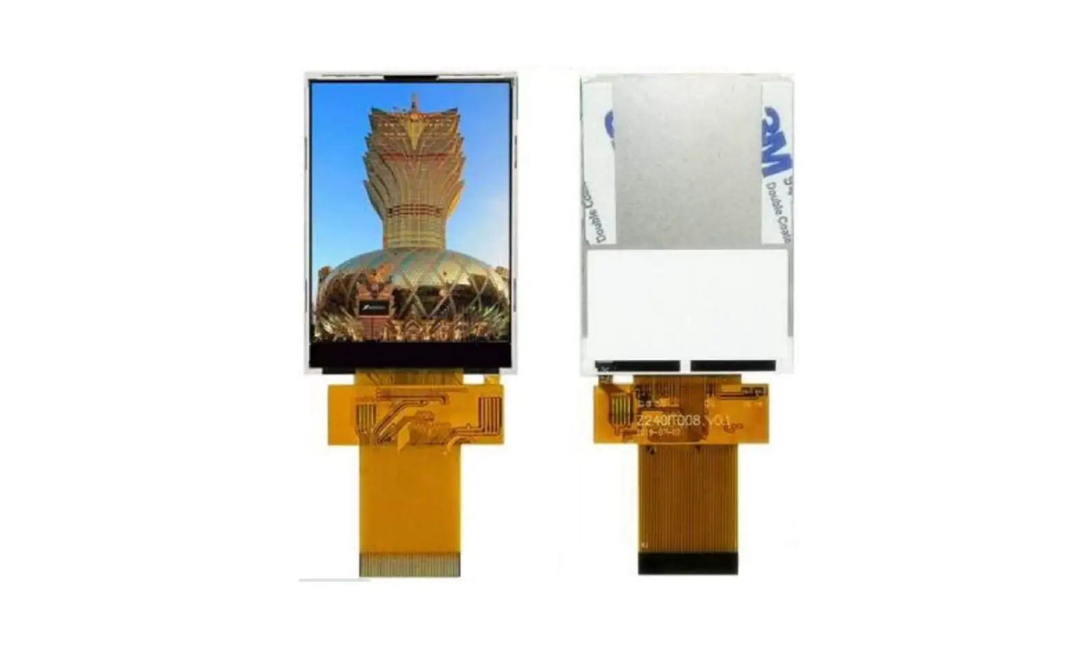
Surenoo STP0240D1-240320 Series TFT LCD Panel User Manual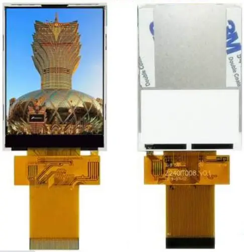
Contents hide
General Description
| MODEL NO | STP0240D1-240320 YT240L008 |
| Display Mode | Transmissive |
| Display Format | Graphic 240RGB*320 Dot-matrix 240xRGBx320 |
| Input Data | 4 Line-SPI/8bit/16bit interface 4 |
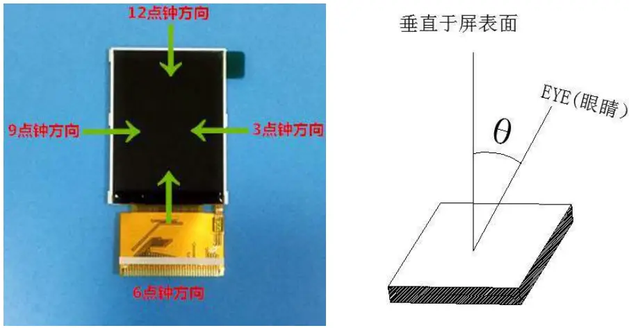
| Viewing Direction | 12 o’clock 12 |
| Drive | ILI9341 |
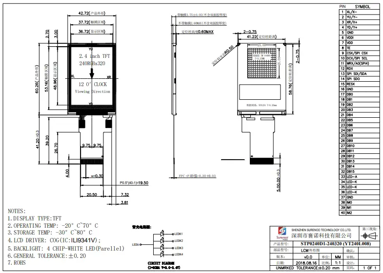
Mechanical Specification
| Item | Specifications | Unit |
| Dimensional outline | 42.72(W)*60.26(H)*2.55(T)(NTP)42.72(W)*60.26(H)*3.75(T)(RTP) (FPC not include) | mm |
| Resolution | 240RGB*320 | dots |
| LCD Active area | 36.72(W)*48.96 (H) | mm |
| Pixel size | 0.153(W)*0.153(H) | mm |
Mechanical Dimension
Electrical Maximum Ratings
| Item | Symbol | Min | Max | Unit | Note |
| Supply voltag(VDDI) | V | 1.8 | 3.3 | V | – |
| Supply voltage(VDD ) | V | 2.8 | 3.3 | V | – |
| Operating temperature | TOPR | -20 | 70 | ℃ | – |
| Storage temperature | TSTR | -30 | 80 | ℃ | – |
Brightness characteristic&Power dissipation
| Item | Symbol | Min | Typical | Max | Unit |
| LED module Forward voltage | VLED | 2.9 | 3.1 | 3.3 | V |
| LED module current | ILED | – | 60 | – | mA |
| LCD Surface Luminance | LS | 250 | 300 | – | Cd/m2 |
| LCM Surface brightness uniform | LD | 80 | – | – | % |
| LCD power dissipation | PLCD | – | 0.22 | – | W |
NOTE:PLCD=VDD * (ILED+ILCD)
Module Function Description
| PIN No. | Symbol | Description | Notes |
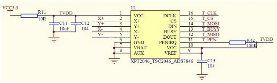
| 1 | XL(X-) | Touch panel Logical foot | – |
| 2 | YU(Y+) | Touch panel Logical foot | – |
| 3 | XR(X+) | Touch panel Logical foot | – |
| 4 | YD(Y+) | Touch panel Logical foot | – |
| 5 | GND | Ground | – |
| 6 | VDDI | Power Supply for I/O System. | – |
| 7 | VDD | Power Supply for Analog, Digital System and Booster Circuit. | – |
| 8 | TE | Tearing effect signal is used to synchronize MCU to frame memory | – |
| 9 | CSX/SPI CSX |
| – |
| 10 | DCX/SPI SCL |
| 复用脚 |
| 11 | WRX/A0(SPI4) |
| 复用脚 |
| 12 | RDX |
| – |
| 13 | SPI SDI/SDA | SPI interface input pin.
| – |
| 14 | SPI SDO |
| – |
| 15 | RESX |
| – |
| 16 | GND | Ground | – |
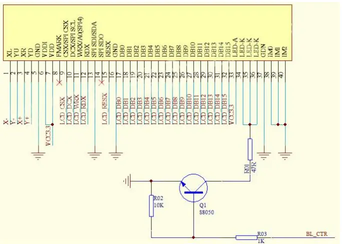
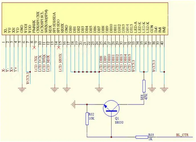
| 17-24 | DB0-DB7 | MCU parallel interface data bus. | – |
| 25-32 | DB8-DB15 | MCU parallel interface data bus. | – |
| 33 | LED-A | Anode of Backlight (2.9V-3.3V Typical:3.1V) | – |
| 34-36 | LED-K | Cathode of Backlight | – |
| 37 | GND | Ground | – |
| 38 | IM0 | -The MCU interface mode select. | – |
| 39 | IM1 | 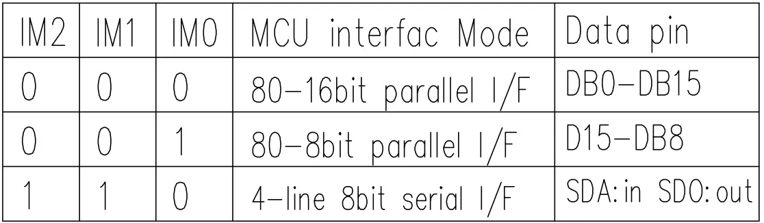 | – |
| 40 | IM2 | *NOTE:,IM3。 | – |
Wiring

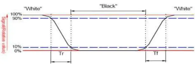
Response time&Contrast ratio
| Item | Symbol | Condition | Remark | Unit | ||
| Min. | Typ. | Max. | ||||
| Response time | Tr+Tf | θ=0° | – | 25 | 40 | ms |
| Contrast ratio | CR | θ=0° | 350 | 500 | – | – |
Viewing Angle
| Item | Symbol | Condition | Remark | Unit | ||
| Min. | Typ. | Max. | ||||
| Viewing angle | Top 12 | CR≥10 | 40 | 50 | – | Deg. |
| Bottom 6 | CR≥10 | 55 | 65 | – | ||
| Left 9 | CR≥10 | 55 | 65 | – | ||
| Right 3 | CR≥10 | 55 | 65 | – | ||
Reliability Trial
| NO. | ITEM | CONDITION | CRITERION |
| 1 | High Temperature Non-Operating Test | 80℃*120Hrs | No Defect Of Operational Function In Room Temperature Are Allowable |
| 2 | Low Temperature Non-Operating Test | -30℃*120Hrs | |
| 3 | High Temperature/Humidity Non Operating Test | 60℃*90%RH*120Hrs | |
| 4 | High Temperature Operating Test | 70℃*72Hrs | |
| 5 | Low Temperature Operating Test | -20℃*72Hrs | |
| 6 | Thermal Shock Test | -20 ℃ (30Min) Q70 ℃ (30Min) *10CYCLES |
Inspection standard
Glass defect
| NO | Defect item | Criteria | Remark |
| 1 | Dimension Unconformity (Major defect) | By Engineering Drawing | |
| 2 | Cracks (Major defect) | 1.Linear cracks panel【Reject】 2. Nonlinear crack contrast by limited sample |  |
| 3 | Glass extrude the conductive area (minor defect) | a: disregards and no influence assemblage.
| A: Length, b: Width |
| 4 | Pin-side ,conductive area damaged (minor defect) | (a c: disregards) b≤1/3of effective length for bonding electrode【Accept】 | a: length, b: Width, c: Thickness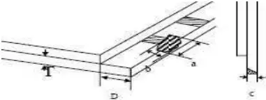 |
| 5 | Pin-side,non-conductive area damaged (minor defect) | 1) Damage area don’t touch the ITO (Inclueling contraposition mark, except scribing mark) 【Accept】 2) C<T b≦BM1/3of width 【Accept】 3) c=T b not touch the seal glue 【Accept】 4) a disregards | a: Length, b: Width c: Thickness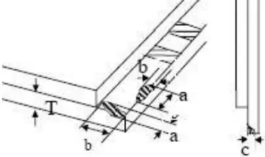 |
| 6 | Non-pin-side damage (minor defect) | c<T 1)b exceeds 1/3Bm 【Reject】 c=T b not touch the seal glue 【Reject】 | c: Thickness b: width of damage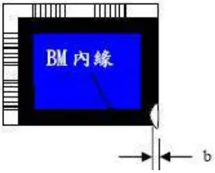 |
LCD appearance defect(View area)
| NO | Defect item | Criteria | Remark | |
| 1 | Fiber glass cratch polarizer scratch/folded (minor defect) | Specification | Allowable | note1:L: Length, W: Width note2: disregard if out of AA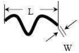
|
| W≦0.03mm | disregard | |||
| 0.03mm<W≦0.05mm; L≦3.0mm | 2 | |||
| 0.05mm<W≦0.1mm; L≦3.0mm | 1 | |||
| W>0.1mm;L>3.0mm | 0 | |||
| 2 | Polarizer bubble、concave and convex (minor defect) | φ≦0.2mm | disregard | note1: φ=(L+W)/2,L:Length, W :Width note2:disregard if out of AA |
| 0.2mm<φ≦0.3mm | 2 | |||
| 0.3mm<φ≦0.5mm | 1 | |||
| 0.5mm<φ | 0 | |||
| 3 | Black dots dirty dots impurities eye winker (minor defect) | φ≦0.15mm | disregard | note2:disregard if out of AA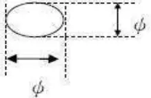 |
| 0.15mm<φ≦0.25mm | 2 | |||
| 0.25mm<φ≦0.3mm | 1 | |||
| 0.3mm<φ | 0 | |||
| 4 | Polarizer prick (minor defect) | φ≦0.1mm | disregard | note1: φ=(L+W)/2,L=Length, W=Width note2:the distance between two dots>5mm |
| 0.1mm<φ≦0.25mm | 3 | |||
| φ>0.25mm | 0 | |||
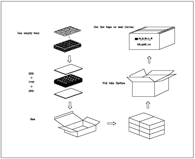
Package Method