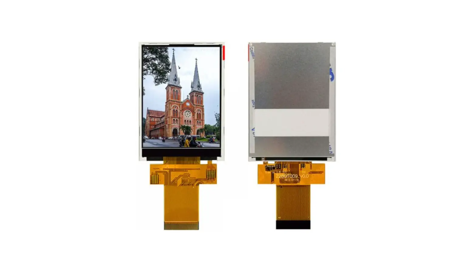
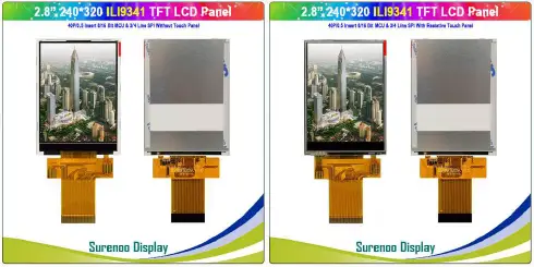
STP0280D1-240320 Series TFT LCD Panel
 OLOGY CO.,LTD.
A3 Model No.: STP0280D1-240320
STP0280D1-240320 Series
TFT LCD PANEL USER MANUAL
Please click the following image to buy the sample

Shenzhen Surenoo Technology Co.,Ltd.
www.surenoo.com
Skype: Surenoo365
Reference Controller Datasheet
TFT LCD Panel Selection Guide
ILI9341
1. General Description
| MODEL NO | STP0280D1-240320 YT280L008 | |
| Display Mode | Transmissive | |
| Display Format | Graphic 240R | 1.General Description |
| Input Data | 4 Line-SPI/8bit | |
| Viewing Direction | 12 o’clock | |
| Drive | ILI9341 | |
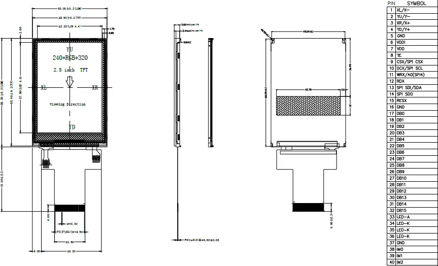
2. Mechanical Specification
| Item | Specifications | Unit |
| Dimensional outline | 50.00(W)*69.20(H)*2.60(T)(NTP) 50.00(W)*69.20(H)*3.80(T)(RTP) (FPC not include) | mm |
| Resolution | 240RGB*320 | dots |
| LCD Active area | 36.72(W)*48.96 (H) | mm |
| Pixel size | 0.153(W)*0.153(H) | mm |
3.Mechanical Dimension
NOTES:
1.DISPLAY TYPE:TFT
2.OPERATING TEMP: -20°C~70°C
3.STORAGE TEMP: -30°C~80°C
4.LCD DRIVER: COG(IC:ILI9341V);
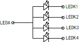
5.BACKLIGHT: 4 CHIP-WHITE LED(Parellel)
6.GENERAL TOLERANCE:±0.20
7.ROHS
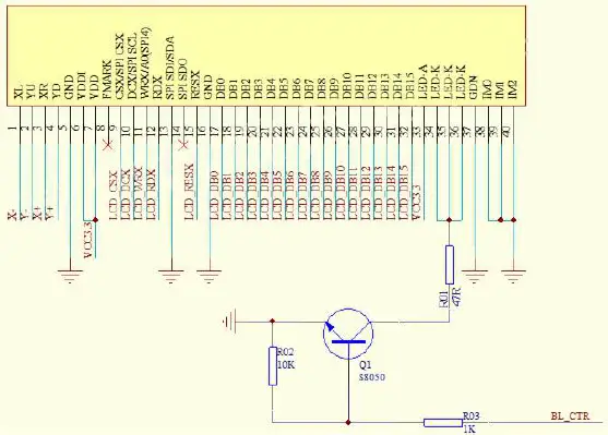
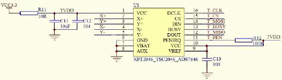
CIRCUIT DIAGRAM
4. Electrical Maximum Ratings
| Item | Symbol | Min | Max | Unit | Note |
| Supply voltage(VDDI) | V | 1.8 | 3.3 | V | – |
| Supply voltage(VDD) | V | 2.8 | 3.3 | V | – |
| Operating temperature | TOPR | -20 | 70 | ℃ | – |
| Storage temperature | TSTR | -30 | 80 | ℃ | – |
5. Brightness characteristic & Power dissipation
| Item | Symbol | Min | Typical | Max | Unit |
| LED module Forward voltage | VLED | 2.9 | 3.1 | 3.3 | V |
| LED module current | ILED | – | 60 | – | mA |
| LCD Surface Luminance | LS | 250 | 300 | – | Cd/m2 |
| LCM Surface brightness uniform | LD | 80 | – | – | % |
| LCD power dissipation | PLCD | – | 0.22 | – | W |
NOTE: PLCD=VDD * (ILED+ILCD)
6. Module Function Description
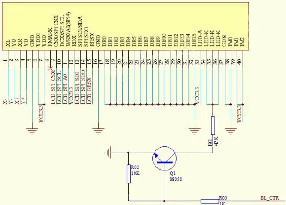
| PIN No. | Symbol | Description panel Logical foot | Notes |
| 1 | XL(X-) | Touch panel Logical foot | – |
| 2 | YU(Y+) | Touch panel Logical foot | – |
| 3 | XR(X+) | Touch panel Logical foot | – |
| 4 | YD(Y+) | Touch panel Logical foot | – |
| 5 | GND | Ground | – |
| 6 | VDDI | Power Supply for I/O System. | – |
| 7 | VDD | Power Supply for Analog, Digital System and Booster Circuit. | – |
| 8 | TE | Tearing effect signal is used to synchronize MCU to frame memory | – |
| 9 | DCX/SPI SCL | -Chip selection pin Low enable. High disable. | – |
| 10 | DCX/SPI SCL | -Display data/command selection pin in parallel interface. -This pin is used to be serial interface clock. | |
| 11 | WRX/A0(SPI4) | -Write enable in MCU parallel interface. – Display data/command selection pin in 4-line serial interface. | |
| 12 | RDX | -If not used, please fix this pin at VDDI or GND. -Read interface input pin. | – |
| 13 | SPI SDI/SDA | SPI interface input pin. -The data is latched on the rising edge of the SCL signal. -If not used, please fix this pin at VDDI or DGND level. | – |
| 14 | SPI SDO | -SPI interface output pin. -The data is output on the falling edge of the SCL signal. -If not used, let this pin open. | – |
| 15 | RESX | -This signal will reset the device and it must be applied to properly initialize the chip. -Signal is active low. | – |
| 16 | GND | Ground | – |
| 17-24 | DB0-DB7 | MCU parallel interface data bus. | – |
| 25-32 | DB8-DB15 | MCU parallel interface data bus. | – |
| 33 | LED-A | Anode of Backlight (2.9V-3.3V Typical:3.1V) | – |
| 34-36 | LED-K | Cathode of Backlight | – |
| 37 | GND | Ground | – |
38 39 40 | IM0 | -The MCU interface mode select. | – |
| IM1 | 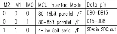 | – | |
| IM2 | *NOTE: | – |
STP0280D1 MCU-16
6-1: STP0280D1 MCU-8
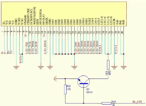
6-2 STP0280D1 4-W SPI
6-3
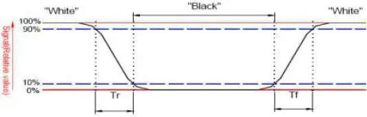
7.Response time & Contrast ratio
Item | Symbol | Condition | Remark | Unit | ||
| Min. | Typ. | Max. | ||||
| Response time | Tr+Tf | θ=0° | – | 25 | 40 | ms |
| Contrast ratio | CR | θ=0° | 350 | 500 | – | – |

8. Viewing Angle
Item | Symbol | Condition | Remark | Unit | ||
| Min. | Typ. | Max. | ||||
Viewing angle | Top | CR≥10 | 40 | 50 | – | Deg. |
| Bottom | CR≥10 | 55 | 65 | – | ||
| Left | CR≥10 | 55 | 65 | – | ||
| Right | CR≥10 | 55 | 65 | – | ||
9. Reliability Trial
| NO. | ITEM | CONDITION | CRITERION |
| 1 | High Temperature Non-Operating Test | 80℃*120Hrs | No Defect Of Operational Function In Room Temperature Are Allowable |
| 2 | Low Temperature Non-Operating Test | -30℃*120Hrs Remark | |
| 3 | High Temperature/Humidity Non Operating Test | 60℃*90%RH*120Hrs | |
| 4 | High Temperature Operating Test | 70℃*72Hrs | |
| 5 | Low Temperature Operating Test | -20℃*72Hrs℃ (30Min) | |
| 6 | Thermal Shock Test | -20 Q70℃(30Min) *10CYCLES |
10.Inspection standards
10.1Glass defect
| NO | Defect item | Criteria | Remark |
| 1 | Dimension Unconformity (Major defect) | By Engineering Drawing | |
| 2 | Cracks (Major defect) | 1. Linear cracks panel 【Reject】 2. Nonlinear crack contrast by limited sample |  |
| 3 | Glass extrude the conductive area (minor defect) | a: disregards and no influence assemblage. 1) b≤1/3Pin width(non bonding area) 【Accept】 2)bonding area≤0.5mm 【Accept】 | A: Length, b: Width |
| 4 | Pin-side ,conductive area damaged (minor defect) | (a c: disregards) b≤1/3of effective length for bonding electrode 【Accept】 | a: length, b: Width, c: Thickness  |
| 5 | Pin-side,non-conductive area damaged (minor defect) | 1)Damage area don’t touch the ITO (Inclueling contraposition mark, except scribing mark) 【Accept】 2)C<T b≦BM1/3of width 【Accept】 3)c=T b not touch the seal glue 【Accept】 4)a disregards | a: Length, b: Width c: Thickness 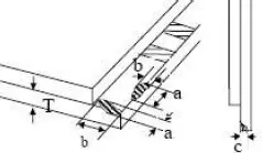 |
| 6 | Non-pin-side damage (minor defect) | c<T 1)b exceeds 1/3Bm 【Reject】 c=T b not touch the seal glue 【Reject】 | c: Thickness b: width of damage 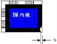 |
10.2LCD appearance defect(View area)
| NO | Defect item | Criteria | Remark | |
1 | Fiber、glass | Specification | Allowable | note2:disregard if out of AA note2:disregard if out of AA 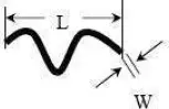 |
| cratch、polarizer | W≦0.03mm | disregard | ||
| scratch/folded | 0.03mm<W≦0.05mm; L≦3.0mm | 2 disregard | ||
| (minor defect) | 0.05mm<W≦0.1mm; L≦3.0mm | 1 | ||
W>0.1mm;L>3.0mm | ||||
2 | 、Polarizer bubble、 concave and convex (minor defect) | φ≦0.2mm | disregard | note1: φ=(L+W)/2,L:Length, W :Width note2:disregard if out of AA |
| 0.2mm<φ≦0.3mm | 2 | |||
| 0.3mm<φ≦0.5mm | 1 | |||
| 0.5mm<φ φ≦ | 0 | |||
| 3 | Black dots、dirty dots、 | 0.15mm | disregard | note2:disregard if out of AA |
impurities、eye winker (minor defect) | 0.15mm<φ≦0.25mm | 2 | |
| 0.25mm<φ≦0.3mm | 1 | ||
| 0.3mm<φ | 0 | ||
4 | Polarizer prick (minor defect) | φ≦0.1mm | note1: φ=(L+W)/2,L=Length, W=Width note2:the distance between two dots>5mm |
| 0.1mm<φ≦0.25mm | |||
| φ>0.25mm |
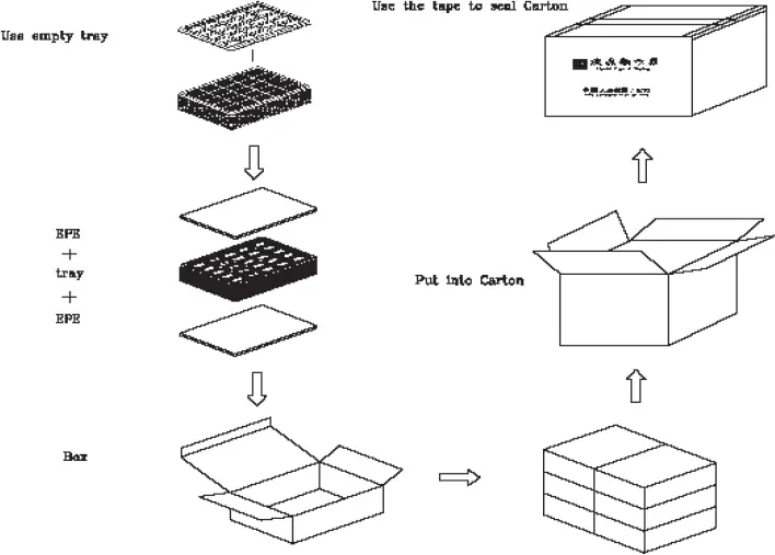
11.Package Method