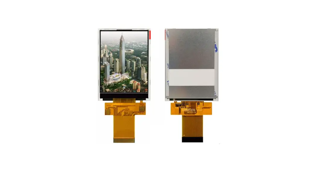
![]() STP0280D2-240320 Series TFT LCD Panel
STP0280D2-240320 Series TFT LCD Panel
User Manual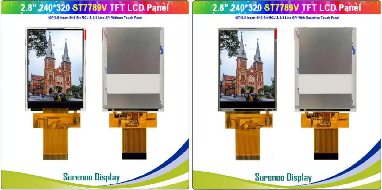 https://www.aliexpress.com/item/4000529764310.html
General Description
| MODEL NO | STP0280D2-240320 YT280L008 |
| Display Mode | Transmissive |
| Display Format | Graphic 240RGB*320 Dot-matrix 240xRGBx320 |
| Input Data | 4 Line-SPI/8bit/16bit interface 4 |
| Viewing Direction | 12 o’clock |
| Drive | ST7789V |
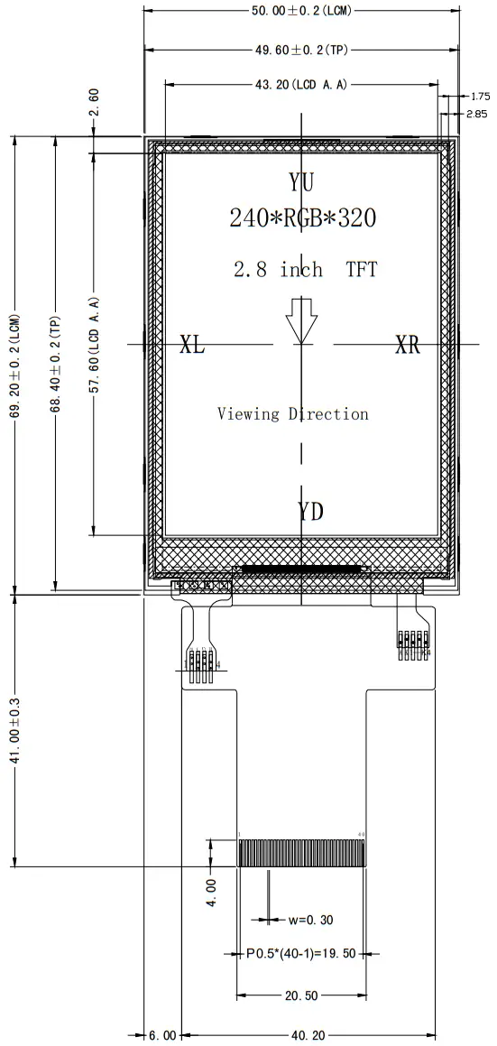
Mechanical Specification
| Item | Specifications | Unit |
| Dimensional outline | 50.00(W)*69.20(H)*2.60(T)(NTP) 50.00(W)*69.20(H)*3.80(T)(RTP) (FPC not include) | mm |
| Resolution | 240RGB*320 | dots |
| LCD Active area | 36.72(W)*48.96 (H) | mm |
| Pixel size | 0.153(W)*0.153(H) | mm |
Mechanical Dimension
 NOTES:
- DISPLAY TYPE:TFT
- OPERATING TEMP: -20°C~70°C
- STORAGE TEMP: -30°C~80°C
- LCD DRIVER: COG(IC:ST7789V);
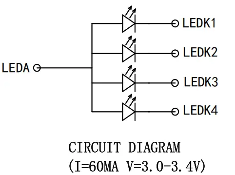
- BACKLIGHT: 4 CHIP-WHITE LED(Parellel)
- GENERAL TOLERANCE: ±0.20
- ROHS


| PIN | SYMBOL | PIN | SYMBOL |
| 1 | XL/X- | 21 | DB4 |
| 2 | YU/Y- | 22 | DB5 |
| 3 | XR/X+ | 23 | DB6 |
| 4 | YD/Y+ | 24 | DB7 |
| 5 | GND | 25 | DB8 |
| 6 | VDDI | 26 | DB9 |
| 7 | VDD | 27 | DB10 |
| 8 | TE | 28 | DB11 |
| 9 | CSX/SPI CSX | 29 | DB12 |
| 10 | DCX/SPI SCL | 30 | DB13 |
| 11 | WRX/A0(SP14) | 31 | DB14 |
| 12 | RDX | 32 | DB15 |
| 13 | SPI SDI/SDA | 33 | LED-A |
| 14 | SPI SDO | 34 | LED-K |
| 15 | RESX | 35 | LED-K |
| 16 | GND | 36 | LED-K |
| 17 | DB0 | 37 | GND |
| 18 | DB1 | 38 | IMO |
| 19 | DB2 | 39 | IM1 |
| 20 | DB3 | 40 | IM2 |
| Third Perspective: | |||||
| Product number: | STP0280D2-240320 (YT280S008) | ||||
| Part Model: | LCM Outline | confirm: | |||
| Version: | v0.0 | unit: | MM | Audit: | |
| date: | 2018.08.16 | Proportion: | 1:01 | design: | |
| UNMRKED TOLERANCE: +0.20 mm | page number: | 1 OF 1 | |||
Electrical Maximum Ratings
| Item | Symbol | Min | Max | Unit | Note |
| Supply voltage (VDDI) | V | 1.8 | 3.3 | V | – |
| Supply voltage (VDD) | V | 2.8 | 3.3 | V | – |
| Operating temperature 1 | TOPR | -20 | 70 | °C | – |
| Storage temperature | TSTR | -30 | 80 | °C | – |
※NOTE: VDDI and VDD can be directly connected together and share a set of voltage (2.8V~3.3V) for power supply.
Brightness characteristic & Power dissipation
| Item | Symbol | Min | Typical | Max | Unit |
| LED module Forward voltage | V LED | 2.9 | 3.1 | 3.3 | V |
| LED module current | I LED | – | 60 | – | mA |
| LCD Surface Luminance | Ls | 250 | 300 | – | Cd/m² |
| LCM Surface brightness uniform | L D | 80 | – | – | % |
| LCD power dissipation | P LCD | – | 0.22 | – | W |
※NOTE: PLCD=VDD * (I LED+I LCD)
Module Function Description
| PIN No. | Symbol | Description | Notes | ||||||||||||||||||||
| 1 | XL(X-) | Touch panel Logical foot | – | ||||||||||||||||||||
| 2 | YU(Y+) | Touch panel Logical foot | – | ||||||||||||||||||||
| 3 | XR(X+) | Touch panel Logical foot | – | ||||||||||||||||||||
| 4 | YD(Y+) | Touch panel Logical foot | – | ||||||||||||||||||||
| 5 | GND | Ground | – | ||||||||||||||||||||
| 6 | VDDI | Power Supply for I/O System. | – | ||||||||||||||||||||
| 7 | VDD | Power Supply for Analog, Digital System and Booster Circuit. | – | ||||||||||||||||||||
| 8 | TE | Tearing effect signal is used to synchronize MCU to frame memory | – | ||||||||||||||||||||
| 9 | CSX/SPI CSX | -Chip selection pin Low enable. High disable. | – | ||||||||||||||||||||
| 10 | DCX/SPI SCL | -Display data/command selection pin in parallel interface. -This pin is used to be serial interface clock. | – | ||||||||||||||||||||
| 11 | WRX/A0(SPI4) | -Write enable in MCU parallel interface. – Display data/command selection pin in 4-line serial interface. | – | ||||||||||||||||||||
| 12 | RDX | -Read enable in 8080 MCU parallel interface. -If not used, please fix this pin at VDDI or GND. | – | ||||||||||||||||||||
| 13 | SPI SDI/SDA | SPI interface input pin. -The data is latched on the rising edge of the SCL signal. -If not used, please fix this pin at VDDI or DGND level. | – | ||||||||||||||||||||
| 14 | SPI SDO | -SPI interface output pin. -The data is output on the falling edge of the SCL signal. -If not used, let this pin open. | – | ||||||||||||||||||||
| 15 | RESX | -This signal will reset the device and it must be applied to properly initialize the chip. -Signal is active low. | – | ||||||||||||||||||||
| 16 | GND | Ground | – | ||||||||||||||||||||
| 17-24 | DB0-DB7 | MCU parallel interface data bus. | – | ||||||||||||||||||||
| 25-32 | DB8-DB15 | MCU parallel interface data bus. | – | ||||||||||||||||||||
| 33 | LED-A | Anode of Backlight (2.9V-3.3V Typical:3.1V) | – | ||||||||||||||||||||
| 34-36 | LED-K | Cathode of Backlight | – | ||||||||||||||||||||
| 37 | GND | Ground | – | ||||||||||||||||||||
| 38 | IM0 | -The MCU interface mode select. | – | ||||||||||||||||||||
| 39 | IM1 |
| – | ||||||||||||||||||||
| 40 | IM2 | *NOTE: In the circuit of the display screen, IM3 is fixedly connected to high level. | – |
Figure 6-1: Display screen Bit parallel port reference application circuit STP0280D2 MCU-16
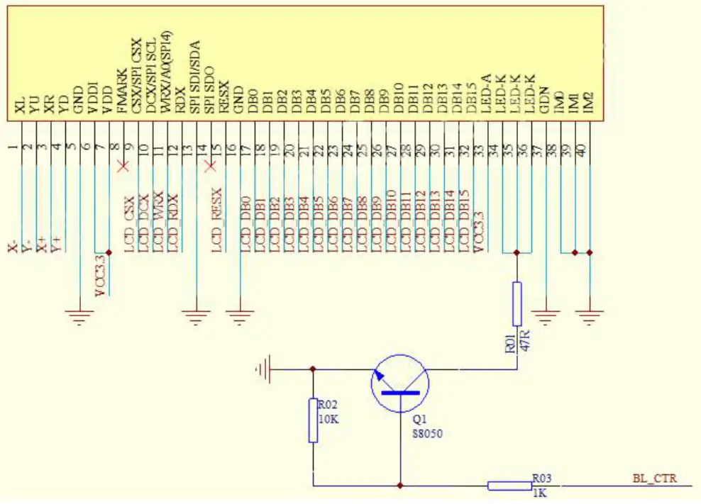 Figure 6-1: Display screen Bit parallel port reference application circuit STP0280D2 MCU-8
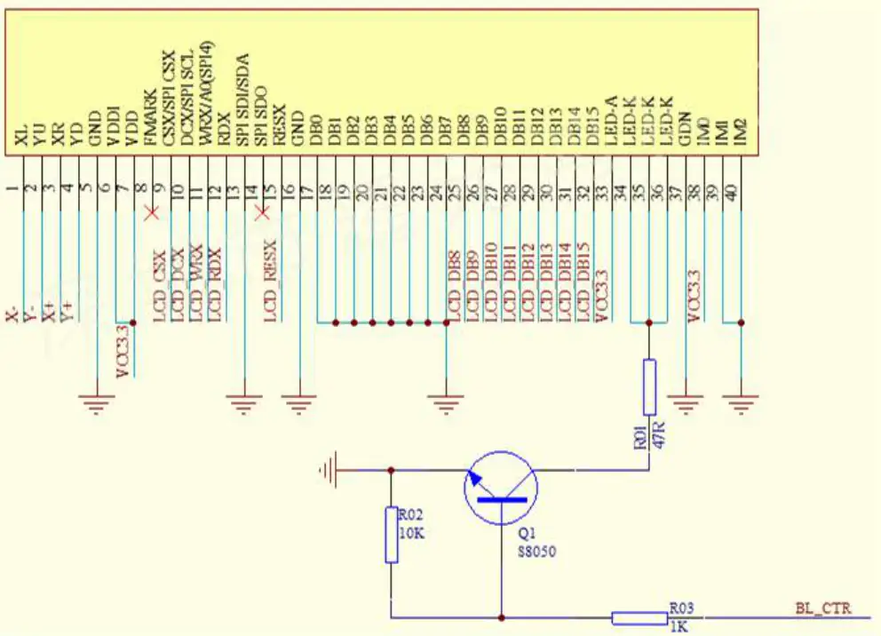
Figure 6-2: Display screen STP0280D2 4-W SPI serial port reference application circuit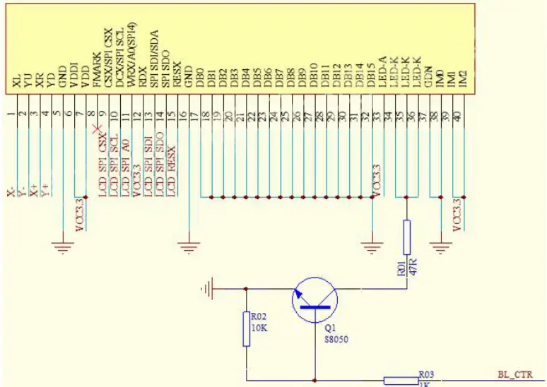
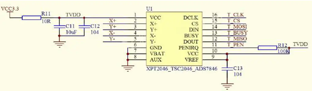
Figure 6-3: Touch screen reference application circuit
※NOTE:
- If it is a version without touch screen, refer to Figure 6-1 or Figure 6-2 to connect the circuit, and connect the XL, YU, XR, YD of the display screen Just touch the foot and hang it in the air.
- For the version with touch, refer to Figure 6-3 Touch Application Connection Circuit.
Response time & Contrast ratio
| Item | Symbol | Condition | Remark | Unit | ||
| Min. | Typ. | Max. | ||||
| Response time | Tr+Tf | θ = 0º | – | 25 | 40 | ms |
| Contrast ratio | CR | θ = 0º | 350 | 500 | – | – |
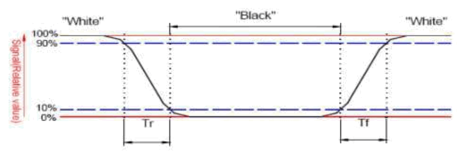 Response time graph
![]() Contrast calculation formula
Contrast calculation formula
Viewing Angle
| Item | Symbol | Condition | Remark | Unit | ||
| Min. | Typ. | Max. | ||||
| Viewing angle | Top | CR ≥ 10 | 40 | 50 | – | Deg. |
| Bottom | CI ≥ 10 | 55 | 65 | – | ||
| Left | CR ≥ 10 | 55 | 65 | – | ||
| Right | CR ≥ 10 | 55 | 65 | – | ||
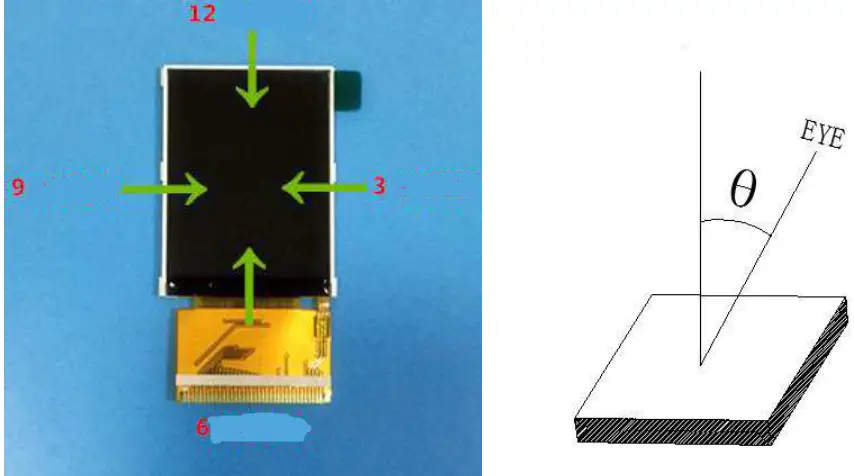
NOTE: The angle of view of 3 o’clock, 6 o’clock, 9 o’clock, and 12 o’clock refers to the angle (0) between the lines perpendicular to the surface of the screen and the line of sight of the eye.
Reliability Trial
| NO. | ITEM | CONDITION | CRITERION |
| 1 | High Temperature Non-Operating Test | 80°C *120Hrs | No Defect Of Operational Function In Room Temperature Are Allowable |
| 2 | Low Temperature Non-Operating Test | -30 C*120Hrs | |
| 3 | High Temperature/Humidity Non Operating Test | 60°C*90%RH*120Hrs | |
| 4 | High Temperature Operating Test | 70°C*72Hrs | |
| 5 | Low Temperature Operating Test | 20°C *72Hrs | |
| 6 | 1 hermal Shock Test | -20°C (30Min) Q 70°C (30Min) *10CYCLES |
Inspection standards
| NO | Defect item | Criteria | Remark |
| 1 | Dimension Unconformity (Major defect) | By Engineering Drawing | |
| 2 | Cracks (Major defect) | 1. Linear cracks panel 【Reject】 2. Nonlinear crack contrast by limited sample | |
| 3 | Glass extrude the conductive area (minor defect) | a: disregards and no influence assemblage. 1) b≤1/3Pin width(non bonding area) 【Accept】 2)bonding area≤0.5mm 【Accept】 | A: Length, b: Width |
| 4 | Pin-side ,conductive area damaged (minor defect) | (a c: disregards) b≤1/3of effective length for bonding electrode 【Accept】 | a: length, b: Width, c: Thickness |
| 5 | Pin-side,non-conductive area damaged (minor defect) | 1)Damage area don’t touch the ITO (Inclueling contraposition mark, except scribing mark) 【Accept】 2)C<T b≦BM1/3of width 【Accept】 3)c=T b not touch the seal glue 【Accept】 4)a disregards | a: Length, b: Width c: Thickness |
| 6 | Non-pin-side damage (minor defect) | c<T 1)b exceeds 1/3Bm 【Reject】 c=T b not touch the seal glue 【Reject】 | c: Thickness b: width of damage |
10.2 LCD appearance defect(View area)
| NO | Defect item | Criteria | Remark | |
| 1 | Fiber, glass cratch, polarizer scratch/folded (minor defect) | Specification | Allowable | note l:L: Length, W: Width note 2: disregard if out of AA |
| W- 0.03mm | disregard | |||
| 0.03mm<W O. 05mm;1_,- 3. Omm | 2 | |||
| 0.05mm<W O. lmm; L-<= 3. Omm | 1 | |||
| W>0.1mm;L>3.0mm | 0 | |||
| 2 | Polarizer bubble, concave and convex (minor defect) | 0.2mm | disregard | note l: (I)= (L+W) /2, L : Length, W :Width note 2:disregard if out of AA |
| 0.2mm< (I) 0. 3mm | 2 | |||
| 0.3mm< (1) 0. 5mm | 1 | |||
| 0.5mm< (1) | 0 | |||
| 3 | Black dots, dirty dots, | (1) 0.15 mm | disregard | note 2:disregard if out of AA |
| impurities, eye winker (minor defect) | 0.15mm< (1) -.. O. 25mm | 2 | ||
| 0.25mm< (1) -.. 0. 3m | 1 | |||
| 0.3mm< (1) | 0 | |||
| 4 | Polarizer prick (minor defect) | (1) 0.1mm | disregard | note 1: (1) = (L+W) /2, L=Length, W=Width note2:the distance between two dots>5mm |
| 0.1mm< (1) 0. 25m | 3 | |||
| (1) >O. 25mm | 0 |
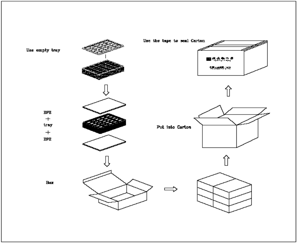
Package Method
 |  |  |
| https://wa.me/qr/4GGOIDYZ2PXXN1 | https://wa.me/qr/4GGOIDYZ2PXXN1 | http://qr.kakao.com/talk/THom9tzJN5OMzvx1vTL1V.LvnEc- |
 |  |
| https://line.me/ti/p/oas8BmVLVd | https://u.wechat.com/EAK0B_l2YfPLwx3tRqiKkf4 |
Shenzhen Surenoo Technology Co.,Ltd.
www.surenoo.com
Skype: Surenoo365


