![]()
SHENZHEN SURENOO TECHNOLOGY CO.,LTD.
Model No.: STP0240E-240320
STP0240E-240320 Series
TFT LCD PANEL USER MANUAL
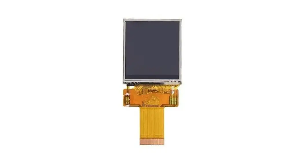
Please click the following image to buy the sample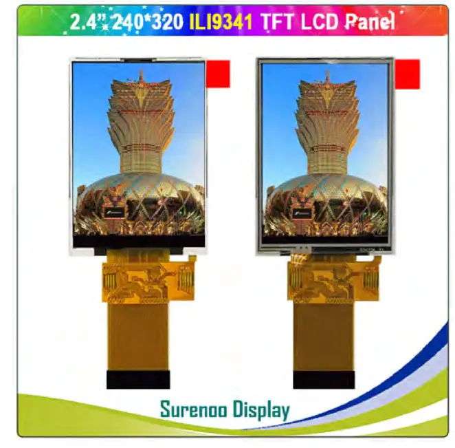
Reference Controller Datasheet
TFT LCD Panel Selection Guide
ILI9341
General Description
| MODEL NO | STP0240E-240320 |
| Display Mode | Transmissive |
| Display Format | Graphic 240RGB*320 Dot-matrix 240xRGBx320 |
| Input Data | 8bit/16bit interface 8 口/16口 |
| Viewing Direction | 12 o’clock 12 |
| Drive | ILI9341 () |
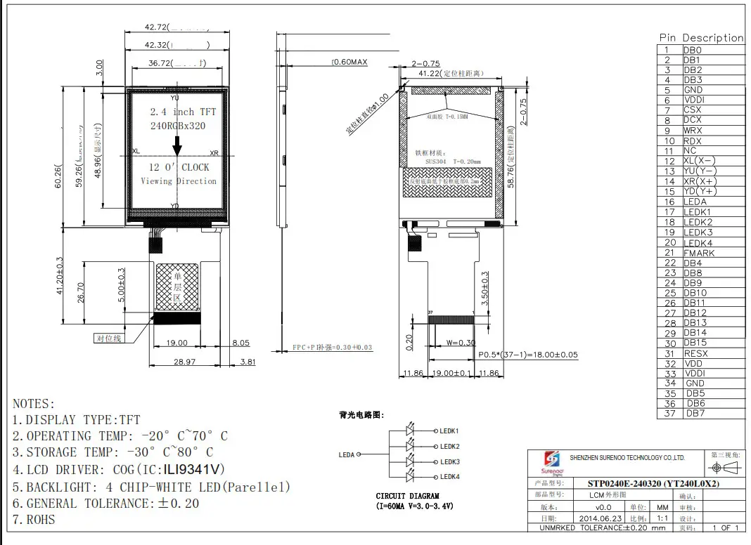
Mechanical Specification
| Item | Specifications | Unit |
| Dimensional outline | 42.72(W)*60.26(H)*2.55(T)(NTP) 42.72(W)*60.26(H)*3.75(T)(RTP) (FPC not include) | mm |
| Resolution | 240RGB*320 | dots |
| LCD Active area | 36.72(W)*48.96 (H) | mm |
| Pixel size | 0.153(W)*0.153(H) | mm |
Mechanical Dimension
Electrical Maximum Ratings
| Item | Symbol | Min | Max | Unit | Note |
| Supply voltage(VDDI) | V | 1.8 | 3.3 | V | – |
| Supply voltage(VDD) | V | 2.8 | 3.3 | V | – |
| Operating temperature | TOPR | -20 | 70 | ℃ | – |
| Storage temperature | TSTR | -30 | 80 | ℃ | – |
Brightness characteristic&Power dissipation
| Item | Symbol | Min | Typical | Max | Unit |
| LED module Forward voltage LED | VLED | 2.9 | 3.1 | 3.3 | V |
| LED module current LED | ILED | – | 60 | – | mA |
| LCD Surface Luminance | LS | 550 | 600 | – | Cd/m2 |
| LCM Surface brightness uniform LED | LD | 80 | – | – | % |
| LCD power dissipation | PLCD | – | 0.22 | – | W |
Module Function Description
| PIN No. | Symbol | Description | Notes |
| 1-4 | DB0-DB3 | MCU parallel interface data bus. | – |
| 5 | GND | Ground | – |
| 6 | VDDI | Power Supply for I/O System. | – |
| 7 | CSX | -Chip selection pin Low enable. High disable. |
– |
| 8 | DCX | -Display data/command selection pin in parallel interface. DCX=’1’: display data or parameter. |
– |
| 9 | WRX | -Write enable in MCU parallel interface. | – |
| 10 | RDX | -Read enable in 8080 MCU parallel interface. -If not used, please fix this pin at VDDI or GND. ( | – |
| 11 | NC | No connection | – |
| 12 | XL(X-) | Touch panel Logical foot | – |
| 13 | YU(Y-) | Touch panel Logical foot | – |
| 14 | XR(X+) | Touch panel Logical foot | – |
| 15 | YD(Y+) | Touch panel Logical foot | – |
| 16 | LEDA | Anode of Backlight (2.9V-3.3V Typical:3.1V) | – |
| 17 | LEDK1 | Cathode of Backlight | – |
| 18 | LEDK2 | Cathode of Backlight | – |
| 19 | LEDK3 | Cathode of Backlight | – |
| 20 | LEDK4 | Cathode of Backlight | – |
| 21 | FMRAK | Tearing effect signal is used to synchronize MCU to frame memory | – |
| 22 | DB4 | MCU parallel interface data bus. | – |
| 23-30 | DB8-DB15 | MCU parallel interface data bus. | – |
| 31 | RESX | -This signal will reset the device and it must be applied to properly initialize the chip. -Signal is active low. | – |
| 32 | VDD | Power Supply for Analog, Digital System and Booster Circuit. 2.8-3.3V) | – |
| 33 | VDDI | Power Supply for I/O System. (I/O 1.8-3.3V) | – |
| 34 | GND | Ground | – |
| 35-37 | DB5-DB7 | MCU parallel interface data bus. | – |
6-1: 6.2:
6.2: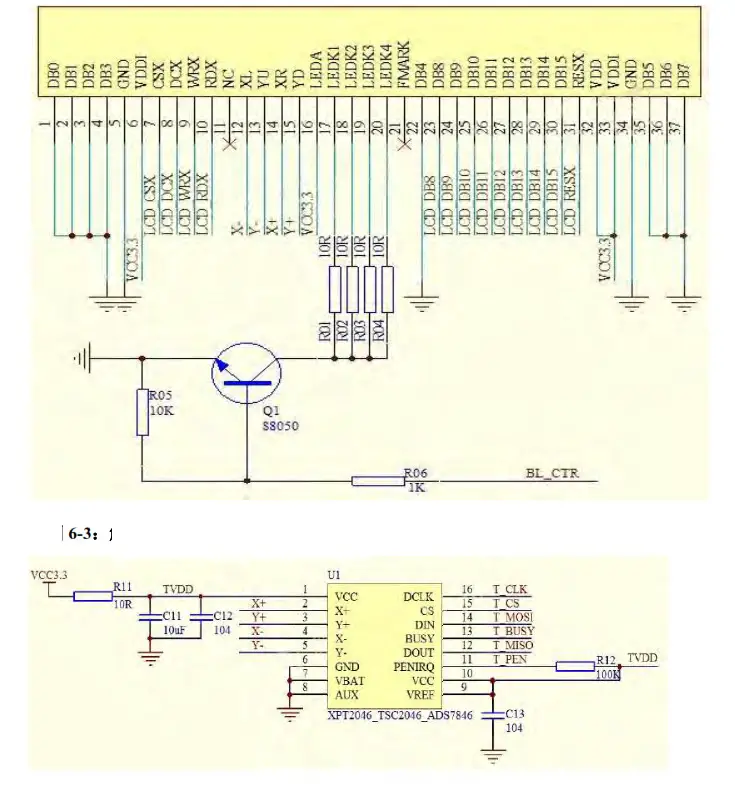
※NOTE:
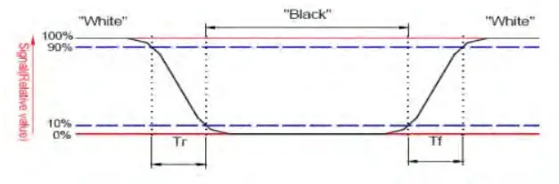
Response time&Contrast ratio
| Item | Symbol | Condition | Remark | Unit | ||
| Min. | Typ. | Max. | ||||
| Response time | Tr+Tf | θ=0° | – | 25 | 40 | ms |
| Contrast ratio | CR | θ=0° | 350 | 500 | – | – |
Viewing Angle
| Item | Symbol | Condition | Remark | Unit | ||
| Min. | Typ. | Max. | ||||
|
Viewing angle | Top 12 | CR≥10 | 40 | 50 | – |
Deg. |
| Bottom 6 | CR≥10 | 55 | 65 | – | ||
| Left 9 | CR≥10 | 55 | 65 | – | ||
| Right 3 | CR≥10 | 55 | 65 | – | ||
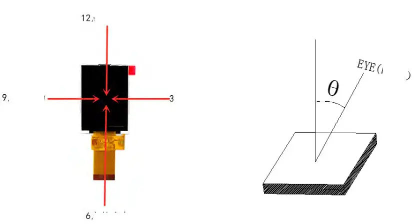
NOTE:3
Reliability Trial
| NO. | ITEM | CONDITION | CRITERION |
| 1 | High Temperature Non-Operating Test | 80℃*120Hrs | No Defect Of |
| Operational | |||
| 2 | Low Temperature Non-Operating Test | -30℃*120Hrs | Function In Room |
| Temperature Are | |||
| 3 | High Temperature/Humidity Non Operating Test | 60℃*90%RH*120Hrs | Allowable |
| 4 | High Temperature Operating Test | 70℃*72Hrs | |
| 5 | Low Temperature Operating Test | -20℃*72Hrs | |
| 6 | Thermal Shock Test | -20 ℃ (30Min) n 70 ℃ | |
| (30Min) *10CYCLES |
Inspection standards
10.1Glass defect
| NO | Defect item | Criteria | Remark |
| 1 | Dimension Unconformity (Major defect) | By Engineering Drawing | |
|
2 | Cracks (Major defect) | 1. Linear cracks panel 【Reject】 2. Nonlinear crack contrast by limited sample | 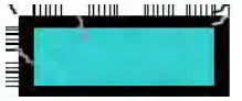 |
|
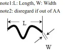
3 | Glass extrude the conductive area (minor defect) | a: disregards and no influence assemblage. 1) b≤1/3Pin width(non bonding area) 【Accept】 2)bonding area≤0.5mm 【Accept】 | A: Length, b: Width |
|
4 | Pin-side ,conductive area damaged (minor defect) | (a c: disregards) b≤1/3of effective length for bonding electrode 【Accept】 |  |
| 5 | Pin-side,non-conductive area damaged | 1)Damage area don’t touch the ITO (Inclueling contraposition mark, | a: Length, b: Width c: Thickness |
| (minor defect) | except scribing mark) 【Accept】 2) C<T b≦BM1/3of width 【Accept】 3) c=T b not touch the seal glue 【Accept】 4) a disregards |
| |
|
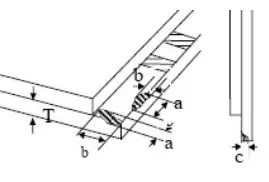
6 | Non-pin-side damage (minor defect) | c<T 1)b exceeds 1/3Bm 【Reject】 c=T b not touch the seal glue 【Reject】 | 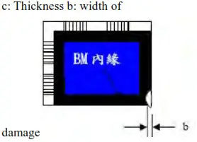 |
10.2LCD appearance defect(View area)
| NO | Defect item | Criteria | Remark | |
|
1 |
Fiber、glass cratch、polarizer scratch/folded (minor defect) | Specification | Allowable |
|
| W≦0.03mm | disregard | |||
| 0.03mm<W≦0.05mm; L≦3.0mm | 2 | |||
| 0.05mm<W≦0.1mm; L≦3.0mm | 1 | |||
| W>0.1mm;L>3.0mm | 0 | |||
|
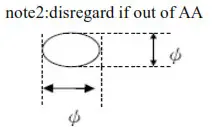
2 | Polarizer bubble、concave and convex (minor defect) | φ≦0.2mm | disregard | note1: φ=(L+W)/2,L:Length, W :Width note2:disregard if out of AA |
| 0.2mm<φ≦0.3mm | 2 | |||
| 0.3mm<φ≦0.5mm | 1 | |||
| 0.5mm<φ | 0 | |||
|
3 | Black dots、dirty dots、impurities、eye winker (minor defect) | φ≦0.15mm | disregard |
|
| 0.15mm<φ≦0.25mm | 2 | |||
| 0.25mm<φ≦0.3mm | 1 | |||
| 0.3mm<φ | 0 | |||
|
4 | Polarizer prick (minor defect) | φ≦0.1mm | disregard | note1: φ=(L+W)/2,L=Length, W=Width note2:the distance between two dots>5mm |
| 0.1mm<φ≦0.25mm | 3 | |||
| φ>0.25mm | 0 | |||
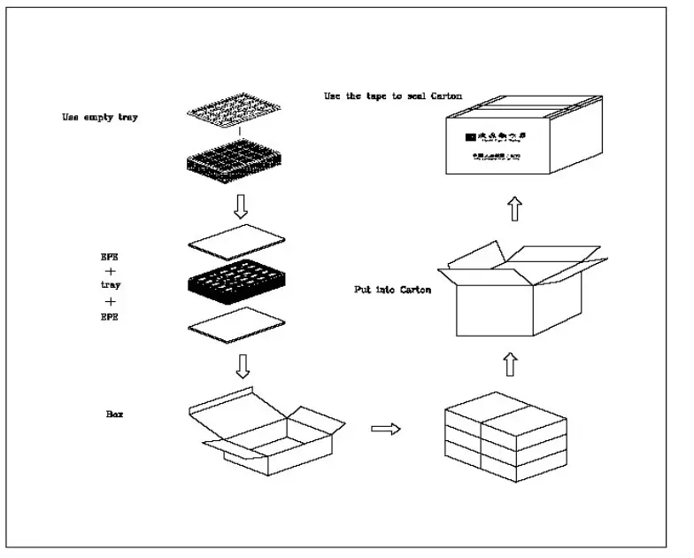
Package Method
 .
.
 |  |  |  |
| https://wa.me/qr/4GGOIDYZ2PXXN1 | http://qr.kakao.com/talk/THom9tzJN5OMzvx1vTL1V.LvnEc- | https://line.me/ti/p/oas8BmVLVd | https://u.wechat.com/EAK0B_l2YfPLwx3tRqiKkf4 |
https://line.me/ti/p/oas8BmVLVd
www.surenoo.com
Shenzhen Surenoo Technology Co.,Ltd.
www.surenoo.com
Skype: Surenoo365


