Surenoo STP0154D-240240 Series TFT LCD Panel User Manual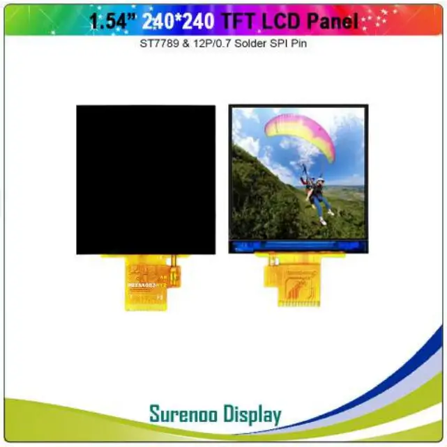
Revised History
| Part Number | Revision | Revision Content | Revised on |
| STP0154D-240240 | A N | ew | 2021-04-23 |
General Description
Description
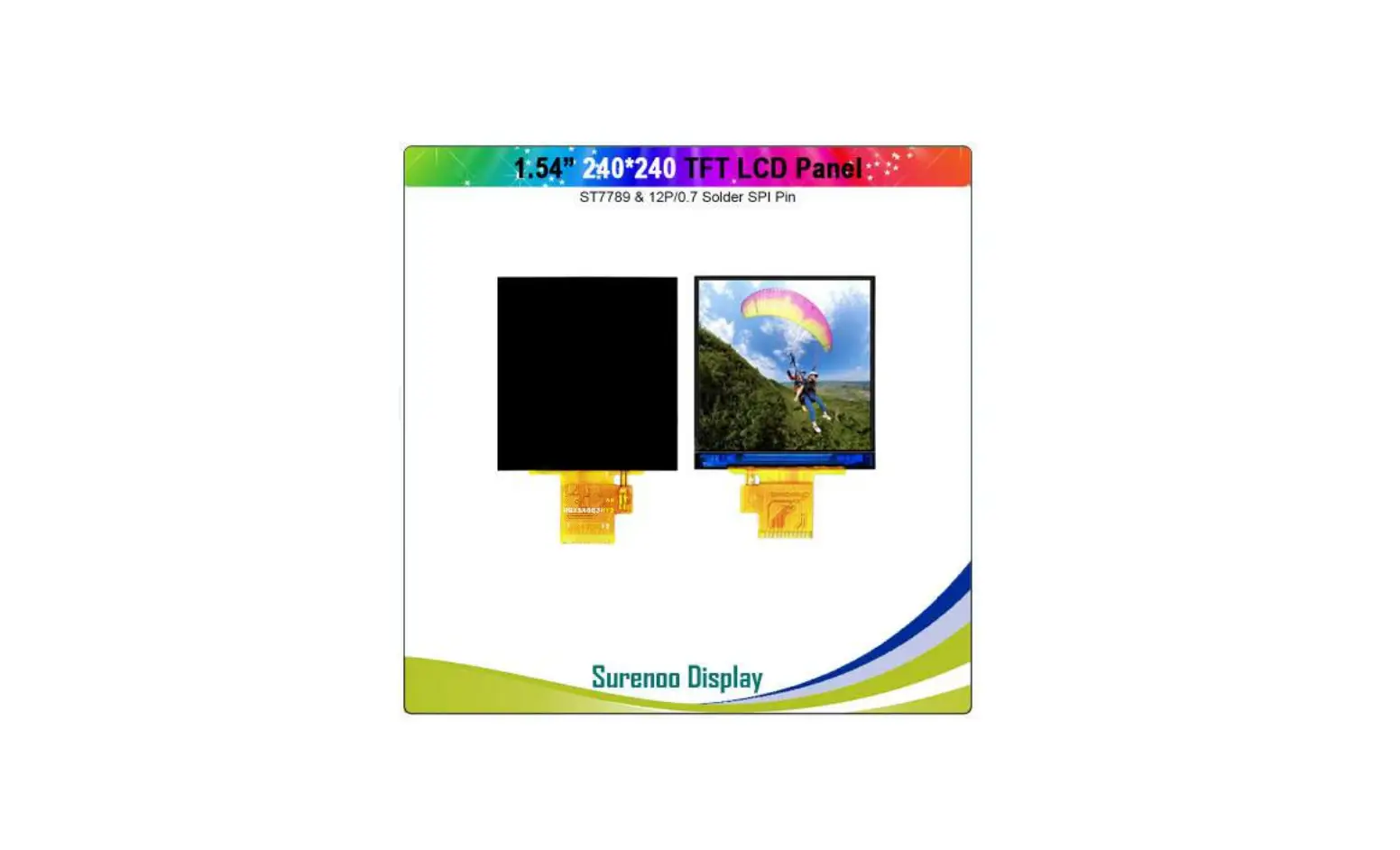
STP0154D-240240 is a 240RGBX240 dot-matrix TFT LCD module. This module is composed of a TFT LCD Panel, driver ICs, FPC and a Backlight unit.
Features
| NO. | Item | Contents | Unit |
| 1 | LCD Size | 1.54 | inch |
| 2 | Display Mode | Normally black | – |
| 3 | Resolution | 240(H)RGB x240(V) | pixels |
| 4 | Pixel pitch | 0.1155(H) x 0.1155(V) | mm |
| 5 | Active area | 27.72(H) x 27.72(V) | mm |
| 6 | Module size | 31.52(H) x 33.72(V) x1.9 (D) | mm |
| 7 | Pixel arrangement | RGB Vertical stripe | – |
| 8 | Interface | 4 Line SPI | – |
| 9 | Display Colors | 262K | colors |
| 10 | Drive IC | ST7789V3 | – |
| 11 | Luminance(cd/m2) | 400 (TYP) | Cd/m2 |
| 12 | Viewing Direction | All View | Best image |
| 13 | Backlight | 3 White LED Parallel | – |
| 14 | Operating Temp. | -20℃~ + 70℃ | ℃ |
| 15 | Storage Temp. | -30℃~+ 80℃ | ℃ |
| 16 | Weight | 2.8 | g |
Mechanical Drawing
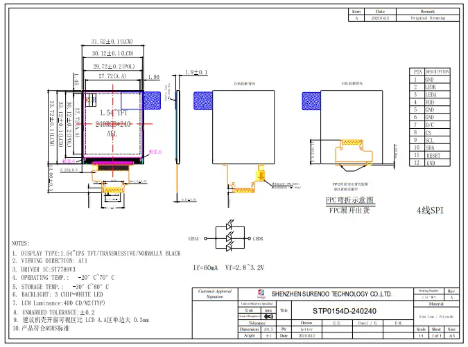
Pin Definition
FPC Connector is used for the module electronics interface.
| NO. | Symbol | Description |
| 1 | GND | Power Ground |
| 2 | LEDK | LED Cathode |
| 3 | LEDA | LED Anode |
| 4 | VDD | Power Supply for Analog |
| 5 | GND | Power Ground |
| 6 | GND | Power Ground |
| 7 | D/C | Display data/command selection pin in 4-line serial interface. |
| 8 | CS | Chip selection pin ;Low enable ,high disable. |
| 9 | SCL | This pin is used to be serial interface clock |
| 10 | SDA | SPI interface input/output pin .the data is latched on the rising edge of the SCL signal. |
| 11 | RESET | This signal will reset the device and it must be applied to properly initialize the chip .Signal is active low. |
| 12 | GND | Power Ground |
Note: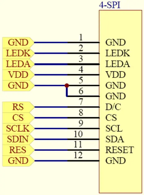
Electrical Characteristics
Absolute Maximum Ratings
| Parameter | Symbol | Min | MAX | Unit | Notes |
| Supply Voltage (I/O) | VDD | -0.3 | 4.6 | V | |
| Analog Supply Voltage | VDDIO | -0.3 | 4.6 | V | |
| Logic Input Voltage | VIN | -0.3 | VDDIO+0.5 | V | |
| Operation Temperature | Top | -20 | 70 | ℃ | |
| Storage Temperature | Tst | -30 | 80 | ℃ |
Operating Conditions
| Parameter | Symbol | Min | TYP | MAX | Unit | Notes |
| System Voltage | VDD | 2.5 | 2.8 | 3.3 | V | |
| Gate Driver High Voltage | VGH | 12.2 | – | 14.97 | V | |
| Gate Driver Low Voltage | VGL | -12.5 | – | -7.16 | V | |
| Operating Current for VDD | IDD | – | 8 | 10 | mA | |
| Sleep_In Mode VDD | I dd | – | 15 | 30 | uA | |
| Sleep_In Mode VDDIO | I ddio | – | 5 | 10 | uA |
Backlight Unit
| Parameter | Symbol | Min | TYP | MAX | Unit | Notes |
| Voltage for LED backlight | VLED | 2.8 | 3.0 | 3.2 | V | |
| Current for LED backlight | ILED | – | 60 | 90 | mA | 3 LED |
| Power Consumption | Pbl | – | 180 | 288 | mW | 1 |
| Brightness | Lbr | 350 | 400 | – | cd/m2 | 2 |
| LED Life time | – | 20000 | – | – | hr | 3 |
Note:
- Where ILED =60mA , VLED=3.0V , Pbl= ILED x VLED
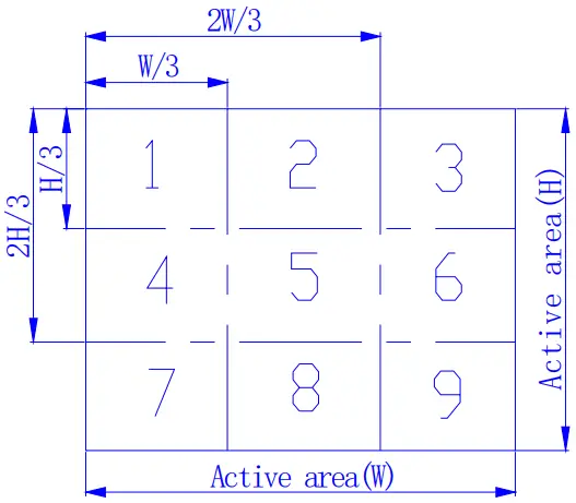
- Uniform measure condition:
- Measure 9 point ,Measure location is show below:
- Uniform=(Min brightness/Max brightness)x100%
- Best Contrast.
- The environmental conducted under ambient air flow ,at Ta=25±2o C,60%RH±5%
Backlight Recommended Circuit
Motherboard driver backlight is need constant current circuit , if threated voltage screen after light brightness difference . Current and power consumption of the machine are inconsistent , so recommend a backlight driving circuit is best rated current . It is recommended to use IC (AW9364) . The reference circuit is as follows: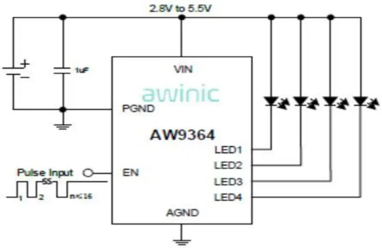
AC Timing Characteristic of The LCD
Serial interface Characteristics(4-line serial):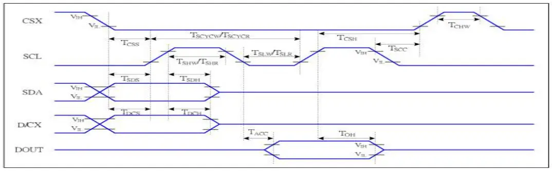
| ISignal | Symbol | , Parameter | MIN | MAX | Unit | Description |
| CSX | Tcss | Chip select setup time (write) | 15 | ns | ||
| Tcst-, | Chip select hold time (write) | 15 | ns | |||
| Tcss | Chip select setup time (read) | 60 | ns | |||
| Tscc | Chip select hold time (read) | 65 | ns | |||
| Tar* | Chip select “H” pulse width | 40 | ns | |||
| SCL | Tscycw | Serial clock cycle (Write) | 16 | ns | -write command & data ram | |
| TsHw | SCL “H” pulse width (Write) | 7 | ns | |||
| Taw | SCL “L” pulse width (Write) | 7 | ns | |||
| TSCYCR | Serial clock cycle (Read) | 150 | ns | -read command & data ram | ||
| TSHR | SCL “H” pulse width (Read) | 60 | ns | |||
| TSLR | SCL “L” pulse width (Read) | 60 | ns | |||
| D/CX | Tocs | D/CX setup time | 10 | ns | ||
| TECH | D/CX hold time | 10 | ns | |||
| SDA (DIN) | Tsns | Data setup time | 7 | ns | ||
| TSCH | Data hold time | 7 | ns | |||
| DOUT | TACC | Access time | 10 | 50 | ns | For maximum CL=3OpF For minimum CL.8pF |
| TOH _ | Output disable time | 15 | 50 | ns |
OPTICAL CHARACTERISTICS
| Item | Symbol | Measuring Conditions | Min. | Typ. | Max. | Unit | Remark | |
| Viewing Angle | q | f = 0o | 25 oC | 70 | 80 | – | Deg | Note1 |
| f =180o | 25 oC | 70 | 80 | – | ||||
| q | f = 90o | 25 oC | 70 | 80 | – | |||
| f =270o | 25 oC | 70 | 80 | – | ||||
| Brightness | Lbr | — | – | 350 | 400 | – | Cd/m2 | |
| Luminance Uniformity | ∆L | — | – | 70 | 75 | – | ||
| Contrast Ratio | CR | — | 25 oC | 700 | 900 | – | — | Note2 |
| Response Time | Tr +Tf | q = 0o f = 0o | 25 oC | – | 30 | 40 | ms | Note3 |
| Color of CIE Coordinate | White | X | 25 oC |
-0.03 | 0.320 | +0.03 | — | BM-7A |
| Y | 25 oC | 0.343 | ||||||
| Red | X | 25 oC | 0.612 | |||||
| Y | 25 oC | 0.327 | ||||||
| Green | X | 25 oC | 0.334 | |||||
| Y | 25 oC | 0.536 | ||||||
| Blue | X | 25 oC | 0.137 | |||||
| Y | 25 oC | 0.150 | ||||||
| Transmittance (with polarizer) | — | — | — | 4.4 | 4.9 | – | % | — |
Note 1 Definition of Viewing Angle: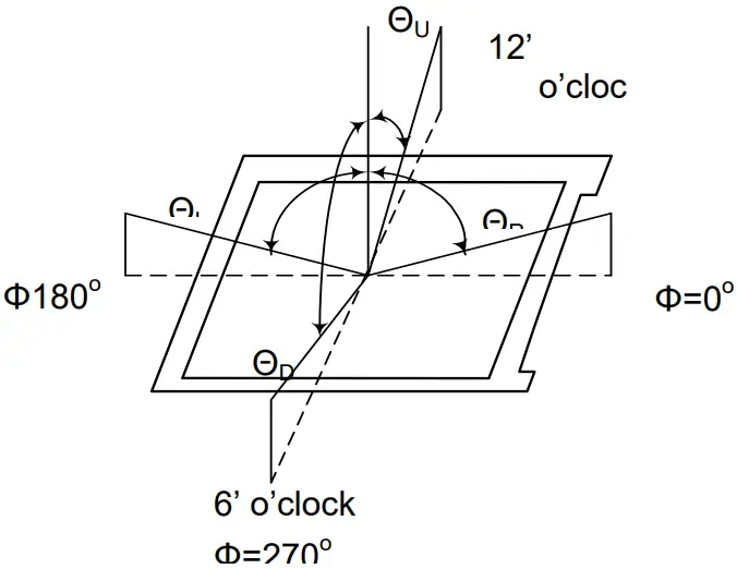
Note 2:Definition of Contrast Ratio (CR) : measured at the center point of panel
CR =
Luminance with all pixels white
Luminance with all pixels black
Note 3: Definition of Response Time : Sum of Tr and Tf :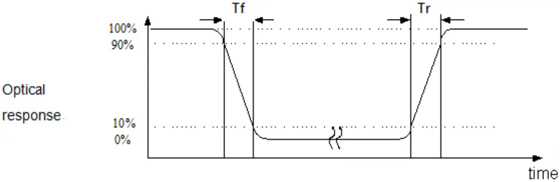
Reliability
Contents of Reliability Tests
| No. | Item | Conditions | Note |
| 1 | High Temperature Operation | 70°C±2°C, 120 hrs | |
| 2 | Low Temperature Operation | -20°C±2°C, 120 hrs | |
| 3 | High Temperature Storage | 80°C±2°C, 120 hrs | |
| 4 | Low Temperature Storage | -30°C±2°C, 120 hrs | |
| 5 | High Temperature /Humidity Operation | 60°C±2°C, 90% RH, 120 hrs | |
| 6 | Temperature Cycling | -10°C→25°C→60°C→25°C→-10°C 30min 5min 30min 5min 30min 10 cycle. | |
| 7 | Vibration Test | Total fixed amplitude:1.5mm. Vibration Frequerncy:10~55Hz One cycle 60 seconds to 3 direction of X,Y,Z each 15 minutes. | |
| 8 | ESD Test | Air Discharge: Apple ±4KV with 5 times. | |
| Contact Discharge: Apple ±2KV with 5 times. | |||
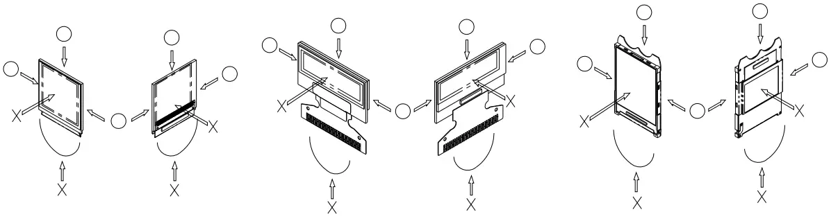
| 9 | Drop Test | 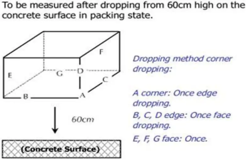 |
Note:
No charge on display and in operation under the following test condition.
Please note that the reliability test project requires the use of virgin samples
Condition : Unless otherwise specified ,tests will be conducted under the following condition.
Temperature: 20C±5C.
Humidity: 65±5%RH.
Tests will be not conducted under functioning state.
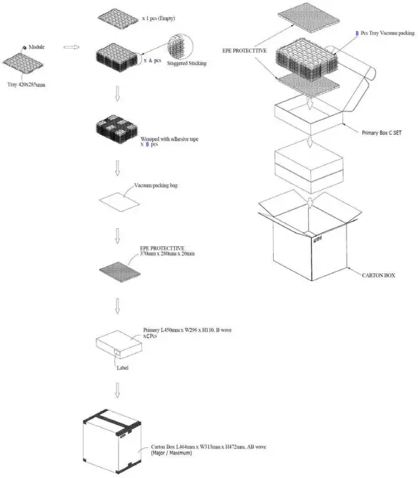
Package Specifications
| Item | Quantity | ||
| Module | 720 | per Primary Box | |
| Holding Trays | (A) | 15 | per Primary Box |
| Total Trays | (B) | 16 | per Primary Box (Including 1 Empty Tray) |
| Primary Box | (C) | 1~4 | per Carton (4 as Major / Maximum) |
Incoming Inspection Standards
Inspection and Environment Conditions
Inspection Conditions:
- Inspection Distance :35 cm±5cm
- View Angle : Light-on Inspection Angle: ±5°
Cosmetic Inspection Angle: ±45°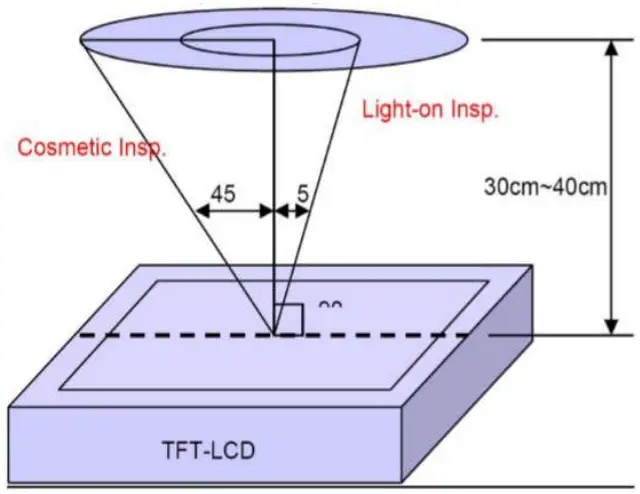
Environment Conditions:
| Ambient Temperature | 23℃±5℃ | |
| Ambient Humidity | 55±10%RH | |
| Ambient Illumination | Cosmetic Inspection Functional Inspection | More than 600 Lux 300~500 Lux |
Sampling Conditions:
- Lot Size: Quantity of shipment lot per model
- Sampling Method:
| Sampling Plan | MIL-STD-105E | |
| Normal Inspection Single Sampling | ||
| Level II | ||
| AQL | Major Defect Minor Defect | 0.65% 1.5% |
Inspection Criteria
Cosmetic Inspection(Panel):
| Check Item | Classification | Criteria(Unit: mm) |
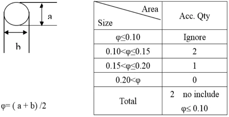
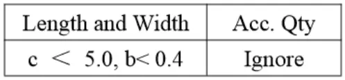
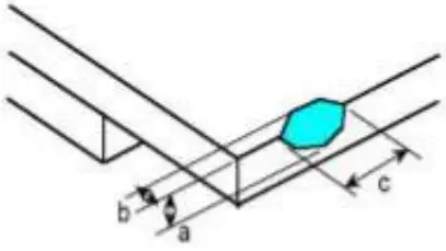
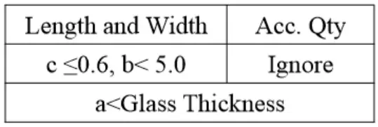
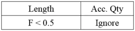
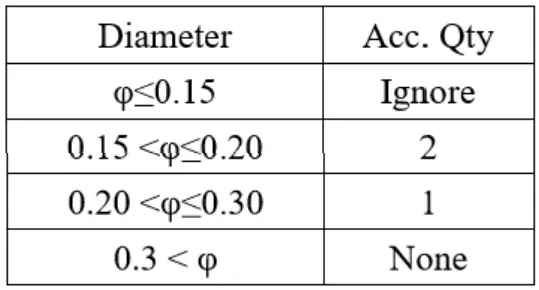
| Black / White spot Foreign material (Round type) Pinholes Stain Particles inside cell. | Minor |
|
| Distance between 2 defects should more than 5mm apart. | ||
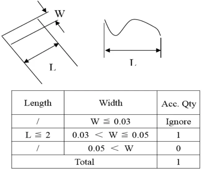
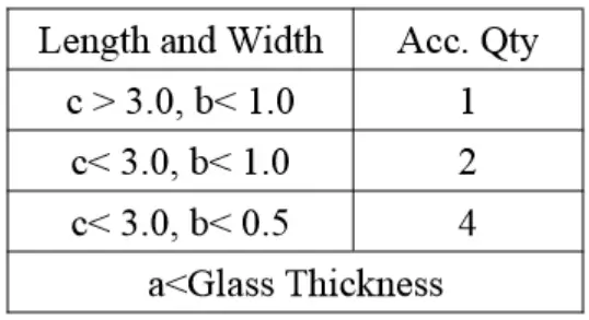
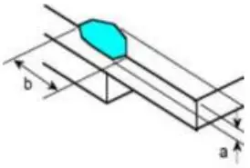
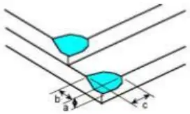
| Black and White line Scratch Foreign material (Line type) | Minor |
|
| Distance between 2 defects should more than 5mm apart. | ||
| Scratches not viewable through the back of the display are | ||
| acceptable.
| ||
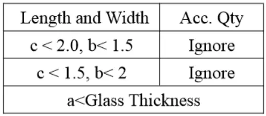
| Glass Crack | Minor |
|
| LCD with extensible crack line is unacceptable(When press the | ||
| cracked LCD Area, the line will expand, we define it is extensible | ||
| crack line) | ||
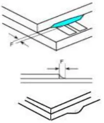
| Glass Chipping Pad | ||
| Area | ||
 | Minor |
|
| Check Item | Classification | Criferia(Unit: mm) |
Glass Chipping Rear Of Pad Area | Minor |
|
I Glass Chipping Except Pad Area | Minor |
|
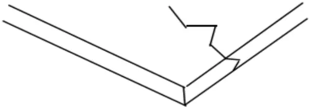
Glass Corner Chipping | Minor |
|
Glass BUTT | Minor | Glass burr don’t affect assemble and module dimension. |
FPC Defect | Minor |
|
| Bubble on Polarizer | Minor |
|
| Check Item | Classification | Criteria(Unit: mm) |
| Dent on Polarizer | Minor |
|
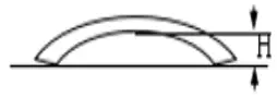
Screen deformation | / | Test for insertion of plug gauge at highest warping point: H._:: 0.25mm The client has special requirements, according to drawing. |
| Bezel | / |
|
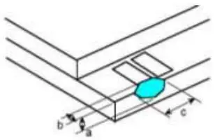
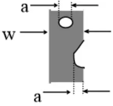
| Touch Panel | / | D. Diameter W: width L: length
|
| PCB | / |
|
| Soldering | / | Follow IPC-A-610C standard. |
| Leak | / | Yellow light. OK_ White light. According to the limit sample |
| Check Item | Classification | Criteria(Unit: mm) |
| Electrical Defect | Major | The below defects must be rejected.
|
Precautions When Using These TFT Display Modules
Handling Precautions
- Since the display panel is being made of glass, do not apply mechanical impacts such us dropping from a high position.
- If the display panel is broken by some accident and the internal organic substance leaks out, be careful not to inhale nor lick the organic substance.
- If pressure is applied to the display surface or its neighborhood of the TFT display module, the cell structure may be damaged and be careful not to apply pressure to these sections.
- The polarizer covering the surface of the TFT display module is soft and easily scratched. Please be careful when handling the TFT display module.
- When the surface of the polarizer of the TFT display module has soil, clean the surface. It takes advantage of by using following adhesion tape.
Scotch Mending Tape No. 810 or an equivalent
Never try to breathe upon the soiled surface nor wipe the surface using cloth containing solvent such as ethyl alcohol, since the surface of the polarizer will become cloudy.
Also, pay attention that the following liquid and solvent may spoil the polarizer:- Water
- Ketone
- Aromatic Solvents
- Hold TFT display module very carefully when placing TFT display module into the system housing. Do not apply excessive stress or pressure to TFT display module. And, do not over bend the film with electrode pattern layouts. These stresses will influence the display performance. Also, secure sufficient rigidity for the outer cases.
- Do not apply stress to the driver IC and the surrounding molded sections.
- Do not disassemble nor modify the TFT display module.
- Do not apply input signals while the logic power is off.
- Pay sufficient attention to the working environments when handing TFT display modules to prevent occurrence of element breakage accidents by static electricity.
- Be sure to make human body grounding when handling TFT display modules.
- Be sure to ground tools to use or assembly such as soldering irons.
- To suppress generation of static electricity, avoid carrying out assembly work under dry environments.
- Protective film is being applied to the surface of the display panel of the TFT display module.
Be careful since static electricity may be generated when exfoliating the protective film.
- Protection film is being applied to the surface of the display panel and removes the protection film before assembling it. At this time, if the TFT display module has been stored for a long period of time, residue adhesive material of the protection film may remain on the surface of the display panel after removed of the film. In such case, remove the residue material by the method introduced in the above Section 5).
- If electric current is applied when the TFT display module is being dewed or when it is placed under high humidity environments, the electrodes may be corroded and be careful to avoid the
above.
Storage Precautions
- When storing TFT display modules, put them in static electricity preventive bags avoiding
exposure to direct sun light nor to lights of fluorescent lamps. and, also, avoiding high temperature and high humidity environment or low temperature (less than 0C) environments. (We recommend you to store these modules in the packaged state when they were shipped from
Limit to technology Inc.) y At that time, be careful not to let water drops adhere to the packages or bags nor let dewing occur with them. - If electric current is applied when water drops are adhering to the surface of the TFT display module, when the TFT display module is being dewed or when it is placed under high humidity environments, the electrodes may be corroded and be careful about the above.
Designing Precautions
- The absolute maximum ratings are the ratings which cannot be exceeded for TFT display module, and if these values are exceeded, panel damage may be happen.
- To prevent occurrence of malfunctioning by noise, pay attention to satisfy the VIL and VIH specifications and, at the same time, to make the signal line cable as short as possible.
- We recommend you to install excess current preventive unit (fuses, etc.) to the power circuit (VDD). (Recommend value: 0.5A)
- Pay sufficient attention to avoid occurrence of mutual noise interference with the neighboring devices.
- As for EMI, take necessary measures on the equipment side basically.
- When fastening the TFT display module, fasten the external plastic housing section.
- If power supply to the TFT display module is forcibly shut down by such errors as taking out the main battery while the TFT display panel is in operation, we cannot guarantee the quality of this OEL display module.
- The electric potential to be connected to the rear face of the IC chip should be as follows:
- Connection (contact) to any other potential than the above may lead to rupture of the IC.
Precautions when disposing of the TFT display modules
- Request the qualified companies to handle industrial wastes when disposing of the TFT display modules. Or, when burning them, be sure to observe the environmental and hygienic laws and regulations.
Other Precautions
- When an TFT display module is operated for a long of time with fixed pattern may remain as an after image or slight contrast deviation may occur.
Nonetheless, if the operation is interrupted and left unused for a while, normal state can be restored. Also, there will be no problem in the reliability of the module. - To protect TFT display modules from performance drops by static electricity rapture, etc., do not touch the following sections whenever possible while handling the TFT display modules.
- Pins and electrodes
- Pattern layouts such as the FPC
- With this TFT display module, the TFT driver is being exposed. Generally speaking, semiconductor elements change their characteristics when light is radiated according to the
principle of the solar battery. Consequently, if this TFT driver is exposed to light, malfunctioning
may occur.- Design the product and installation method so that the TFT driver may be shielded from light in actual usage.
- Design the product and installation method so that the TFT driver may be shielded from light during the inspection processes.
- Although this TFT display module stores the operation state data by the commands and the indication data, when excessive external noise, etc. enters into the module, the internal status may be changed. It therefore is necessary to take appropriate measures to suppress noise generation or to protect from influences of noise on the system design.
- We recommend you to construct its software to make periodical refreshment of the operation statuses (re-setting of the commands and re-transference of the display data) to cope with catastrophic noise.
Warranty
The warranty period shall last twelve (12) months from the date of delivery. Buyer shall be completed to assemble all the processes within the effective twelve (12) months. technology Inc. shall be liable for replacing any products which contain defective material or process which do not conform to the product specification, applicable drawings and specifications during the warranty period. All products must be preserved, handled and appearance to permit efficient handling during warranty period. The warranty coverage would be exclusive while the returned goods are out of the terms above.


 Series Tft Lcd Panel User Manual")


