 VICOR PI352X-0X-EVAL1 ZVS Regulators 60VIN Buck Evaluation Board
Introduction
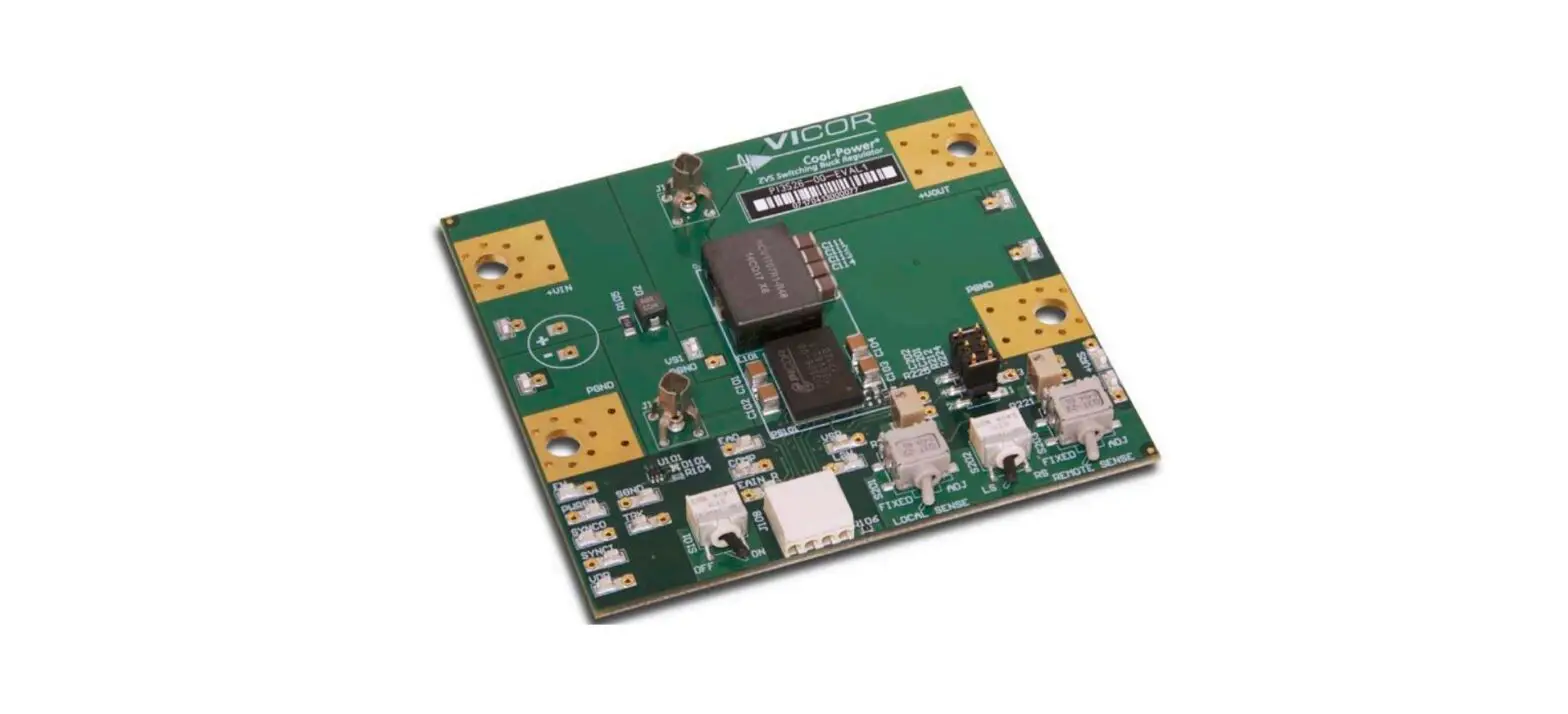
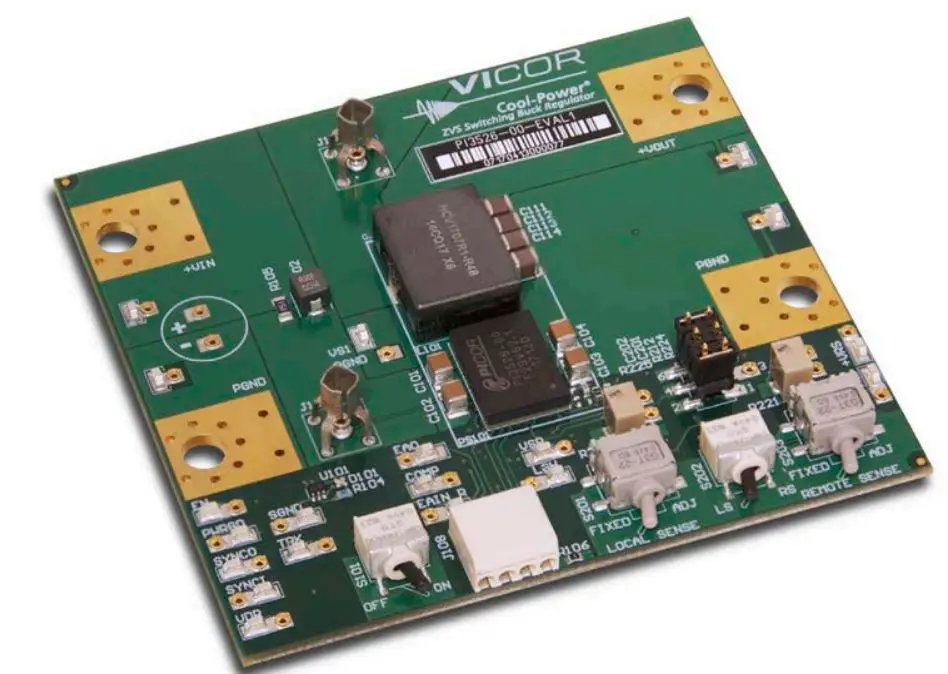
This evaluation board is designed for the PI352x family of 10 x 14 ZVS Bucks. It can be configured to demonstrate a single product in a stand-alone local sense or a remote sense configuration.
The PI352x family of wide input range DC-DC ZVS-Buck regulators feature high efficiency with integrated controller, power switches, and support components all within a high density 0.4” x 0.55” System-in-Package (SiP). Required components are placed inside a demarcation featuring a solution size of 7.3” x 1.35”. The demarcation includes an external inductor, compensation capacitor, voltage selection resistors, soft-start capacitor, and input-output capacitors to form a complete DC-DC regulator.
IMPORTANT NOTICE: Be sure to read the precautions below entirely BEFORE using the Evaluation Board. Do not operate the evaluation board unless you have the appropriate safety precautions in place on your bench to ensure a successful experience. The list below is not comprehensive and is not a substitute for common sense and good practice.
- Refer to the specific regulator module datasheet for an electrical rating of the device, and thermal and mechanical product details. It is important to remain within the device-rated range when testing.
- When testing electronic products always use approved safety glasses. Follow good laboratory practices and procedures.
- During operation insure the power devices and surrounding structures can be operated safely.
- Care should be taken to protect the user from accidental contact when under power.
- Provide a strain relief for wires and place the system on the bench in such a way as to prevent accidental displacement from the benchtop.
- Review thermal considerations and guidelines associated with operating the evaluation board. Most notably use a benchtop fan and use rubber feet to elevate the PCB as they allow airflow to
the bottom. - Remove power and use caution when connecting and disconnecting test probes and interface lines to avoid inadvertent short circuits and contact with hot surfaces.
- Verify power connections to avoid reversing applied voltage polarities.
- Avoid creating ground loops between the SGND and PGND pins when making measurements.
- The product evaluation board is designed for general laboratory evaluation. It is not recommended for installation in end-user equipment.
- The evaluation board is designed to facilitate the evaluation of the performance of Vicor’s mounted ZVS buck products. Sockets are provided to permit quick probing. Input sockets can be used to place a bulk capacitor. The evaluation board provides lugs, and bottom layer banana jack footprint for input and output connections, signal connectors allowing wire, signal test points for easy connection to standard test equipment, and Kelvin Johnson-Jack for accurate voltage measurements of power nodes.
Box Contents
The evaluation board ships with the following contents:
- 1 Customer evaluation board
- 3 x pre-installed jumpers
- 1 x hardware kit: 5 x size 10 screws, lugs and washers
Recommended Test Equipment
The following is a list of recommended test equipment.
- Safety glasses.
- DC power supply: Refer to the specific PI352x model datasheet to ensure the supply has sufficient power and current capability.
- Electronic load: Refer to the specific PI352x model datasheet to ensure the load has sufficient power handling and current capability for testing.
- Bench top cooling fan.
- Digital multi-meters (DMMs).
- Oscilloscope and probes.
- Interconnect wires, cables and fastening hardware.
Features
- Input and output lugs for source and load connections.
- Input sockets to place through-hole input aluminum-electrolytic capacitor.
- Input source filter (L102, R105).
- Toggle switch (S101) for enabling and disabling the regulator through the EN pin.
- Oscilloscope probe jack for accurate, high frequency input (J101) and output (J102) voltage measurement.
- Signal pins test points and wire connectors.
- Kelvin voltage test points and sockets for all pins of the SiP product.
- Access to voltage switching node VS1 with a nearby ground receptacle.
- Mode selection switch for local (default) and remote sense loop.
- Trim control selection for both local and remote sense:
- ADJ: potentiometer to exercise the full output range.
- Fixed: resistor to set unit to nominal output.
- Local and remote sense AC signal injection (J201).
Board Operation Modes
- S101 provides control to enable / disable the powertrain.
- In the “OFF” position, the switch will connect SGND pin to the EN net, which disables the regulator output.
- In the “ON” position, the EN net is allowed to float.
- The PI352x evaluation board supports the following operating modes:
| Mode | S202 | S201 | S203 | J201 | (+VRS, -VRS) |
| Local loop, fixed Nominal output | LS | FIXED | – | Place jumper (J201 pin 1-2) to short R211 for accurate result | – |
| Local loop, with Trim range (R206) |
LS |
ADJ |
– | Turn (R206) counterclockwise to increase the output voltage and clockwise to decrease the output voltage. |
– |
| Remote loop, fixed Nominal output | – | FIXED | RS | Place jumper (J201 pin 1-2) to short R211 for accurate result |
Used to connect to point of load. If not connected (R223-R224 = 100Ω) will be in the loop connecting this node to local +VOUT |
| Remote loop, with Trim range (R221) |
– |
ADJ |
RS | Turn (R206) counterclockwise to increase the output voltage and clockwise to decrease the output voltage. |
Thermal Consideration
A fan blowing across the evaluation board is recommended for operation. The fan should be placed about 4 inches away from the evaluation board edge. A typical benchtop fan is recommended providing about 1000LFM. Using the supplied rubber feet is also required in order to elevate the board about 0.4 inches off a flat surface and enable airflow underneath the PCB.
Power Up Procedure
- Confirm bench equipment is powered off.
- Connect input DC power supply positive lead to +VIN input lug, then connect input power supply negative lead to PGND input lug of the evaluation board.
- Connect the +VOUT lug to the electronic load positive input, connect the PGND output lug to the electronic load negative input.
- Verify proper polarity of both input and output connections.
- Verify on-board mechanical switch (S101) desired actuator position. “ON” state allows power up upon application of input voltage. S101 default actuator position is “ON” allowing the unit to power up upon the application of an input voltage greater than VUVLO_START.
- Verify that three separate two-position jumper sockets are placed on the header (J201) shorting the following J201 pins 1 to 2, 3 to 4, 5 to 6.
- Verify desired feedback loop operation:
- On-board mechanical switch (S202) default position is “LS” short for local sense loop
- On-board mechanical switch (S201) default position is “FIXED” implying the use of the populated exact value resistors producing a regulated, device-specific, nominal output voltage.
- Place measuring equipment such as DMM, scope probes as desired
- Direct airflow from the cooling fan towards the evaluation board.
- Download the latest product datasheet from the Vicor power product page and have it on hand for reference
- Apply input voltage greater than the minimum Input under-voltage lockout start threshold (VUVLO_START).
Board Description
The following section provides a detailed description of the evaluation board features. 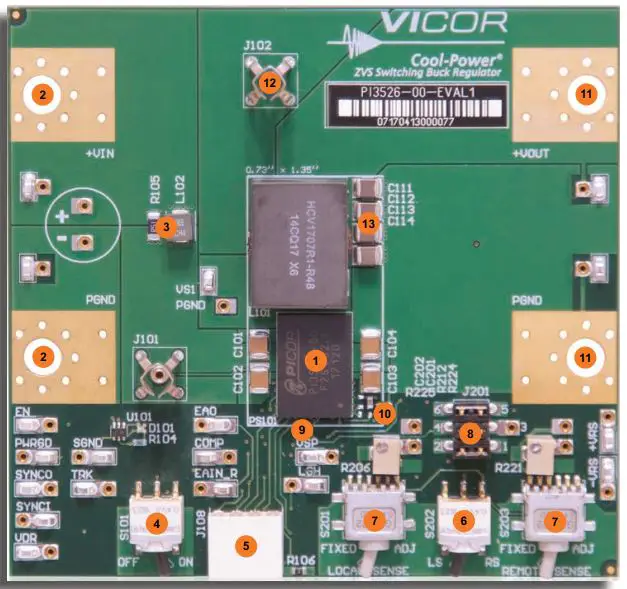
Figure 2: Signal Connector and Header Pinout, Front View 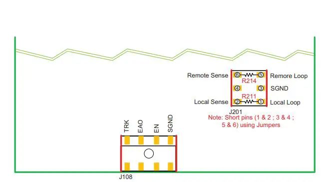
General Components
- PI352x family product (PS101)
- Input lugs: Sized for #10 hardware. Use for making connection to the input source. This board does not contain reverse polarity protection. Check for proper polarity before applying power.
- Input Filtring: Sockets provision can be used for easy installation of aluminum-electrolytic input capacitor and filtering (inductor and ceramic capacitors) allows for stable operation with most input sources. 10 x 2.2µF output ceramic capacitors 1210 (C101- C110) are used to achieve <2% of VIN peak-to-peak ripple.
- Enable / Disable switch (S101): When actuator is towards “ON” position, the (EN) pin will be open and the regulator will be allowed to power up. When actuator is towards “OFF”, the EN pin will be connected to SGND pin and the regulator will be disabled. When switch (S101) is “ON”, an external voltage source can control the EN pin state using the external EN test point.
- Wire to board connector (J108): provides access to the regulator signal. All signal pins are reference to SGND.
- TRK: An external capacitor may be connected between TRK pin and SGND to slow down the internal reference ramp. With this pin connected to an external capacitor the output voltage will track the slope effectively executing a soft-start function. See datasheet for additional tracking options.
- EAO: Internal transconductance amplifier output pin.
- EN: Regulator enable pin. Regulator is disabled when (S101) is in “OFF” state as this pin is connected to SGND. In “ON” state the module pin is allowed to float.
- SGND: Internal logic ground return for all module. SGND to PGND connection is made inside the regulator package.
- Loop compensation mode selection (S202): Used to select one of the following:
- Local Sense (LS): default. Single ended feedback loop using the internal to the regulator operational transconductance amplifier. +VOUT Lug is the local sensed location. +VOUT lug is connected to the Error Amplifier Inverting Input (EAIN) through a voltage divider network.
- Remote Sense (RS): Non-isolated remote sensing option using the internal to the regulator independent differential amplifier which outputs (VDIFF) is in turn connected to the transconductance amplifier input (EAIN) pin. Remote sensing is achieved using +VRS and –VRS test points. Resistors R223 and R224 are 100Ω catch resistor placed to prevent an open loop condition if accidentally switched to this mode.
- Trim mode selection (S201 or S203): Switch (S201) and trim potentiometer (R206) are associated with local sense loop while switch (S203) and trim potentiometer (R221) are associated with remote sense selection. Both Switches (S201 and S203) provide the following trim modes:
- Fixed Trim (FIXED): default. Fixed resistor divider is used to set regulator output to the nominal datasheet output voltage.
- Adjustable Trim (ADJ): selection allows the use of trim potentiometer (R206 or R221) to exercise the full output voltage range. Turn counterclockwise to increase the output voltage and clockwise to decrease the output voltage. The trim potentiometer at either lowest or highest point can only exercise the voltage range defined in the datasheet as valid operational range within tolerance limits. If preferred, through-hole receptacles are available to bypass the potentiometer with external leaded resistor.
- Header-jumper (J201): Default setting is all three jumper sockets populated. This header provides the following function:
- Pin 1 and pin 2 can be used to inject the isolated signal of a network analyzer through (R211= 49.9Ω) used for bode plot measurement in order to evaluate the stability in local sense mode.
- Pin 3 is SGND.
- Pin 5 and pin 6 can be used to inject the isolated signal of a network analyzer through (R214 = 49.9Ω) used for bode plot measurement in order to evaluate the stability in remote sense mode.
- Soft-start capacitor (C123): Capacitor connected to regulator TRK pin and SGND. The soft-start time is set with an internal 47nF capacitor to roughly 0.94ms. C123 can be added to further stretch the soft-start ramp CTRK = (tTRK_DESIRED x 50E-6) – 47E-9 where ITRK = 50µA.
- Internal operational transconductance amplifier compensation network (C201, R212, R225, C202): this network provides flexibility during loop compensation design to adjust the compensation. For the purpose of this evaluation board, C201 in series to the internal R(ZI) of 5kΩ is used.The maximum mid-band gain that can be achieved when using the internal R(ZI) is roughly (20•log(R(ZI)•gm•VREF/VOUT_SET). With a reference voltage of 0.99V and output voltage of 5V max mid band gain is ~14dB. R212 + R(ZI) in series can be used to further increase the mid-band gain. C202 can be used to lower the high-frequency pole if desired. The high-frequency pole is set internally to ~1.7Mhz using a C(HF) = 56pF.
- Output lugs: Sized for #10 hardware. Use these lugs to connect the output directly to the load.
- Output oscilloscope probe Jack (J102): Used for making accurate scope measurements of the output voltage (e.g. ripple). The jack is directly compatible with many common passive voltage probes models. Remove the grounding lead and insulating barrel of the probe and insert the probe tip and barrel directly into the jack, ensuring that the probe tip sits in the center socket of the jack. To avoid the risk of an inadvertent short circuit, do not attempt to install while power is applied. This Johnson Jack is kelvin connected to a C126 positive pin.
- Output filter: 12x 10µF output ceramic capacitors 1210 (C111- C122). Is used to achieve <1.5% of VOUT peak-to-peak ripple.
Test Points Description
Each square point test point can be used with standard probes, clips or hooks. All test points are labeled on the board. Each test point is accompanied with an adjacent socket for adding a test lead or to facilitate wiring to external circuitry.
| Reference Designator/ Functional name | Description |
| +VIN, PGND | Input voltage test points provide connection to input lugs. Use Kelvin (J101) to avoid interconnection losses if accuracy is desired. |
| +VOUT, PGND | Output voltage test points provide connection to output lugs. Use Kelvin (J102) to avoid interconnection losses if accuracy is desired. |
| VDR | A 5.1V auxiliary supply with max loading of 2mA. If used this pin must have a series resistance such as R103 = 1kΩ with a decoupling cap of 0.1µF such as C124. |
| PWRGD | Power good indicator. During a regulator fault this pin is pulled internally to signal ground. |
| EN | Input to the regulator. If left floating or driven high (VEN_MAX = 5.5V) regulator will be enabled. |
| SGND | Internal logic ground. |
| TRK | Soft-start and track input. An external capacitor may be connected between TRK pin and SGND to increase the rise time of the internal reference during soft-start. |
| COMP | Compensation pin. An internal 5kΩ is in series between this pin and the EAO pin. A default C201 = 4.7nF is used. |
| EAO | Error Amp output. External connection for additional compensation and current sharing. |
| EAIN_R | Error Amp Inverting Input separated with R222 = 0Ω. |
| VSP | Non-inverting input to an independent differential amplifier. |
| +VRS, -VRS | Non-isolated remote sense input. When selecting remote sense feedback connect to the regulation point at the load. |
| J201 | Used to inject the isolated signal of a network analyzer into the feedback look. Pin injection point is depend on loop selection. |
Sockets Description
Each socket accepts 0.015 – 0.025 inch diameter leads for easy installation of solid wires and through-hole components for use with external circuit and test equipment.
| Reference Designator (Shown in Assembly Drawing) |
Functional Name |
Description |
| TP101, TP103 | Input voltage (+VIN, -VIN) | Input voltage test points. +VIN location is after input filter inductor. –VIN is connected to PGND. |
| TP105, TP103 | Input Capacitor (CIN) | Sockets are used for easy installation of through-hole 100V rated aluminum-electrolytic capacitor. Ensure proper polarity with short leads while installing. |
| TP112 | Power Ground (PGND) | This test point is in close proximity of the voltage switching node (VS1) test point. To be used when probing VS1 to minimizing ground loop. |
| TP104, TP102 | Input voltage (+VOUT, -VOUT) | Output voltage test points. –VOUT is connected to PGND. |
| TP201, TP203 | Local sense trim resistor test points (R206) | Used for easy installation of a fixed through-hole resistor across the Trim pot. Used only when Switch (S202) is in local sense position and switch (S201) is in Adj position. |
| TP215, TP216 | Remote sense trim resistor test points (R221) | Used for easy installation of a fixed through-hole resistor across the Trim pot. Used only when Switch (S202) is in remote sense position and switch (S203) is in Adj position. |
| TP110 | VDR | A 5.1V auxiliary supply with max loading of 2mA. If used this pin must have a series resistance such as R103 = 1kΩ with a decoupling cap of 0.1µF such as C124. |
| TP111 | PWRGD | Power good indicator. During a regulator fault this pin is pulled internally to signal ground. |
| TP107 | EN | Input to the regulator. If left floating or driven high (VEN_MAX = 5.5V) regulator will be enabled. |
| TP109 | SGND | Internal logic ground. |
| TP108 | TRK | Soft-start and track input. An external capacitor may be connected between TRK pin and SGND to increase the rise time of the internal reference during soft-start. |
| TP207 | COMP | Compensation pin. An internal 5kΩ is in series between this pin and the EAO pin. A default C201 = 4.7nF is used. |
| TP209 | EAO | Error Amp output. External connection for additional compensation and current sharing. |
| TP208 | EAIN_R | Error Amp Inverting Input separated with R222 = 10kΩ. |
| TP210 | VSP | Non-inverting input to an independent differential amplifier. |
| TP211, TP212 | Remote Sense input (+VRS, -VRS) | Non-isolated remote sense input. When selecting remote sense feedback connect to the regulation point at the load. |
Figure 3: PI352x Evaluation Board Schematic Page 1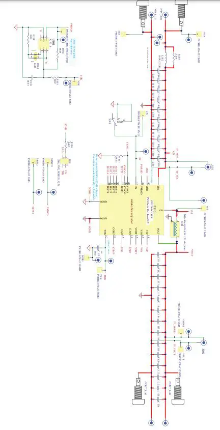
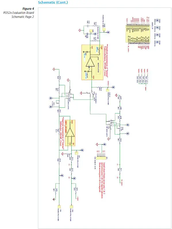
Figure 4: PI352x Evaluation Board
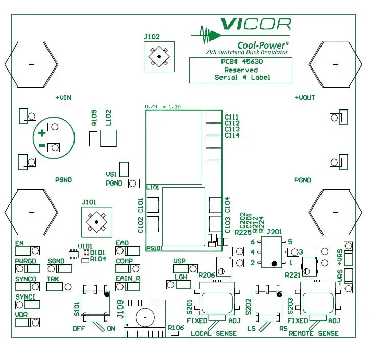
Figure 6: PI352x Evaluation Board Assembly, Bottom Side 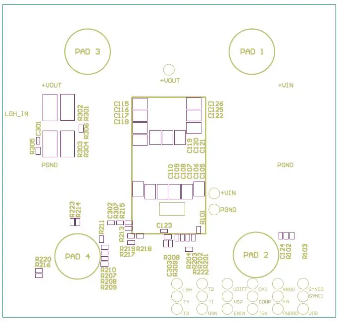
Bill of Materials
| Reference Designator | Description | QTY | Manufacturer | Manufacturer Part Number |
| C101-C110 | CAP X7R 2.2µF 10% 100V 1210 | 10 | Murata | GRM32ER72A225KA35L |
| C124 | CAP X7R .1µF 10% 100V 0603 | 1 | Murata | GRM188R72A104KA35J |
| C201 | CAP X7R 4700pF 5% 100V 0603 | 1 | TDK | C1608C0G2A472J080AC |
| CKIT | BOM CONN KIT ARRAY DEMO BD | 1 | Arnold Industries | 26647 |
| COMP, EAIN_R, EAO, EN, PWRGD, +VRS, -VRS, SGND, TRK, VDR, SYNCO, SYNCI, +VIN, PGND, +VOUT, PGND, VS1, VSP |
TEST POINT, SURFACE MOUNT |
19 |
Keystone Electronics |
5017 |
| J101, J102 | JACK VERTICAL MECH THRU HOLE | 2 | Tektronix | 131-5031-00 |
| J108 | CONN 4 POS WIRE TO BOARD SMD | 1 | AVX | 009276004021106 |
| J201 | HEADER 6 PIN STRAIGHT SMT | 1 | FCI | 95278-101A06LF |
| JMPR_1, JMPR_2, JMPR_3 | JUMPER SOCKET 2POS 2.54mm WHANDLE | 3 | TE Connectivity | 2-881545-2 |
| L102 | INDUCTOR WW 65nH 15% 19A 0404 | 1 | Eaton | FP0404R1-R065-R |
| PAD_1, PAD_2, PAD_3, PAD_4 | ADHESIVE-BACK BUMPER, 3/8″D x 7/32″H | 4 | McMaster-Carr | 95495K57 |
| R101, R106, R201, R202, R203, R204, R212, R222, R306 |
RES 0Ω JUMPER 1A 0603 |
9 |
KOA Speer |
RK73Z1JTTD |
| R102 | RES 10kΩ 1/10W 1% 0603 | 1 | KOA Speer | RK73H1JTTD1002F |
| R103 | RES 1kΩ 1/10W 1% 0603 | 1 | KOA Speer | RK73H1JTTD1001F |
| R104 | RES 2.4kΩ 1/10W 1% 0603 | 1 | KOA Speer | RK73H1JTTD2401F |
| R105 | RES 0.51Ω 1/4W 5% 1206 | 1 | KOA Speer | SR732BTTDR51J |
| R206 | RES TRIM POT 5kΩ 1/4W 10% SMD | 1 | Bourns | 3224W-1-502E |
| R211, R214 | RES 49.9Ω 1/16W 0.1% 0603 | 2 | Susumu | RG1608P-49R9-B-T5 |
| R223, R224 | RES 100Ω 1/10W 1% 0603 | 2 | KOA Speer | RK73H1JTTD1000F |
| Reference Designator | Description | QTY | Manufacturer | Manufacturer Part Number |
| S101, S202 | SW Horizontal SPDT 1 POS SMD | 2 | C&K | GT11MSABETR |
| S201, S203 | SW TOGGLE DPDT G3T22AH SMD | 2 | NKK | G3T22AH |
| TP101, TP102, TP103, TP104, TP105, TP106, TP107, TP108, TP109, TP110, TP111, TP112, TP201, TP203, TP207, TP208, TP209, TP210, TP211, TP212, TP215, TP216 |
PIN RECPT .015/.025 DIA 0667 SER TH |
22 |
Mill-Max |
0667-0-57-15-30-27-1 |
| U101 | IC SCHMITT TRIGGER INVERTER DUAL SC70-6 | 1 | Fairchild | NC7WZ14EP6X |
| C123, C202, C301, C302, C303, D101, J104, J105, J106, J107, R212, R305, R307, R308, R309 |
NOT APPLIED |
16 |
Table 4: PI352x Design Specific Components
| Reference Designator | Description | QTY | Manufacturer | Manufacturer Part Number |
| Evaluation board number: PI3525-00-EVAL1 | ||||
| PCB | SNGLTD PCB PI3525-00-EVAL1 | 1 | Vicor Power Component | 45519 |
| PS101 | COOL-POWER NI BUCK REG 60V/5V 20A | 1 | Vicor Power Component | PI3525-00-LGIZ |
| L101 | IND 230nH 10% 70A 22.2X8.2 | 1 | Eaton | FP2207R1-R230-R |
| C111-C122 | CAP X7R 47µF 10% 10V 1210 | 12 | Murata | GRM32ER71A476KE15L |
| R207 | RES 7.50Ω 1/10W 1% 0603 | 1 | KOA Speer | RK73H1JTTD7R50F |
| R208 | RES 1.18kΩ 1/10W 0.1% 0603 | 1 | Panasonic | ERA3AEB1181V |
| R209 | RES 449Ω 1/10W 0.1% 0603 | 1 | KOA Speer | RN731JTTD4990B25 |
| R210 | RES 4.81kΩ 1/10W 0.1% 0603 | 1 | Vishay | TNPW06034K81BEEA |
| R213, R219 | RES 10.2kΩ 1/10W 0.1% 0603 | 2 | Vishay | TNPW060310K2BEEA |
| R215, R218 | RES 2.74kΩ 1/16W 0.1% 0603 | 2 | Susumu | RG1608P-2741-B-T5 |
| R216 | RES 1.27kΩ 1/10W 0.1% 0603 | 1 | Vishay | TNPW06031K27BEEA |
| R217 | RES 453Ω 1/10W 0.1% 0603 | 1 | Susumu | RG1608P-4530-B-T5 |
| R220 | RES 4.64kΩ 1/16W 0.1% 0603 | 1 | Susumu | RG1608P-4641-B-T5 |
| R221 | RES TRIM POT 5kΩ 1/4W 10% SMD | 1 | Bourns | 3224W-1-502E |
| Reference Designator | Description | QTY | Manufacturer | Manufacturer Part Number |
| Evaluation board number: PI3526-00-EVAL1 | ||||
| PCB | SNGLTD PCB PI3526-00-EVAL1 | 1 | Vicor Power Component | 45630 |
| PS101 | COOL-POWER NI BUCK REG 60V/12V 18A | 1 | Vicor Power Component | PI3526-00-LGIZ |
| L101 | IND 480nH 10% 45A 17.3×14.5mm | 1 | Eaton | HCV1707R1-R48-R |
| C111-C126 | CAP X7R 10µF 10% 50V 1210 | 16 | Murata | GRM32ER71H106KA12L |
| R207 | RES 4.99Ω 1/16W 0.1% 0603 | 1 | TE | CPF0603B4R99E1 |
| R208 | RES 316Ω 1/10W 0.1% 0603 | 1 | Panasonic | ERA-3AEB3160V |
| R209 | RES 324Ω 1/10W 0.1% 0603 | 1 | Panasonic | ERA-3AEB3240V |
| R210 | RES 3.57kΩ 1/10W 0.1% 0603 | 1 | Panasonic | ERA-3AEB3571V |
| R213, R219 | RES 20kΩ 1/16W 0.1% 0603 | 2 | Susumu | RG1608P-203-B-T5 |
| R215, R218 | RES 6.12kΩ 1/16W 0.1% 0603 | 2 | Vishay | PAT0603E6121BST1 |
| R216 | RES 1.47kΩ 1/10W 1% 0603 | 1 | Panasonic | ERA3AEB1471V |
| R217 | RES 4.02kΩ 1/10W 0.1% 0603 | 1 | Panasonic | ERA-3AEB4021V |
| R220 | RES 2.49kΩ 1/16W 0.1% 0603 | 1 | Susumu | RG1608P-2491-B-T5 |
| R221 | RES TRIP POT 10kΩ 1/4W 10% SMD | 1 | Bourns | 3224W-1-103E |
| Reference Designator | Description | QTY | Manufacturer | Manufacturer Part Number |
| Evaluation board number: PI3523-00-EVAL1 | ||||
| PCB | SNGLTD PCB PI3523-00-EVAL1 | 1 | Vicor Power Component | 45519 |
| PS101 | COOL-POWER NI BUCK REG 60V/3.3V 22A | 1 | Vicor Power Component | PI3523-00-LGIZ |
| L101 | IND 230nH 10% 70A 22.2×8.2mm | 1 | Eaton | FP2207R1-R230-R |
| C111-C122 | CAP X6S 100μF 20% 6.3V 1210 | 12 | Murata | GRM32EC80J107ME20L |
| R207 | RES 7.50Ω 1/10W 1% 0603 | 1 | KOA Speer | RK73H1JTTD7R50F |
| R208 | RES 1.02kΩ 1/10W 1% 0603 | 1 | Panasonic | ERJ-3EKF1021V |
| R209 | RES 1.37KΩ 1/10W 1% 0603 | 1 | KOA Speer | RK73H1JTTD1371F |
| R210 | RES 2.4kΩ 1/10W 1% 0603 | 1 | KOA Speer | RK73H1JTTD2401F |
| R213, R215, R218, R219 | RES 18.7kΩ 1/10W 1% 0603 | 4 | KOA Speer | RK73H1JTTD1872F |
| R216 | RES 1.2kΩ 1/16W 0.1% 0603 | 1 | Susumu | RG1608P-122-B-T5 |
| R217 | RES 2.8kΩ 1/10W 1% 0603 | 1 | KOA Speer | RK73H1JTTD2801F |
| R220 | RES 1.24kΩ 1/10W 1% 0603 | 1 | KOA Speer | RK73H1JTTD1241F |
| R221 | RES TRIP POT 5kΩ 1/4W 10% SMD | 1 | Bourns | 3224W-1-502E |
Limitation of Warranties
Information in this document is believed to be accurate and reliable. HOWEVER, THIS INFORMATION IS PROVIDED “AS IS” AND WITHOUT ANY WARRANTIES, EXPRESSED OR IMPLIED, AS TO THE ACCURACY OR COMPLETENESS OF SUCH INFORMATION. VICOR SHALL HAVE NO LIABILITY FOR THE CONSEQUENCES OF USE OF SUCH INFORMATION. IN NO EVENT SHALL VICOR BE LIABLE FOR ANY INDIRECT, INCIDENTAL, PUNITIVE, SPECIAL OR CONSEQUENTIAL DAMAGES (INCLUDING, WITHOUT LIMITATION, LOST PROFITS OR SAVINGS, BUSINESS INTERRUPTION, COSTS RELATED TO THE REMOVAL OR REPLACEMENT OF ANY PRODUCTS OR REWORK CHARGES).
Vicor reserves the right to make changes to information published in this document, at any time and without notice. You should verify that this document and information is current. This document supersedes and replaces all prior versions of this publication. All guidance and content herein are for illustrative purposes only. Vicor makes no representation or warranty that the products and/or services described herein will be suitable for the specified use without further testing or modification. You are responsible for the design and operation of your applications and products using Vicor products, and Vicor accepts no liability for any assistance with applications or customer product design. It is your sole responsibility to determine whether the Vicor product is suitable and fit for your applications and products, and to implement adequate design, testing and operating safeguards for your planned application(s) and use(s).
VICOR PRODUCTS ARE NOT DESIGNED, AUTHORIZED OR WARRANTED FOR USE IN LIFE SUPPORT, LIFE-CRITICAL OR SAFETY-CRITICAL SYSTEMS OR EQUIPMENT. VICOR PRODUCTS ARE NOT CERTIFIED TO MEET ISO 13485 FOR USE IN MEDICAL EQUIPMENT NOR ISO/TS16949 FOR USE IN AUTOMOTIVE APPLICATIONS OR OTHER SIMILAR MEDICAL AND AUTOMOTIVE STANDARDS. VICOR DISCLAIMS ANY AND ALL LIABILITY FOR INCLUSION AND/OR USE OF VICOR PRODUCTS IN SUCH EQUIPMENT OR APPLICATIONS AND THEREFORE SUCH INCLUSION AND/OR USE IS AT YOUR OWN RISK.
Terms of Sale
The purchase and sale of Vicor products is subject to the Vicor Corporation Terms and Conditions of Sale which are available at: (http://www.vicorpower.com/termsconditionswarranty)
Export Control
This document as well as the item(s) described herein may be subject to export control regulations. Export may require a prior authorization from U.S. export authorities.
Contact Us: http://www.vicorpower.com/contact-us
Vicor Corporation
25 Frontage Road Andover, MA, USA 01810
Tel: 800-735-6200
Fax: 978-475-6715 www.vicorpower.com
email: Customer Service: [email protected]
Technical Support: [email protected]
©2017 – 2021 Vicor Corporation. All rights reserved. The Vicor name is a registered trademark of Vicor Corporation. All other trademarks, product names, logos and brands are property of their respective owners.


