MAXLINEAR XR77103-A0R5 Universal PMIC 3 Output Buck Regulator
Introduction
The XR77103-A0R5 evaluation board provides a platform to evaluate the features and performance of the XR77103-A0R5 Universal PMIC 3 Output Buck Regulator. The XR77103-A0R5 output voltages are set via an external resistor divider down to 0.8V with a 4.5V to 14V input voltage range, and it is packaged in a 4mm x 4mm TQFN.
Quick EVB Set Up and Start-Up
Factory Settings
The evaluation board has been set up with the following factory default configuration for quick set up and operation:
- VIN = 5.5V to 14V, optimized for a 12V input rail.
- Maximum IOUT per channel is 2A.
- 500kHz Switching frequency.
- Two channels may be paralleled for output currents up to 5A peak and 4A steady state (however additional hardware modification is required for parallel operation).
- Low power spectral density (PSM) mode operation enabled.
Quick Start Up
To quickly see the regulator in operation:
- 1. Use the factory settings and default configuration. If other settings or components are desired, apply them before the next steps. For more information, see
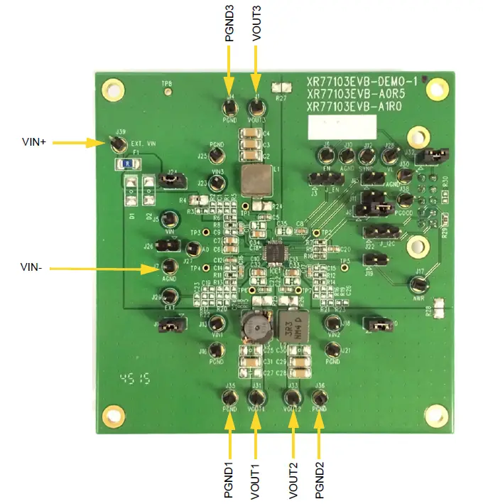
“System Set-Up” on page 5 for more. - Connect a turned-off power supply that is within the above VIN specification (from 5.5V to 14V, 12V typical) to VIN+ and VIN- with short and thick leads. Use test pins EXT. VIN (J39) and AGND (J7) to connect and monitor VIN+ and VIN- respectively. See locations in Figure 1 on page 2.
- Initially set to 0A, connect electronic loads to each desired channel that will be no more than the maximum IOUT (2A) to VOUTx and PGNDx (where x = the channel number) with short and thick leads. Use test pins in Table 1 on page 1 to connect and monitor VOUTx and PGNDx respectively. See locations in Figure 1 on page 2. For all channels with the electronic load connected, ensure that the respective VIN jumper is installed per Table 1 on page 1.
- Turn on the 12V power supply and check VOUT. The EVB powers up and regulates the enabled outputs at 3.3V (Ch1), 1.8V (Ch2) and 1.2V (Ch3) (factory default settings). PGOOD is asserted active high once sequencing is done, outputs are in regulation, and reset timer expires.
- Set or vary the load (do not exceed the maximum IOUT) and check VOUT and other desired performance levels such as regulation and efficiency. For more information about monitoring, see “I/O and Test Points” on page 4 .
Table 1: Jumper Connections for VIN, VOUT and PGND
| Channel | VI (1) N | VOUT | PGND |
| 1 | J14 | VOUT1, J31 | PGND1, J35 |
| 2 | J20 | VOUT2, J33 | PGND2, J36 |
| 3 | J24 | VOUT3, J1 | PGND3, J4 |
- Factory default: jumpers installed.
Reference Documentation
For additional information, refer to the XR77103-A0R5 data sheet, including a full list of IC features, pinout, pin descriptions, typical performance characteristics, and external component calculations.
Ordering Information
Table 2: Evaluation Board Ordering Part Number
| Evaluation Board | Board Description |
| XR77103EVB-A0R5 | XR77103-A0R5 evaluation board. |
This manual provides the EVB schematics (“XR77103EVB-A0R5 Schematic” on page 7 ), the PCB layout
(“XR77103EVB-A0R5 Schematic” on page 7 ) and the bill of materials (“XR77103EVB-A0R5 Bill of Materials” on page 10 ) that you can use on your board design.
For more information about the schematics, go to www.maxlinear.com/XR77103-A0R5.
Note: For the most up-to-date information, go to www.maxlinear.com/XR77103-A0R5.
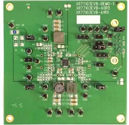
Evaluation Board Overview
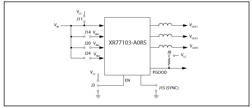
The XR77103-A0R5 EVB block diagram is shown in Figure 3.
I/O and Test Points
VIN, LX and PGOOD Test Points
Test points are available for VIN (TP8), the LX switching nodes (TP6 for LX1, TP7 for LX2, and TP1 for LX3), the compensation pins (TP4 for COMP1, TP5 for COMP2, TP3 for COMP3), and PGOOD (TP2) for monitoring.
Table 3: Test Points
| Test Point | Function |
| TP1 | LX3 |
| TP2 | PGOOD |
| TP3 | COMP3 |
| TP4 | COMP1 |
| TP5 | COMP2 |
| TP6 | LX1 |
| TP7 | LX7 |
| TP8 | VIN |
The PGOOD output can be used externally. For more information about PGOOD options, see “Jumper J8” on page 5 .
Jumper J3
Table 5: Jumper J3 Options for the EN Pin
| Jumper Options | Description |
| Jumper 1-2 (default) | The EN (enable) pin is tied to VCC and channels are enabled at power up. |
| Jumper 2-3 | The EN (enable) pin is tied to GND, permanently disabling the channels. |
| No jumper | The jumper is open, allowing EN to be controlled external to the board. |
Jumper J8
Table 6: Jumper J8 Pull Up Options for the PGOOD Pin
| Jumper Options | Description |
| Jumper 1-2 (default) | PGOOD is pulled up to the VCC pin. |
| No jumper | PGOOD is not pulled up by this jumper. |
Jumper J11
For operation from a 5V rail, it is required that the LDO output is connected to VIN, which can be accomplished by populating J11. This enhances the operation of the drivers for VIN < 5V.
Important: Remove J11 for operation at higher VIN. The board also has Zener diode placeholders which can be installed to protect the IC if higher VIN is accidentally applied.
Table 7: Jumper J11 and Operation from a 5V Rail
| Jumper Options | Description |
| Jumper 1-2 | Ties the LDO output to VIN which is required for 5V operation. |
| No jumper (default) | LDO output is not tied to VIN. |
Jumpers J14, J20 and J24
Jumpers J14, J20 and J24 are available to connect or disconnect VIN from VIN1, VIN2, and VIN3 respectively. Factory default is VIN is connected to VIN1, VIN2, and VIN3.
Jumper J15
Jumper J15 is available to ground SYNC. Factory default is that the SYNC pin is not grounded on the board. When not grounded, the SYNC pin may be connected and synchronized to an external clock in applications where EMI control is critical.
XR77103EVB-A0R5 Schematic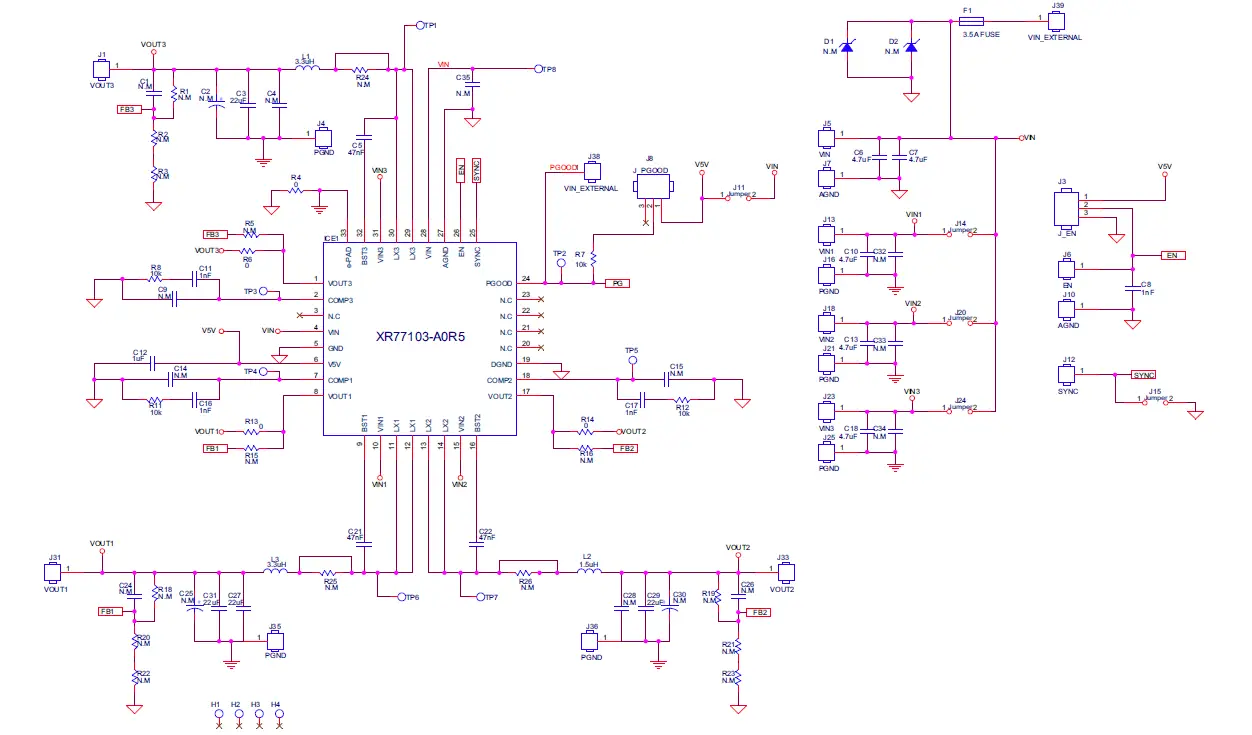
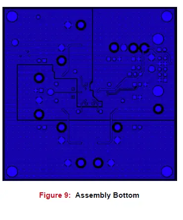
XR77103EVB-A0R5 PCB Layers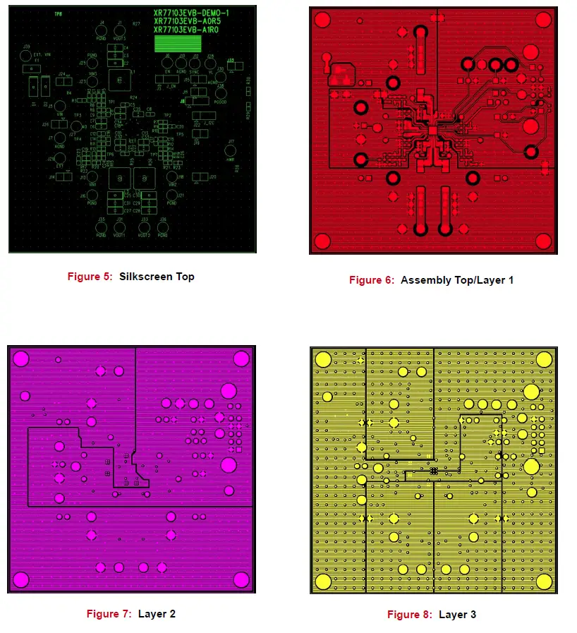
XR77103EVB-A0R5 Bill of Materials
Table 8: XR77103EVB-A0R5 Bill of Materials
| Item | Qty | Reference Designator | Component | Manufacturer / Part Number | Package Size |
| 1 | 1 | PCB | XR77103 Evaluation Board | MaxLinear | |
| 2 | 4 | C3, C27, C29, C31 | CAP CER 22uF 16V X5R 1206 10% | Murata GRM31CR61C226KE15K | 1206 |
| 3 | 3 | C5, C21, C22 | CAP CER 47nF 50V X7R 10% | Murata GRM188R71H473KA61D | 0603 |
| 4 | 5 | C6, C7, C10, C13, C18 | CAP CER 4.7uF 25V X7R 10% | Murata GRM21BR71E475KA73L | 0805 |
| 5 | 4 | C8, C11, C16, C17 | CAP CER 1nF 50V X7R 10% | Murata GRM188R71H102KA01D | 0603 |
| 6 | 1 | C12 | CAP CER 1uF, 10V, X7R, 10% | Murata GRM188R71A105KA61D | 0603 |
| 7 | 6 | R4, R6, R13, R14, R27, R28 | Resistor 0Ω, 1/10W, SMD | Panasonic ERJ-3GEY0R00V | 0603 |
| 8 | 4 | R7, R8, R11, R12 | Resistor 10.0kΩ, 1/10W, 1%, SMD | Panasonic ERJ-3EFK1002V | 0603 |
| 9 | 1 | F1 | Fuse Board Mount 3.5A, 63VDC | Vishay MFU1206FF03500P100 | 1206 |
| 10 | 20 | J1, J4, J5, J6, J7, J10, J12, J13, J16, J18, J21, J23, J25, J29, J31, J33, J35, J36, J38, J39 | Header 1-pin | Wurth Elektronik 61300111121 | 2.54mm |
| 11 | 2 | J3, J8 | Header 3-pin | Wurth Elektronik 61300311121 | 2.54mm |
| 12 | 5 | J11, J14, J15, J20, J24 | Jumper 2-pin | Wurth Elektronik 61300211121 | 2.54mm |
| 13 | 2 | L1, L3 | Inductor 3.3µH, 6A, 30mΩ, SMD | Vishay IHLP2525CZER3R3M01 | 6.86 x 6.47mm |
| 14 | 1 | L2 | Inductor 1.5µH, 9A, 15mΩ, SMD | Vishay IHLP2525CZER1R5M01 | 6.47 x 6.47mm |
| 15 | 1 | U1 | Universal PMIC 3 Output Buck Regulator | MaxLinear XR77103ELBTR-A0R5 | 4mm x 4mm |
The content of this document is furnished for informational use only, is subject to change without notice, and should not be construed as a commitment by MaxLinear, Inc. MaxLinear, Inc. assumes no responsibility or liability for any errors or inaccuracies that may appear in the informational content contained in this guide. Complying with all applicable copyright laws is the responsibility of the user. Without limiting the rights under copyright, no part of this document may be reproduced into, stored in, or introduced into a retrieval system, or transmitted in any form or by any means (electronic, mechanical, photocopying, recording, or otherwise), or for any purpose, without the express written permission of MaxLinear, Inc. Maxlinear, Inc. does not recommend the use of any of its products in life support applications where the failure or malfunction of the product can reasonably be expected to cause failure of the life support system or to significantly affect its safety or effectiveness. Products are not authorized for use in such applications unless MaxLinear, Inc. receives, in writing, assurances to its satisfaction that: (a) the risk of injury or damage has been minimized; (b) the user assumes all such risks; (c) the potential liability of MaxLinear, Inc. is adequately protected under the circumstances. MaxLinear, Inc. may have patents, patent applications, trademarks, copyrights, or other intellectual property rights covering the subject matter in this document. Except as expressly provided in any written license agreement from MaxLinear, Inc., the furnishing of this document does not give you any license to these patents, trademarks, copyrights, or other intellectual property. MaxLinear, the MaxLinear logo, any MaxLinear trademarks (XML, Full-Spectrum Capture, FSC, G.now, AirPHY, Puma, and anyway), and the MaxLinear logo on the products sold are all property of MaxLinear, Inc. or one of MaxLinear’s subsidiaries in the U.S.A. and other countries. All rights reserved. *Other company trademarks and product names appearing herein are the property of their respective owners. © 2022 MaxLinear, Inc. All rights reserved.
Corporate Headquarters: 5966 La Place Court, Suite 100 Carlsbad, CA 92008
Tel.: +1 (760) 692-0711
Fax: +1 (760) 444-8598
www.maxlinear.com


