ANALOG DEVICES LTC3311 25A Multiphase 2MHz Automotive Low EMI Buck Regulator
DESCRIPTION
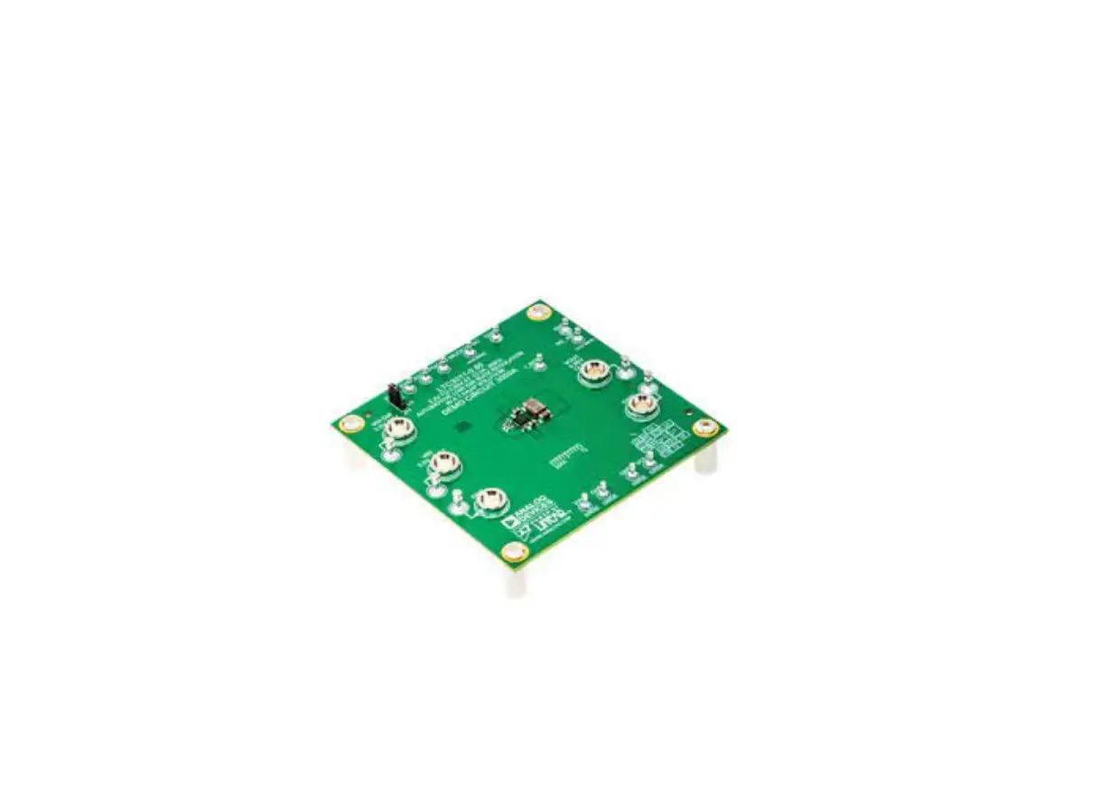
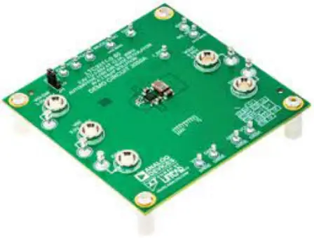
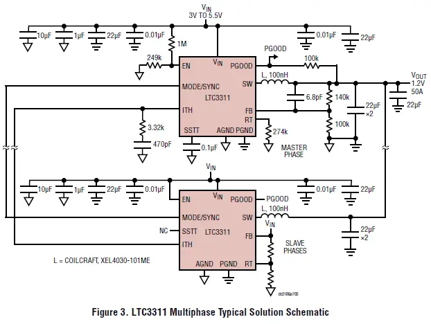
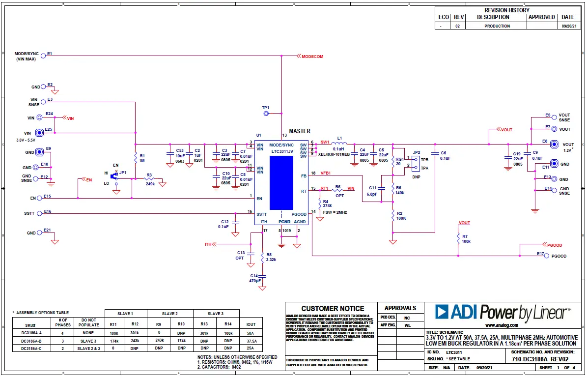
Demonstration Circuit 3186A features the LTC®3311 12.5A, low voltage synchronous step-down Silent Switcher® operating as a multiphase 2MHz, 3V to 5.5V input, 1.2V buck regulator. The DC3186A has three build options to provide a two phase 25A, three phase 37.5A, or four phase 50A output solution. The LTC3311 supports
adjustable output voltages from 0.5V to VIN and operat-ing frequencies from 500kHz up to 5MHz in multiphase operation. All phases of DC3186A operate in forced con-tinuous mode.
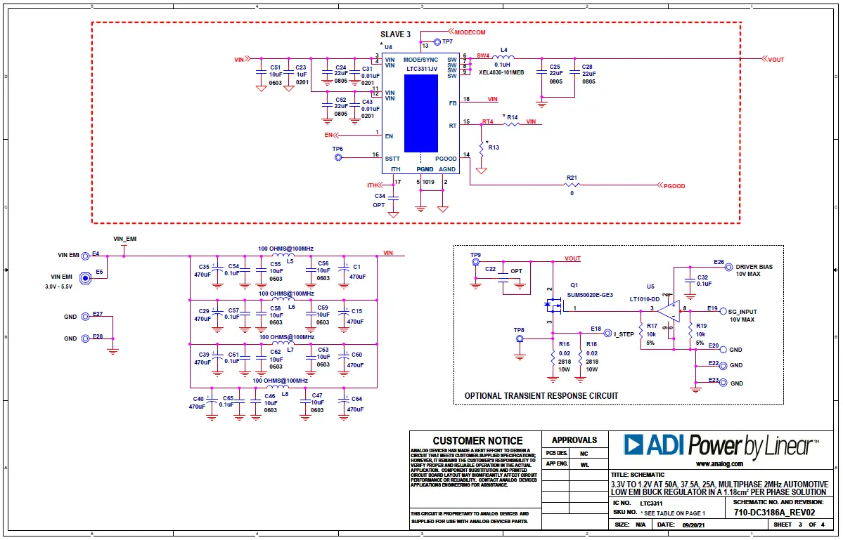
The DC3186A also has an EMI filter to reduce conducted EMI. This EMI filter can be included by applying the input voltage at the VIN EMI terminal.
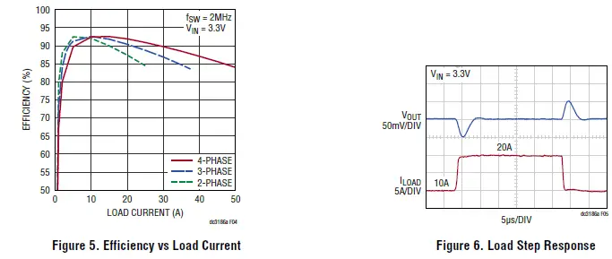
The Efficiency vs Load graph shows the efficiency of the circuit with a 3.3V input for all three build options.
An on-board transient circuit is included to measure fast transient performance.
The LTC3311 data sheet gives a complete description of the part, its operation, and application information. The data sheet must be read in conjunction with this demo manual. The LTC3311 is assembled in a 3mm × 3mm LQFN package with exposed pads for low thermal resistance.
Design files for this circuit board are available.
All registered trademarks and trademarks are the property of their respective owners.
PERFORMANCE SUMMARY
Specifications are at TA = 25°C
| SYMBOL | PARAMETER | CONDITIONS | MIN. | TYP. | MAX. | UNITS | |
| VIN/VIN EMI | DC3186A Input Voltage Range | 3 | 5.5 | V | |||
| VOUT | DC3186A Output Voltage Range | 1.176 | 1.2 | 1.224 | V | ||
| IOUT | DC3186A Output Current | DC3186A-A, 4-Phase Build Option, VIN ≥ 3V DC3186A-B, 3-Phase Build Option, VIN ≥ 3V | 50 37.5 | A A | |||
| 25 | A | ||||||
| DC3186A-C, 2-Phase Build Option, VIN ≥ 3V | |||||||
| fSW | Switching Frequency | 1.8 | 2.2 | MHz | |||
| EFF | Efficiency | VIN = 3.3V, IOUT = 15A, 4-Phase | 92.5 | % | |||
QUICK START PROCEDURE
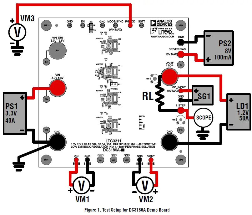
Refer to Figure 1 for the proper measurement equipment setup and follow the procedure below:
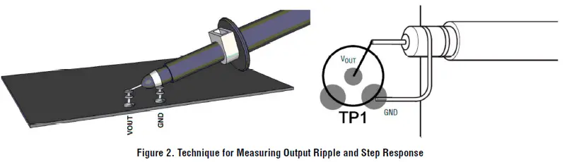
NOTE: For accurate VIN, VOUT and efficiency measurements, measure VIN at the VIN SNSE and GND SNSN turrets, and measure VOUT at the VOUT SNSE and GND SNSE turrets, as illustrated as VM1 and VM2 in Figure 1. When measuring the input or output ripple, care must be taken to avoid a long ground lead on the oscilloscope probe. Measure the output voltage ripple by touching the probe tip directly across the output turrets or to TP1 as shown in Figure 2.
- Set the JP1 Jumper to the HI position.
- With power off, connect the input power supply to VIN and GND. If the input EMI filter is desired, connect the input power supply to VIN EMI and GND.
- Set power supply PS1 current limit to 40A. Set the electronic load LD1 to CC mode and 0A current. Slowly increase PS1 to 1V. If PS1 output current reads less than 20mA, increase PS1 to 3.3V. Verify that VM1 reads 3.3V and VM2 reads 1.2V. Check VM1, VM2, VM3, PS1 output current, and LD1 input current. Connect an oscilloscope voltage probe as shown in Figure 2. Set Channel to AC-coupled, voltage scale to 20mV and time base to 10µs. Check VOUT ripple voltage. Verify that PGOOD voltage is above 3V.
- Increase the load by 1A intervals up to full load and observe the voltage output regulation, ripple voltage.
- To test the transient response with a base load, add the desired resistor to produce a minimum load between VOUT and I_STEP turrets (RL shown on Figure 1).
Note that the total load resistance will be RL plus R16 (10mΩ). The DC3186A uses a buffered signal generator input to drive a source follower circuit, and to control the slew rate and amplitude of the current transient. The source follower FET, Q1, operates in the linear region during the load step. - Connect PS2 to DRIVER BIAS and GND turrets. Turn on and set PS2 to 8V.
- Set a signal generator with a 1ms pulse width, a 10ms period and an amplitude from 0V to 4V, and then connect it to SG_INPUT turret.
NOTE: Do not allow the pulse generator to have more than a 20% duty cycle. This can allow too much power to be dissipated in Q1 and can damage the FET. - Connect an oscilloscope with a time scale of 200µs/div with one channel having a vertical scale of 2V/div on the SG_INPUT and another with a vertical scale of 50mV/div to the I_STEP turret.
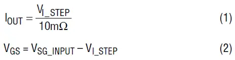
- Measure the I_STEP voltage to observe the current, VI_STEP/10mΩ. Adjust the amplitude of the pulse to provide the desired transient. Adjust the rising and falling edge of the pulse to provide the desired ramp rate. Figure 5 shows a load step from 10A to 20A in 1µs. Refer to the following equations:

- When done, turn off SG1, PS1 and Load. Remove all the connections to the demo board.
TEST SETUP
TYPICAL PERFORMANCE CHARACTERISTICS
THEORY OF OPERATION
Introduction to the DC3186A
The DC3186A demonstration circuit features the LTC3311, an automotive grade low voltage synchronous step-down Silent Switcher in a two, three, or four phase operation. The LTC3311 is a monolithic, constant frequency, current mode step-down DC/DC converter. Connecting the RT pin of the master phase with a resistor to AGND programs
the frequency from 500kHz to 5MHz. With RT resistor on master phase, the MODE/SYNC pin becomes a clock output to drive the MODE/SYNC pins of the slave phases. The DC3186A can operate with an external clock by short-ing the master phase RT pin to VIN with a 0Ω resistor in the R5 location and applying a clock signal on the MODE/SYNC turret. If the EN pin is low, the LTC3311 is in shut down and in a low quiescent current state. When the EN pin is above its threshold, the switching regulator will be enabled.
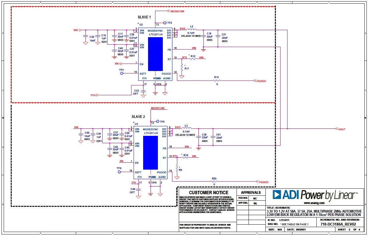
Connecting the FB pin to VIN configures a phase as a slave. The MODE/SYNC pin becomes an input, and the voltage control loop is disabled. The current control loop in the slave phase is still active, and the peak current is controlled via the shared ITH node. The phasing of a slave phase relative to the master phase is programmed with a resistor divider on the RT pin. Refer to Table 5 of the data sheet for more information on setting the slave phase angle.
In the multiphase application, the LTC3311 operates in forced continuous mode. At light loads, the slave phases will continue to operate in forced continuous mode.
Setting the compensation for the multiphase is similar to setting the compensation to the single phase. When designing the compensation network, controlling the loop stability and transient response are the two main consideration. The LTC3311 has been designed to operate at a high bandwidth for fast transient response capabili-ties. This reduces output capacitance required to meet the desired transient voltage range. The mid-band gain of the loop increases with R8 and the bandwidth of the loop increases with decreasing C14. C11 along with R6 provides a phase lead which will improve the phase mar-gin. C13, C33, C34, and C44 along with R8 provides a high frequency pole to reduce the high frequency gain. C13, C33, C34, and C44 are in parallel on the ITH node. The sum of these caps will be the total capacitance on the master phase ITH pin. Too much capacitance will slow down the response time.
Loop stability is generally measured using the Bode Plot method of plotting loop gain in dB and phase shift in degrees. The 0dB crossover frequency should be less the 1/6 of the operating frequency to reduce the effects of added phase shift of the modulator. The control loop phase margin goal should be 45° or greater and a gain margin goal of 8dB or greater. Refer to the LTC3311 data sheet and LTPowerCAD for more information on choosing the required components.
The soft-start of the multiphase regulator is controlled by a single cap, C12, on the master phase. After the regulator is in regulation the SSTT pin can be used to monitor the temperature of each IC. The master phase temperature can be monitored at the SSTT turret and slave 1, 2, and 3 can be monitored at TP3, 4, and 6 respectively. Calculate the die temperature with the formula below:
PARTS LIST
| ITEM | QTY REFERENCE | PART DESCRIPTION | MANUFACTURER/PART NUMBER |
DC3186A-A Required Circuit Components
| 1 | 4 | C2, C16, C23, C36 | CAP., 1µF, X7T, 6.3V, 20%, 0201 | MURATA, GRM033D70J105ME01D |
| 2 | 17 | C3-C5, C10, C17-C19, C21, C24, C25, C28, C37, C38, C41, C42, C49, C52 | CAP., 22µF, X7S, 6.3V, 20%, 0805 | TDK, C2012X7S0J226M125AC |
| 3 | 2 | C6, C12 | CAP., 0.1µF, X7R, 16V, 10%, 0402, AEC-Q200 | MURATA, GCM155R71C104KA55D |
| 4 | 8 | C7, C8, C20, C26, C27, C31, C43, C45 | CAP., 0.01µF, X7R, 6.3V, 10%, 0201 | AVX, 02016C103KAT2A |
| 5 | 1 | C11 | CAP., 6.8pF, C0G/NP0, 50V, ±0.5pF, 0402 | AVX, 04025A6R8DAT2A |
| 6 | 1 | C14 | CAP., 470pF, C0G, 50V, 5%, 0402, AEC-Q200 | TDK, CGA2B2C0G1H471J050BA |
| 7 | 4 | C30, C50, C51, C53 | CAP., 10µF, X7S, 6.3V, 20%, 0603 | TDK, C1608X7S0J106M080AC |
| 8 | 4 | L1-L4 | IND., 0.1µH, PWR, SHIELDED, 20%, 25.8A, 1.8mΩ, 4.3mm × 4.3mm, XEL4030, AEC-Q200 | COILCRAFT, XEL4030-101MEB |
| 9 | 1 | R1 | RES., 1M, 1%, 1/16W, 0402, AEC-Q200 | STACKPOLE ELECTRONICS, INC., RMCF0402FT1M00 |
| 10 | 3 | R2, R11, R14 | RES., 100k, 1%, 1/16W, 0402, AEC-Q200 | NIC, NRC04F1003TRF |
| 11 | 1 | R3 | RES., 249k, 1%, 1/16W, 0402, AEC-Q200 | NIC, NRC04F2493TRF |
| 12 | 1 | R4 | RES., 274k, 1%, 1/16W, 0402, AEC-Q200 | NIC, NRC04F2743TRF |
| 13 | 1 | R6 | RES., 140k, 1%, 1/16W, 0402, AEC-Q200 | NIC, NRC04F1403TRF |
| 14 | 1 | R7 | RES., 100k, 5%, 1/16W, 0402, AEC-Q200 | NIC, NRC04J104TRF |
| 15 | 1 | R8 | RES., 3.32k, 1%, 1/10W, 0402, AEC-Q200 | PANASONIC, ERJ2RKF3321X |
| 16 | 4 | R9, R15, R20, R21 | RES., 0Ω, 1/16W, 0402 | VISHAY, CRCW04020000Z0ED |
| 17 | 2 | R12, R13 | RES., 301k, 1%, 1/16W, 0402 | SAMSUNG, RC1005F3013CS |
| 18 | 4 | U1-U4 | IC, LOW VOLTAGE SYN. STEPDOWN REG, LQFN-18 | ANALOG DEVICES, LTC3311JV#PBF |
Additional Demo Board Circuit Components
| 1 | 8 | C1, C15, C29, C35, C39, C40, C60, C64 | CAP., 470µF, TANT POLY, 6.3V, 20%, 7343 | PANASONIC, 6TCE470MI |
| 2 | 6 | C9, C32, C54, C57, C61, C65 | CAP., 0.1µF, X7R, 16V, 10%, 0402, AEC-Q200 | MURATA, GCM155R71C104KA55D |
| 3 | 8 | C46, C47, C55, C56, C58, C59, C62, C63 | CAP., 10µF, X7S, 6.3V, 20%, 0603 | TDK, C1608X7S0J106M080AC |
| 4 | 4 | L5-L8 | IND., 100Ω AT 100MHz, FERRITE BEAD, 25%, 8A, 6mΩ, 1812 | WURTH ELEKTRONIK, 74279226101 |
| 5 | 1 | Q1 | XSTR., MOSFET, N-CH, 60V, 120A, TO-263 | VISHAY, SUM50020E-GE3 |
| 6 | 2 | R16, R18 | RES., 0.02Ω, 1%, 10W, 2818, HP, METAL, SENSE, AEC-Q200 | VISHAY, WSHP2818R0200FEA |
| ITEM | QTY REFERENCE | PART DESCRIPTION | MANUFACTURER/PART NUMBER |
| 7 | 2 R17, R19 | RES., 10k, 5%, 1/16W, 0402, AEC-Q200 | NIC, NRC04J103TRF |
| 8 | 1 RG1 | RES., 20Ω, 1%, 1/16W, 0402, AEC-Q200 | NIC, NRC04F20R0TRF |
| 9 | 1 U5 | IC, OPAMP BUFFER, 20MHz, ±150mA, DFN-8 | ANALOG DEVICES, LT1010CDD#PBF |
Hardware: For Demo Board Only
| 1 | 12 | E1-E3, E5, E12, E14-E17, E19-E21 | TEST POINT, TURRET, 0.064″ MTG. HOLE, PCB 0.062″ THK | MILL-MAX, 2308-2-00-80-00-00-07-0 |
| 2 | 11 | E4, E7, E10, E13, E18, E22-E24, E26-E28 | TEST POINT, TURRET, 0.094″ MTG. HOLE, PCB 0.062″ THK | MILL-MAX, 2501-2-00-80-00-00-07-0 |
| 3 | 5 | E6, E8, E9, E11, E25 | STUD, #10-32, FASTENER, 0.625″ LENGTH | PENCOM, PR1422 |
| 4 | 1 | JP1 | CONN., HDR, MALE, 1 × 3, 2mm, VERT, ST, THT | WURTH ELEKTRONIK, 62000311121 |
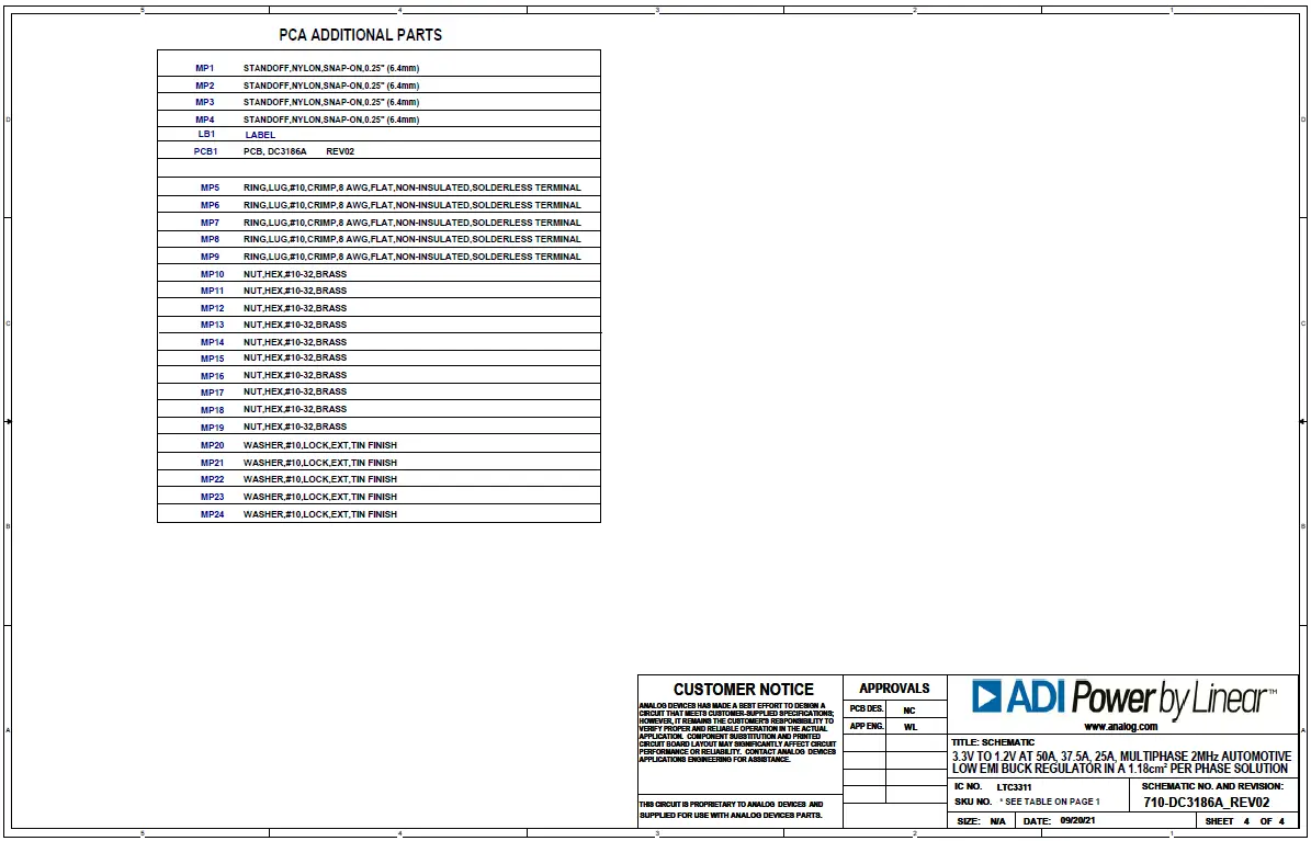
| 5 | 4 | MP1-MP4 | STANDOFF, NYLON, SNAP-ON, 0.25″ (6.4mm) | KEYSTONE, 8831 |
| 6 | 5 | MP5-MP9 | RING, LUG, #10, CRIMP, 8 AWG, FLAT, NON- INSULATED, SOLDERLESS TERMINAL | MOLEX, 0192210223 |
| 7 | 10 | MP10-MP19 | NUT, HEX, #10-32, BRASS | PENCOM, NU1132 |
| 8 | 5 | MP20-MP24 | WASHER, #10, LOCK, EXT, TIN FINISH | PENCOM, WA4526 |
| 9 | 1 | XJP1 | CONN., SHUNT, FEMALE, 2-POS, 2mm | WURTH ELEKTRONIK, 60800213421 |
DC3186A-B Required Circuit Components
| 1 | 3 | C2, C16, C36 | CAP., 1µF, X7T, 6.3V, 20%, 0201 | MURATA, GRM033D70J105ME01D |
| 2 | 13 | C3-C5, C10, C17-C19, C21, C37, C38, C41, C42, C49 | CAP., 22µF, X7S, 6.3V, 20%, 0805 | TDK, C2012X7S0J226M125AC |
| 3 | 2 | C6, C12 | CAP., 0.1µF, X7R, 16V, 10%, 0402, AEC-Q200 | MURATA, GCM155R71C104KA55D |
| 4 | 6 | C7, C8, C20, C26, C27, C45 | CAP., 0.01µF, X7R, 6.3V, 10%, 0201 | AVX, 02016C103KAT2A |
| 5 | 1 | C11 | CAP., 6.8pF, C0G/NP0, 50V, ±0.5pF, 0402 | AVX, 04025A6R8DAT2A |
| 6 | 1 | C14 | CAP., 470pF, C0G, 50V, 5%, 0402, AEC-Q200 | TDK, CGA2B2C0G1H471J050BA |
| 7 | 3 | C30, C50, C53 | CAP., 10µF, X7S, 6.3V, 20%, 0603 | TDK, C1608X7S0J106M080AC |
| 8 | 3 | L1-L3 | IND., 0.1µH, PWR, SHIELDED, 20%, 25.8A, 1.8mΩ, 4.3mm × 4.3mm, XEL4030, AEC-Q200 | COILCRAFT, XEL4030-101MEB |
| 9 | 1 | R1 | RES., 1M, 1%, 1/16W, 0402, AEC-Q200 | STACKPOLE ELECTRONICS, INC., RMCF0402FT1M00 |
| 10 | 1 | R2 | RES., 100k, 1%, 1/16W, 0402, AEC-Q200 | NIC, NRC04F1003TRF |
| 11 | 1 | R3 | RES., 249k, 1%, 1/16W, 0402, AEC-Q200 | NIC, NRC04F2493TRF |
| 12 | 1 | R4 | RES., 274k, 1%, 1/16W, 0402, AEC-Q200 | NIC, NRC04F2743TRF |
| 13 | 1 | R6 | RES., 140k, 1%, 1/16W, 0402, AEC-Q200 | NIC, NRC04F1403TRF |
| 14 | 1 | R7 | RES., 100k, 5%, 1/16W, 0402, AEC-Q200 | NIC, NRC04J104TRF |
| 15 | 1 | R8 | RES., 3.32k, 1%, 1/10W, 0402, AEC-Q200 | PANASONIC, ERJ2RKF3321X |
| 16 | 2 | R9, R12 | RES., 243k, 1%, 1/16W, 0402, AEC-Q200 | NIC, NRC04F2433TRF |
| 17 | 2 | R10, R11 | RES., 174k, 1%, 1/16W, 0402, AEC-Q200 | NIC, NRC04F1743TRF |
| 18 | 2 | R15, R20 | RES., 0Ω, 1/16W, 0402 | VISHAY, CRCW04020000Z0ED |
| 19 | 3 | U1-U3 | IC, LOW VOLTAGE SYN. STEPDOWN REG, LQFN-18 | ANALOG DEVICES, LTC3311JV#PBF |
| ITEM | QTY REFERENCE | PART DESCRIPTION | MANUFACTURER/PART NUMBER |
Additional Demo Board Circuit Components
| 1 | 5 | C9, C32, C57, C61, C65 | CAP., 0.1µF, X7R, 16V, 10%, 0402, AEC-Q200 | MURATA, GCM155R71C104KA55D |
| 2 | 6 | C15, C29, C39, C40, C60, C64 | CAP., 470µF, TANT POLY, 6.3V, 20%, 7343 | PANASONIC, 6TCE470MI |
| 3 | 6 | C46, C47, C58, C59, C62, C63 | CAP., 10µF, X7S, 6.3V, 20%, 0603 | TDK, C1608X7S0J106M080AC |
| 4 | 3 | L6-L8 | IND., 100Ω AT 100MHz, FERRITE BEAD, 25%, 8A, 6mΩ, 1812 | WURTH ELEKTRONIK, 74279226101 |
| 5 | 1 | Q1 | XSTR., MOSFET, N-CH, 60V, 120A, TO-263 | VISHAY, SUM50020E-GE3 |
| 6 | 2 | R16, R18 | RES., 0.02Ω, 1%, 10W, 2818, HP, METAL, SENSE, AEC-Q200 | VISHAY, WSHP2818R0200FEA |
| 7 | 2 | R17, R19 | RES., 10k, 5%, 1/16W, 0402, AEC-Q200 | NIC, NRC04J103TRF |
| 8 | 1 | RG1 | RES., 20Ω, 1%, 1/16W, 0402, AEC-Q200 | NIC, NRC04F20R0TRF |
| 9 | 1 | U5 | IC, OPAMP BUFFER, 20MHz, ±150mA, DFN-8 | ANALOG DEVICES, LT1010CDD#PBF |
Hardware: For Demo Board Only
| 1 | 12 | E1-E3, E5, E12, E14-E17, E19-E21 | TEST POINT, TURRET, 0.064″ MTG. HOLE, PCB 0.062″ THK | MILL-MAX, 2308-2-00-80-00-00-07-0 |
| 2 | 11 | E4, E7, E10, E13, E18, E22-E24, E26-E28 | TEST POINT, TURRET, 0.094″ MTG. HOLE, PCB 0.062″ THK | MILL-MAX, 2501-2-00-80-00-00-07-0 |
| 3 | 5 | E6, E8, E9, E11, E25 | STUD, #10-32, FASTENER, 0.625″ LENGTH | PENCOM, PR1422 |
| 4 | 1 | JP1 | CONN., HDR, MALE, 1 × 3, 2mm, VERT, ST, THT | WURTH ELEKTRONIK, 62000311121 |
| 5 | 4 | MP1-MP4 | STANDOFF, NYLON, SNAP-ON, 0.25″ (6.4mm) | KEYSTONE, 8831 |
| 6 | 5 | MP5-MP9 | RING, LUG, #10, CRIMP, 8 AWG, FLAT, NON- INSULATED, SOLDERLESS TERMINAL | MOLEX, 0192210223 |
| 7 | 10 | MP10-MP19 | NUT, HEX, #10-32, BRASS | PENCOM, NU1132 |
| 8 | 5 | MP20-MP24 | WASHER, #10, LOCK, EXT, TIN FINISH | PENCOM, WA4526 |
| 9 | 1 | XJP1 | CONN., SHUNT, FEMALE, 2-POS, 2mm | WURTH ELEKTRONIK, 60800213421 |
DC3186A-C Required Circuit Components
| 1 | 2 | C2, C16 | CAP., 1µF, X7T, 6.3V, 20%, 0201 | MURATA, GRM033D70J105ME01D |
| 2 | 9 | C3-C5, C10, C17-C19, C21, C49 | CAP., 22µF, X7S, 6.3V, 20%, 0805 | TDK, C2012X7S0J226M125AC |
| 3 | 2 | C6, C12 | CAP., 0.1µF, X7R, 16V, 10%, 0402, AEC-Q200 | MURATA, GCM155R71C104KA55D |
| 4 | 4 | C7, C8, C26, C27 | CAP., 0.01µF, X7R, 6.3V, 10%, 0201 | AVX, 02016C103KAT2A |
| 5 | 1 | C11 | CAP., 6.8pF, C0G/NP0, 50V, ±0.5pF, 0402 | AVX, 04025A6R8DAT2A |
| 6 | 1 | C14 | CAP., 470pF, C0G, 50V, 5%, 0402, AEC-Q200 | TDK, CGA2B2C0G1H471J050BA |
| 7 | 2 | C30, C53 | CAP., 10µF, X7S, 6.3V, 20%, 0603 | TDK, C1608X7S0J106M080AC |
| 8 | 2 | L1, L2 | IND., 0.1µH, PWR, SHIELDED, 20%, 25.8A, 1.8mΩ, 4.3mm × 4.3mm, XEL4030, AEC-Q200 | COILCRAFT, XEL4030-101MEB |
| 9 | 1 | R1 | RES., 1M, 1%, 1/16W, 0402, AEC-Q200 | STACKPOLE ELECTRONICS, INC., RMCF0402FT1M00 |
| 10 | 1 | R2 | RES., 100k, 1%, 1/16W, 0402, AEC-Q200 | NIC, NRC04F1003TRF |
| 11 | 1 | R3 | RES., 249k, 1%, 1/16W, 0402, AEC-Q200 | NIC, NRC04F2493TRF |
| ITEM | QTY REFERENCE | PART DESCRIPTION | MANUFACTURER/PART NUMBER | |
| 12 | 1 | R4 | RES., 274k, 1%, 1/16W, 0402, AEC-Q200 | NIC, NRC04F2743TRF |
| 13 | 1 | R6 | RES., 140k, 1%, 1/16W, 0402, AEC-Q200 | NIC, NRC04F1403TRF |
| 14 | 1 | R7 | RES., 100k, 5%, 1/16W, 0402, AEC-Q200 | NIC, NRC04J104TRF |
| 15 | 1 | R8 | RES., 3.32k, 1%, 1/10W, 0402, AEC-Q200 | PANASONIC, ERJ2RKF3321X |
| 16 | 2 | R11, R15 | RES., 0Ω, 1/16W, 0402 | VISHAY, CRCW04020000Z0ED |
| 17 | 2 | U1, U2 | IC, LOW VOLTAGE SYN. STEPDOWN REG, LQFN-18 | ANALOG DEVICES, LTC3311JV#PBF |
Additional Demo Board Circuit Components
| 1 | 4 | C9, C32, C57, C61 | CAP., 0.1µF, X7R, 16V, 10%, 0402, AEC-Q200 | MURATA, GCM155R71C104KA55D |
| 2 | 4 | C15, C29, C39, C60 | CAP., 470µF, TANT POLY, 6.3V, 20%, 7343 | PANASONIC, 6TCE470MI |
| 3 | 4 | C58, C59, C62, C63 | CAP., 10µF, X7S, 6.3V, 20%, 0603 | TDK, C1608X7S0J106M080AC |
| 4 | 2 | L6, L7 | IND., 100Ω AT 100MHz, FERRITE BEAD, 25%, 8A, 6mΩ, 1812 | WURTH ELEKTRONIK, 74279226101 |
| 5 | 1 | Q1 | XSTR., MOSFET, N-CH, 60V, 120A, TO-263 | VISHAY, SUM50020E-GE3 |
| 6 | 2 | R16, R18 | RES., 0.02Ω, 1%, 10W, 2818, HP, METAL, SENSE, AEC-Q200 | VISHAY, WSHP2818R0200FEA |
| 7 | 2 | R17, R19 | RES., 10k, 5%, 1/16W, 0402, AEC-Q200 | NIC, NRC04J103TRF |
| 8 | 1 | RG1 | RES., 20Ω, 1%, 1/16W, 0402, AEC-Q200 | NIC, NRC04F20R0TRF |
| 9 | 1 | U5 | IC, OPAMP BUFFER, 20MHz, ±150mA, DFN-8 | ANALOG DEVICES, LT1010CDD#PBF |
Hardware: For Demo Board Only
| 1 | 12 | E1-E3, E5, E12, E14-E17, E19-E21 | TEST POINT, TURRET, 0.064″ MTG. HOLE, PCB 0.062″ THK | MILL-MAX, 2308-2-00-80-00-00-07-0 |
| 2 | 11 | E4, E7, E10, E13, E18, E22-E24, E26-E28 | TEST POINT, TURRET, 0.094″ MTG. HOLE, PCB 0.062″ THK | MILL-MAX, 2501-2-00-80-00-00-07-0 |
| 3 | 5 | E6, E8, E9, E11, E25 | STUD, #10-32, FASTENER, 0.625″ LENGTH | PENCOM, PR1422 |
| 4 | 1 | JP1 | CONN., HDR, MALE, 1×3, 2mm, VERT, ST, THT | WURTH ELEKTRONIK, 62000311121 |
| 5 | 4 | MP1-MP4 | STANDOFF, NYLON, SNAP-ON, 0.25″ (6.4mm) | KEYSTONE, 8831 |
| 6 | 5 | MP5-MP9 | RING, LUG, #10, CRIMP, 8 AWG, FLAT, NON- INSULATED, SOLDERLESS TERMINAL | MOLEX, 0192210223 |
| 7 | 10 | MP10-MP19 | NUT, HEX, #10-32, BRASS | PENCOM, NU1132 |
| 8 | 5 | MP20-MP24 | WASHER, #10, LOCK, EXT, TIN FINISH | PENCOM, WA4526 |
| 9 | 1 | XJP1 | CONN., SHUNT, FEMALE, 2-POS, 2mm | WURTH ELEKTRONIK, 60800213421 |
SCHEMATIC DIAGRAM
Information furnished by Analog Devices is believed to be accurate and reliable. However, no responsibility is assumed by Analog Devices for its use, nor for any infringements of patents or other rights of third parties that may result from its use. Specifications subject to change without notice. No license is granted by implication or otherwise under any patent or patent rights of Analog Devices.
ESD Caution
ESD (electrostatic discharge) sensitive device. Charged devices and circuit boards can discharge without detection. Although this product features patented or proprietary protection circuitry, damage may occur on devices subjected to high-energy ESD. Therefore, proper ESD precautions should be taken to avoid performance degradation or loss of functionality.
Legal Terms and Conditions
By using the evaluation board discussed herein (together with any tools, components documentation or support materials, the “Evaluation Board”), you are agreeing to be bound by the terms and conditions set forth below (“Agreement”) unless you have purchased the Evaluation Board, in which case the Analog Devices Standard Terms and Conditions of Sale shall govern. Do not use the Evaluation Board until you have read and agreed to the Agreement. Your use of the Evaluation Board shall signify your acceptance of the Agreement. This Agreement is made by and between you (“Customer”) and Analog Devices, Inc. (“ADI”), with its principal place of business at One Technology Way, Norwood, MA 02062, USA. Subject to the terms and conditions of the Agreement, ADI hereby grants to Customer a free, limited, personal, temporary, non-exclusive, non-sublicensable, non-transferable license to use the Evaluation Board FOR EVALUATION PURPOSES ONLY. Customer understands and agrees that the Evaluation Board is provided for the sole and exclusive purpose referenced above, and agrees not to use the Evaluation Board for any other purpose. Furthermore, the license granted is expressly made subject to the following additional limitations: Customer shall not (i) rent, lease, display, sell, transfer, assign, sublicense, or distribute the Evaluation Board; and (ii) permit any Third Party to access the Evaluation Board. As used herein, the term “Third Party” includes any entity other than ADI, Customer, their employees, affiliates and in-house consultants. The Evaluation Board is NOT sold to Customer; all rights not expressly granted herein, including ownership of the Evaluation Board, are reserved by ADI. CONFIDENTIALITY. This Agreement and the Evaluation Board shall all be considered the confidential and proprietary information of ADI. Customer may not disclose or transfer any portion of the Evaluation Board to any other party for any reason. Upon discontinuation of use of the Evaluation Board or termination of this Agreement, Customer agrees to promptly return the Evaluation Board to ADI. ADDITIONAL RESTRICTIONS. Customer may not disassemble, decompile or reverse engineer chips on the Evaluation Board. Customer shall inform ADI of any occurred damages or any modifications or alterations it makes to the Evaluation Board, including but not limited to soldering or any other activity that affects the material content of the Evaluation Board. Modifications to the Evaluation Board must comply with applicable law, including but not limited to the RoHS Directive. TERMINATION. ADI may terminate this Agreement at any time upon giving written notice to Customer. Customer agrees to return to ADI the Evaluation Board at that time.
LIMITATION OF LIABILITY. THE EVALUATION BOARD PROVIDED HEREUNDER IS PROVIDED “AS IS” AND ADI MAKES NO WARRANTIES OR REPRESENTATIONS OF ANY KIND WITH RESPECT TO IT. ADI SPECIFICALLY DISCLAIMS ANY REPRESENTATIONS, ENDORSEMENTS, GUARANTEES, OR WARRANTIES, EXPRESS OR IMPLIED, RELATED TO THE EVALUATION BOARD INCLUDING, BUT NOT LIMITED TO, THE IMPLIED WARRANTY OF MERCHANTABILITY, TITLE, FITNESS FOR A PARTICULAR PURPOSE OR NONINFRINGEMENT OF INTELLECTUAL PROPERTY RIGHTS. IN NO EVENT WILL ADI AND ITS LICENSORS BE LIABLE FOR ANY INCIDENTAL, SPECIAL, INDIRECT, OR CONSEQUENTIAL DAMAGES RESULTING FROM CUSTOMER’S POSSESSION OR USE OF THE EVALUATION BOARD, INCLUDING BUT NOT LIMITED TO LOST PROFITS, DELAY COSTS, LABOR COSTS OR LOSS OF GOODWILL. ADI’S TOTAL LIABILITY FROM ANY AND ALL CAUSES SHALL BE LIMITED TO THE AMOUNT OF ONE HUNDRED US DOLLARS ($100.00).
EXPORT. Customer agrees that it will not directly or indirectly export the Evaluation Board to another country, and that it will comply with all applicable United States federal laws and regulations relating to exports. GOVERNING LAW. This Agreement shall be governed by and construed in accordance with the substantive laws of the Commonwealth of Massachusetts (excluding conflict of law rules). Any legal action regarding this Agreement will be heard in the state or federal courts having jurisdiction in Suffolk County, Massachusetts, and Customer hereby submits to the personal jurisdiction and venue of such courts. The United Nations Convention on Contracts for the International Sale of Goods shall not apply to this Agreement and is expressly disclaimed.
ANALOG DEVICES, INC. 2022
09/22
www.analog.com


