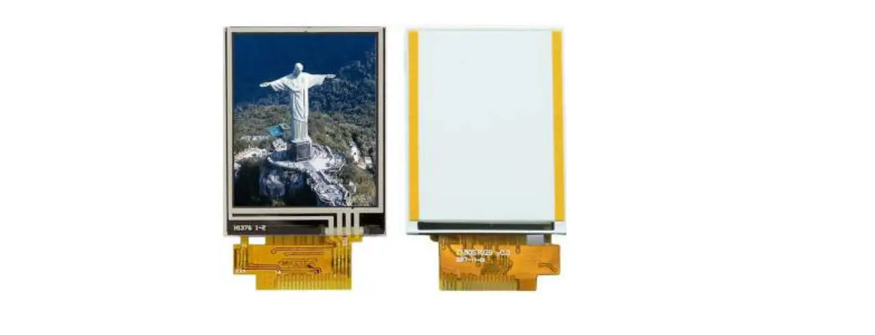
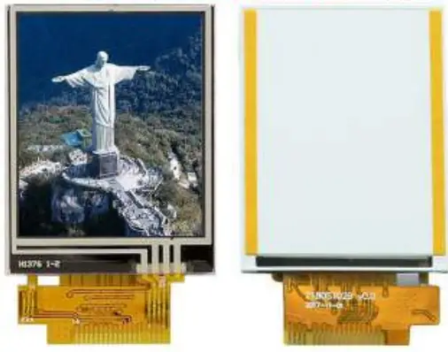
Surenoo STP0177F-128160 Series TFT Touch LCD Panel
General Description
| MODEL NO
| STP0177F-128160 |
| Display Mode
| Transmissive |
| Display Format
| Graphic 128RGB*160 Dot-matrix |
| Input Data
| SPI-4wire interface |
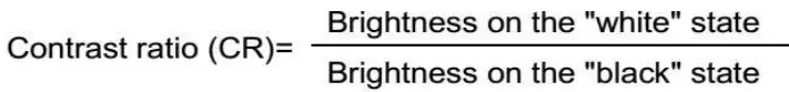
| Viewing Direction
| 12 o’clock |
| Drive
| ST7735S |
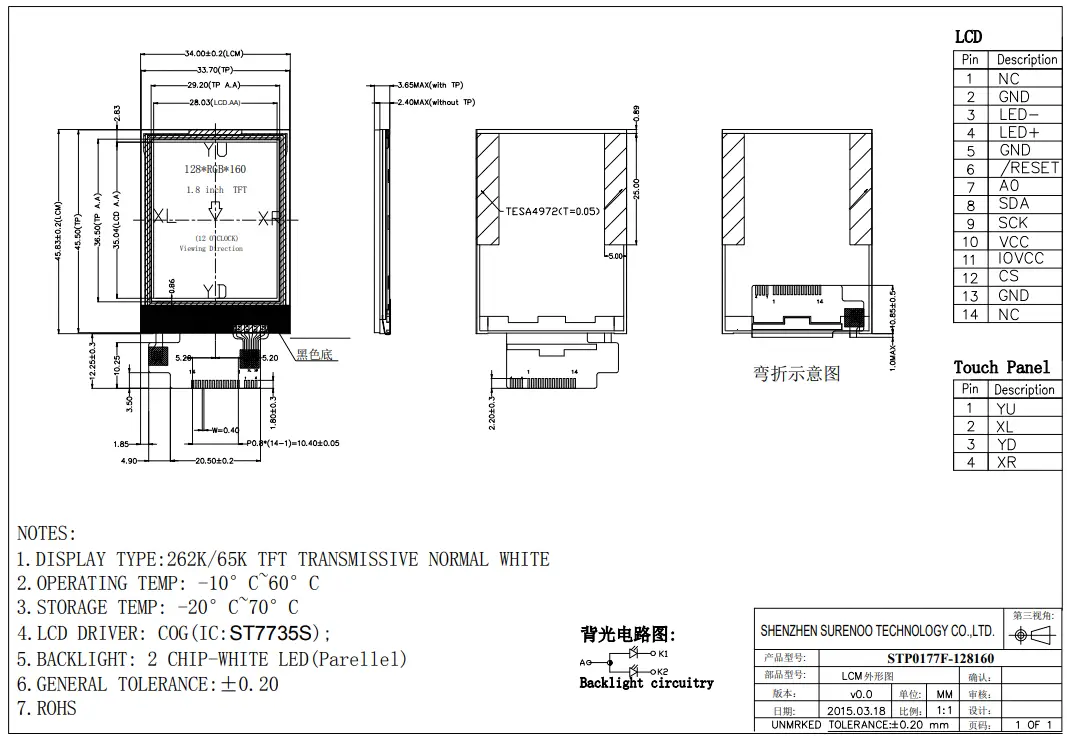
Mechanical Specification
| Item | Specifications | Unit |
| Dimensional outline
| 34.00(W)*45.83(H)*2.40max(T) (FPC not include) | mm |
| Dimensional outline
| 34.00(W)*45.83(H)*3.65max(T) (FPC not include) | mm |
| Resolution
| 128RGB*160 | dots |
| LCD Active area
| 28.03 (W)*35.04 (H) | mm |
| Pixel size
| 0.219(W)*0.219(H) | mm |
Mechanical Dimension
Electrical Maximum Ratings
| Item
| Symbol
| Min
| Max
| Unit
| Note
|
| Supply voltage(IOVCC)
| V | 1.8 | 3.3 | V | |
| Supply voltage(VCC)
| V | 2.8 | 3.3 | V | |
| Operating temperature 工
| TOPR | -20 | 70 | ℃ | |
| Storage temperature
| TSTR | -30 | 80 | ℃ |
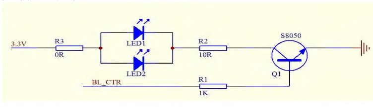
Backlight Characteristic
| Item
| Symbol
| Min
| Typical
| Max
| Unit |
| LED module Forward voltage
| VLED | 2.9 | 3.1 | 3.3 | V |
| LED module current
| ILED | – | 30 | – | mA |
| LCD Surface Luminance
| LS | 150 | 180 | – | Cd/m2 |
| LCM Surface brightness uniform
| LD | 80 | – | – | % |
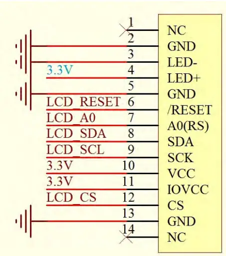
Module Function Description
Display screen
| PIN No.
| Symbol
| Description
| Notes 备注 |
| 1 | NC | No connection
| |
| 2 | GND | Ground
| |
| 3 | LED- | Cathode of Backlight
| |
| 4 | LED+ | Anode of Backlight 2.9-3.3 | |
| 5 | GND | Ground
| |
| 6 | /RESET | LCM Reset pin.Signal is active low
| |
| 7 | A0 | Register select pin) RS=’0’: Display data.(RS=’0’:) RS=’1’: Display data.(RS=’1’: | |
| 8 | SDA | Serial data input / output.
| |
| 9 | SCK | Serial clock pin. ( | |
| 10 | VCC | Power supply for LCM 2.8-3.3V) | |
| 11 | IOVCC | Power supply for LCM 1.8-3.3V) | |
| 12 | CS | Chip select pin (“Low” enable)
| |
| 13 | GND | Ground
| |
| 14 | NC | No connection
|
(Touch panel
| PIN No.
| Symbol
| Description
| Notes
|
| 1 | YU | Touch panel control pin
| |
| 2 | XL | Touch panel control pin
| |
| 3 | YD | Touch panel control pin
| |
| 4 | XR | Touch panel control pin
|
Z180ST029 v0.0
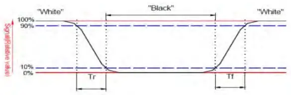
Response time&Contrast ratio
| Item
| Symbol
| Condition
| Remark | Unit
| ||
| Min.
| Typ.
| Max.
| ||||
| Response time
| Tr+Tf | θ=0° | – | 30 | 60 | ms |
| Contrast ratio
| CR | θ=0° | 200 | 300 | – | |
| Item
| Symbol
| Condition
| Remark | Unit
| ||
| Min.
| Typ.
| Max.
| ||||
|
Viewing angle
| Top
| CR≥10
| 20 | 30 | – |
Deg.
|
| Bottom
| CR≥10
| 40 | 45 | – | ||
| Left
| CR≥10
| 40 | 45 | – | ||
| Right
| CR≥10
| 40 | 45 | – | ||
Reliability Trial
| NO.
| ITEM
| CONDITION
| CRITERION
|
| 1 | High Temperature Non-Operating Test | 80℃*120Hrs | No Defect Of |
| Operational | |||
| 2 | Low Temperature Non-Operating Test | -30℃*120Hrs | Function In Room |
| Temperature Are | |||
| 3 | High Temperature/Humidity Non Operating Test | 60℃*90%RH*120Hrs | Allowable |
| 4 | High Temperature Operating Test | 70℃*72Hrs | |
| 5 | Low Temperature Operating Test | -20℃*72Hrs | |
| 6 | Thermal Shock Test | -20 ℃ (30Min) n 70 ℃ | |
| (30Min) *10CYCLES |
inspection standards
Glass defect
| NO | Defect item | Criteria | Remark |
| 1 | Dimension Unconformity (Major defect) | By Engineering Drawing | |
|
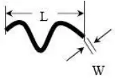
2 | Cracks (Major defect) | 1. Linear cracks panel 【Reject】 2. Nonlinear crack contrast by limited sample | 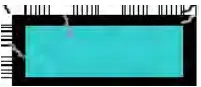 |
|
3 | Glass extrude the conductive area (minor defect) | a: disregards and no influence assemblage. 1) b≤1/3Pin width(non bonding area) 【Accept】 2) bonding area≤0.5mm 【Accept】 | A: Length, b: Width |
|
4 | Pin-side ,conductive area damaged (minor defect) | (a c: disregards) b≤1/3of effective length for bonding electrode 【Accept】 | a: length, b: Width, c: Thickness
|
|
5 | Pin-side,non-conductive area damaged (minor defect) | 1) Damage area don’t touch the ITO (Inclueling contraposition mark, except scribing mark) 【Accept】 2) C<T b≦BM1/3of width | a: Length, b: Width c: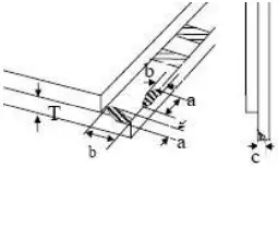 Thickness |
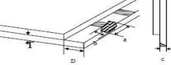
| 【Accept】 3) c=T b not touch the seal glue 【Accept】 4) a disregards | |||
|
6 | Non-pin-side damage (minor defect) | c<T 1)b exceeds 1/3Bm 【Reject】 c=T b not touch the seal glue 【Reject】 | c: Thickness b: width of
damage |
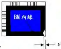
LCD appearance defect(View area)
| NO | Defect item | Criteria | Remark | |
|
1 |
Fiber、glass cratch、polarizer scratch/folded (minor defect) | Specification | Allowable | note1:L: Length, W: Width note2: disregard if out of AA
|
| W≦0.03mm | disregard | |||
| 0.03mm<W≦0.05mm; L≦3.0mm | 2 | |||
| 0.05mm<W≦0.1mm; L≦3.0mm | 1 | |||
| W>0.1mm;L>3.0mm | 0 | |||
|
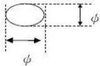
2 | Polarizer bubble、 concave and convex (minor defect) | φ≦0.2mm | disregard | note1: φ=(L+W)/2,L:Length, W :Width note2:disregard if out of AA |
| 0.2mm<φ≦0.3mm | 2 | |||
| 0.3mm<φ≦0.5mm | 1 | |||
| 0.5mm<φ | 0 | |||
|
3 | Black dots、dirty dots、 impurities、eye winker (minor defect) | φ≦0.15mm | disregard | note2:disregard if out of AA
|
| 0.15mm<φ≦0.25mm | 2 | |||
| 0.25mm<φ≦0.3mm | 1 | |||
| 0.3mm<φ | 0 | |||
|
4 | Polarizer prick (minor defect) | φ≦0.1mm | disregard | note1: φ=(L+W)/2,L=Length, W=Width note2:the distance between two dots>5mm |
| 0.1mm<φ≦0.25mm | 3 | |||
| φ>0.25mm | 0 | |||
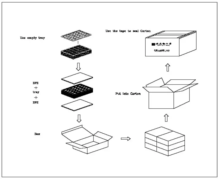
Package Method

Shenzhen Surenoo Technology Co.,Ltd. www.surenoo.com
Skype: Surenoo365


