![]() Model No.: STP0350A3-320480
Model No.: STP0350A3-320480
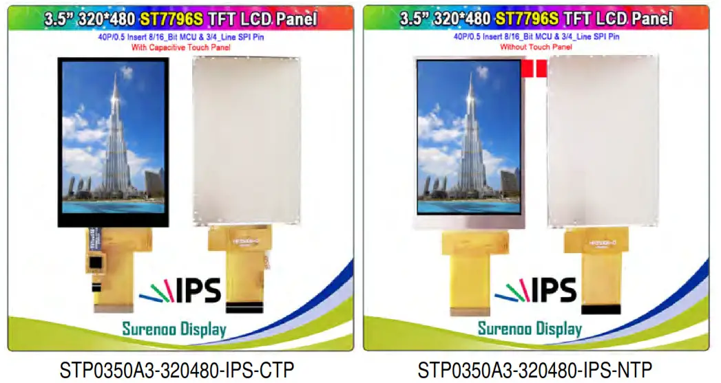
STP0350A3-320480 Series
TFT LCD PANEL USER MANUAL
IPS Mode
STP0350A3-320480 Series TFT LCD Panel
Please dick the following image to buy the sample
 https://www.aliexpress.com/item/4000549728489.html
General Description
| MODEL NO | STP0350A3-320480-IPS |
| Display Mode | Transmissive |
| Display Format | Graphic 320RGB*480 Dot-matrix |
| Input Data | 3 Line-SPT/4 Line-SPI/8bit/16bit interface |
| Viewing Direction | IPS Full View Angle |
| Drive | ST7796S CTP: GT911 |
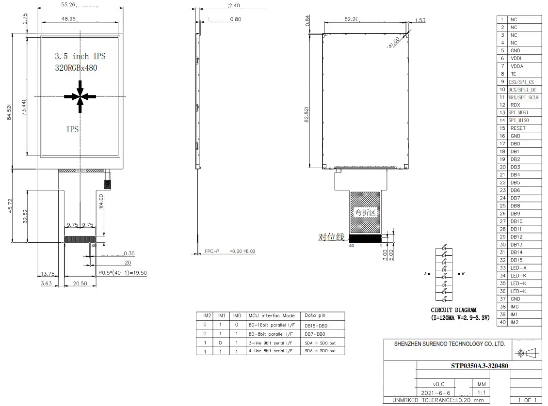
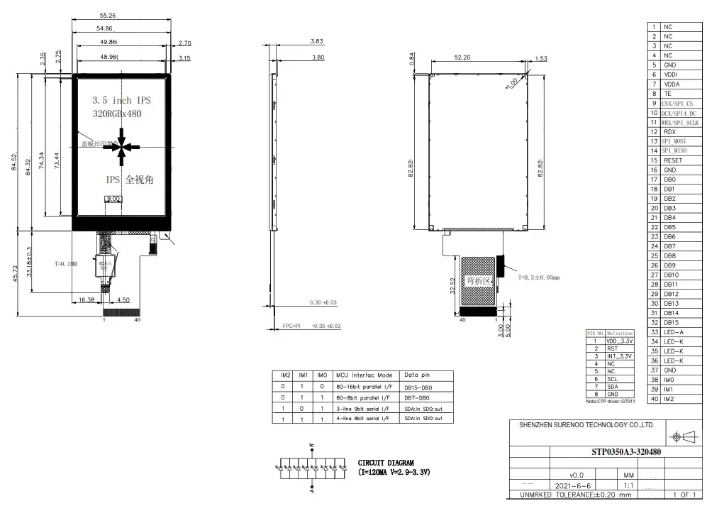
Mechanical Specification
| Item | Specifications | Unit |
| Dimensional outline | CTP: 55.26(W)*84.52(H)*3.83(T) NTP: 55.26(W)*84.52(H)*2.40(T) | mm |
| Resolution | 32ORGB*480 | dots |
| LCD Active area | 48.96(W)*73.44 (H) | mm |
| Pixel size | 0.153(W)*0.153(H) | mm |
Mechanical Dimension (With RTP)
3.1 LCD Panel
NOTES:
- DISPLAY TYPE:TFT
- OPERATING TEMP: -20° C“70° C
- STORAGE TEMP: —30° C“80° C
- 1CD DRIVER: COG(IC:ST7796U);
- BACKLIGHT:
- CHIP-WHITE LED(Paralell)
- GENERAL TOLERANCE: 0. 20
- ROHS
3.2 Touch Screen
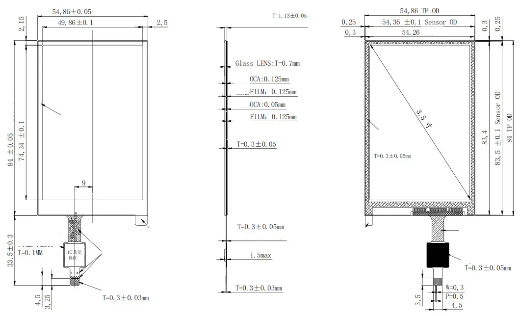
| PIN NO. | Definition |
| 1 | VDD_3.3V |
| 2 | RST |
| 3 | INT_3.3V |
| 4 | NC |
| 5 | NC |
| 6 | SCL |
| 7 | MA |
| 8 | CND |
Note: CTP driver. GT911
| SHENZHEN SURE NO0 TECHNOLOGY CO., LTD. | |||||
| CTP2063A-GFF3.5 | |||||
| UNMRKED TOLERANCE:±0.20 mm | 2021.09.06 | 1 OF 1 | |||
3.3 LCD with Capacitive Touch Screen
NOTES :
- DISPLAY TYPE:TFT
- OPERATING TEMP: -20° C“70° C
- STORAGE TEMP: -30° C780° C
- LCD DRIVER: COG(IC:ST7796U);
- BACKLIGHT: 8 CHIP-WHITE LED(Paralell)
- GENERAL TOLERANCE : +0. 20
- ROHS
Electrical Maximum Ratings
| Item | Symbol | Min | Max | Unit | Note |
| Supply voltage (VDDI) | V | 1.8 | 3.3 | V | – |
| Supply voltage (VDDA) | V | 2.8 | 3.3 | V | – |
| Operating temperature | TOPR | -20 | 70 | °C | – |
| Storage temperature | TSTR | -30 | 80 | °C | – |
Brightness characteristic & Power dissipation
| Item | Symbol | Min | Typical | Max | Unit |
| LED module Forward voltage | VL ED
| 3. | 3. | 3. | V |
| LED module current | km | – | 120 | – | mA |
| LCD Surface Luminance | Ls | 360 | 380 | Cern’ | |
| LCM Surface brightness uniform | LD | 80 | – | – | % |
| LCD power dissipation | PLOD | – | 0.462 | – | W |
NOTE: PLCD-VDD*(I LED+I LCD)
Module Function Description
| PM No. | Symbol | Description | Notes |
| 1 | XL | Touch panel Logical foot | – |
| 2 | YU | Touch panel Logical foot | – |
| 3 | XR | Touch panel Logical foot | – |
| 4 | YD | Touch panel Logical foot | – |
| 5 | GND | Ground | – |
| 6 | VDDI | Power Supply for I/O System. | – |
| 7 | NUM | Power Supply for Analog, Digital System and Booster Circuit. | – |
| 8 | FMARIC(TE) | Tearing effect signal is used to synchronize MCU to frame memory | – |
| 9 | CKUSPICS | -Chip selection pin Low enable. High disable. | – |
| 10 | DCX/RS(SPI-4) | – Display data/command selection pin in MCU interface. DCX=” 1′ : display data or parameter. DCX=. 0′ : command data | – |
| 11 | WILX/SPI SCL | – Write enable in MCU parallel interface. – In SPI mode, this pin is used as SCL. | – |
| 12 | RDX | -Read enable in 8080 MCU parallel interface. -If not used please fix this pin at VDDI or GYP. | – | |||||||||||||||||||||||||
| 13 | SPI SDI/SDA | – SPI interface input pin. – The data is latched on the rising edge of the SCL signal. – If not used, please fix this pin at VDDI or DGND level. | – | |||||||||||||||||||||||||
| 1 I | SPI SDO | -SPI interface output pin. -The data is output on the falling edge of the SCL signal. -If not used let this pin open. | ||||||||||||||||||||||||||
| 15 | RESET | -This signal will reset the device and it must be applied to properly initialize the chip. -Signal is active low. | ||||||||||||||||||||||||||
| 16 | GND | Ground | ||||||||||||||||||||||||||
| 17-24 | DBO-DB7 | MCU parallel interface data bus. | – | |||||||||||||||||||||||||
| 25-32 | DB8-DB15 | MCU parallel interface data bus. | – | |||||||||||||||||||||||||
| 33 | LED-A | Anode of Backlight (2. 9V-3. 3V Typical:3. 1V) | ||||||||||||||||||||||||||
| 34-36 | LED-K | Cathode of Backlight | ||||||||||||||||||||||||||
| 37 | GND | Ground | ||||||||||||||||||||||||||
| 38 | IMO | -The MCU interface mode select. ( MCU
| – | |||||||||||||||||||||||||
| 39 | IM1 | |||||||||||||||||||||||||||
| 40 | 1M2 | – |
6.2 CTP Interface Description
| NO: | Symbol | I/O | DESCRIPTION |
| 1 | YDD | Power supply | CTP Power input |
| 2 | RESET | I | CTP external reset signal, Low is active |
| 3 | INT | 0 | CTP External interrupt to the host |
| 4 | NC | – | No Connection |
| 5 | NC | – | No Connection |
| 6 | SCL | I | C77″ I2C clock input |
| 7 | SDA | I/O | CTP I2C data input and output |
| 8 | GND | Poi ver supply | Poi ver ground |
Response time& Contrast ratio
| Item | Symbol | Condition | Remark | Unit | ||
| Min. | Typ. | Max. | ||||
| Response time | Tr+Tf | 30 | 40 | ms | ||
| Contrast ratio | CR | 0 =0″ | 1000 | – | ||
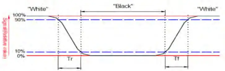
| Contrast ratio (CR)= | Brightness on the “white” state |
| Brightness on the “black” state |
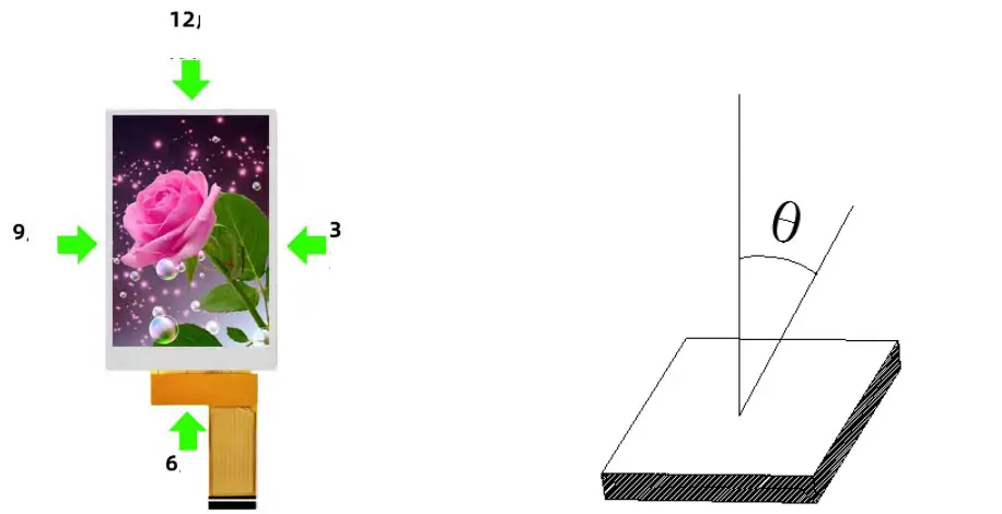
Viewing Angle
| Item | Symbol | Condition | Remark | Unit | ||
| Min. | Typ. | Max. | ||||
| Viewing angle | Top | CR≥10 | 70 | Deg. | ||
| Bottom | CR≥10 | 70 | 80 | – | ||
| Left | CR≥10 | 70 | 80 | – | ||
| Right | CR≥10 | 70 | 80 | – | ||
Reliability Trial
| NO. | ITEM | CONDITION | CRITERION |
| 1 | High Temperature Non-Operating Test | 80°C *120Hrs | No Defect Of Operational Function In Room Temperature Are Allowable |
| -) | Low Temperature Non-Operating Test | -30°C*120Hrs | |
| 3 | High Temperature/Humidity Non Operating Test | 60°C *90%RH*120Hrs | |
| 4 | High Temperature Operating Test | 70°C *72Hrs | |
| 5 | Low Temperature Operating Test | -20°C *72Hrs | |
| 6 | Thermal Shock Test | -20 °C (30Min) v 70 °C (30Min) *10CYCLES |
Inspection standards
10.1Glass defect
| NO | Defect item | Criteria | Remark |
| 1 | Dimension Unconformity (Major defect) | By Engineering Drawing | |
| 2 | Cracks (Major defect) | 1.Linear cracks panel (Reject ] 2.Nonlinear crack contrast by limited sample |  |
| 3 | Glass extrude the conductive area (minor defect) | a: disregards and no influence assemblage. 1) b‘.1/3Pin width(non bonding area) (Accept ] 2)bonding area‘.0. 5mm (Accept] | A: Length, b: Width |
| 4 | Pin-side ,conductive area damaged (minor defect) | (a c: disregards) b*.c1/3of effective length for bonding electrode (Accept] | a: length, b: Width, c: Thickness 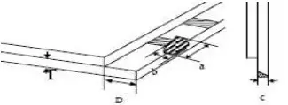 |
| 5 | Pin-side,non-conductive area damaged (minor defect) | 1)Damage area don’t touch the ITO (Including contraposition mark, except scribing mark) [Accept] 2)C<T b —– BM 1/3of width [Accept] 3)c=T b not touch the seal glue [Accept] 4)a disregards | a: Length, b: Width c: Thickness |
| 6 | Non-pin-side damage (minor defect) | c<T 1)b exceeds 1/3Bm [Reject ]
c=T b not touch the seal glue [Reject] | c: Thickness b: width of damage 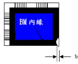 |
2LCD appearance defect(View area)
| NO | Defect item | Criteria | Remark | |
| 1 | Fiber, glass cratch, polarizer scratch/folded (minor defect) | Specification | Allowable | notel : L: Length, W: Width note2: disregard if out of AA 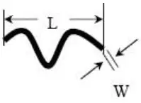 |
| Wg0 03 mm | disregard | |||
| 0.03mm<W g O. 05mm; L g 3. Omm | 2 | |||
| 0.05mm<W g0. 1mm; L ‘.– 3. Omni | 1 | |||
| W>0.1mm;L>3.0min | 0 | |||
| N | Polarizer bubble, concave and convex (minor defect) | 4) g 0.2mm | disregard | notel: 4) = (L+W) /2, L :Length, W :Width note2:disregard if out of AA 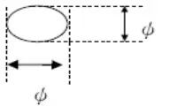 |
| 0.2mm< 4) g O. 3mm | 2 | |||
| 0.3mm< 4) g 0. 5mm | 1 | |||
| 0 5mm< 4) | 0 | |||
| 3 | Black dots, dirty dots, impurities, eye winker (minor defect) | 4) g 0.15mm | disregard | note2:disregard if out of AA |
| 0.15mm< 4) g 0. 25mm | 2 | |||
| 0.25mm< 4) g 0. 3mm | 1 | |||
| 0 3mm< 4) | 0 | |||
| 4 | Polarizes prick (minor defect) | 4) g 0.1mm | disregard | notel: 4) = (L+W) /2, L=Length, W=Width note2:the distance between two dots>5nun |
| 0.1mm<4 ‘ 0. 25mm | 3 | |||
| 4) >O. 25mm | 0 | |||
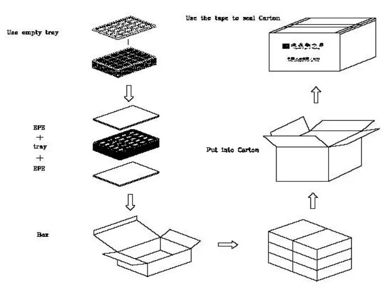
Package Method
![]()
 MECARD:TEL:0086-17820607849;URL:
http://www.surenoo.com
EMAIL:[email protected]
N:Potter Hao; ORG: Surenoo Technology;
https://wa.me/qr/4GGOIDYZ2PXXN1
http://qr.kakao.com/talk/THom9tzJN5OMzvx1vTL1V.LvnEc-
https://line.me/ti/p/oas8BmVLVd
Shenzhen Surenoo Technology Co.,Ltd.
www.surenoo.com
Skype: Surenoo365
Reference Controller Datasheet
TFT LCD Panel Selection Guide
ST7796S
GT911


