STP0350B1-320480 Series TFT LCD Display Screen Panel
Product Information: STP0350B1-320480(TN) TFT LCD PANEL
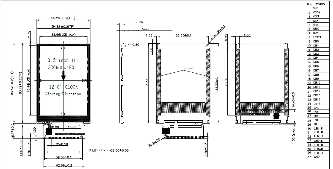
The STP0350B1-320480(TN) series TFT LCD panel is manufactured by Shenzhen Surenoo Technology Co., Ltd. The panel has a display format of graphic 320RGB*480 dot-matrix 320xRGBx480 with a transmissive display mode and 8bit/16bit interface input data. It is equipped with the ILI9488 drive and CTP: GT911 touch panel driver. The LCD panel measures 3.5 inches and has a viewing direction of 12 o’clock.
Mechanical Specification
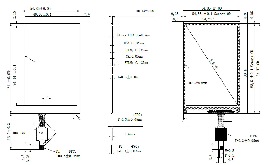
The LCD panel has an active area of 48.96(W)*73.44 (H) mm with a resolution of 320RGB*480 dots. The pixel size is 0.153(W)*0.153(H) mm. The CTP has a dimensional outline of 55.26(W)*84.52(H)*4.13(T) mm, while the RTP has a dimensional outline of 55.26(W)*84.52(H)*4.00(T) mm, and the NTP has a dimensional outline of 55.26(W)*84.52(H)*2.70(T) mm.
Module Function Description
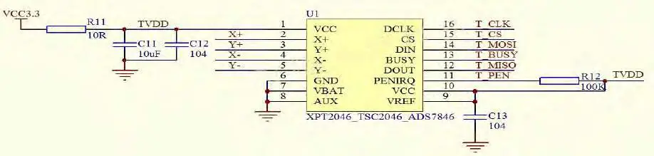
The TFT LCD PANEL has 26 pins, including GND, VDDA, VDDI, CSX, DCX, WRX, RDX, RESET, DB0-DB7, and DB8-DB15.
Electrical Maximum Ratings
The minimum and maximum supply voltage for VDDI is 1.8V and 3.3V, respectively, while the minimum and maximum supply voltage for VDDA is 2.8V and 3.3V, respectively. The operating temperature range is -20°C to 70°C, while the storage temperature range is -30°C to 80°C.
Brightness Characteristic & Power Dissipation
The LED module forward voltage has a minimum of 29V and a typical value of 3.1V with a maximum of 3.3V. The LED module current has no minimum value, a typical value of 128mA, and no maximum value. The LCD surface luminance has a typical value of 300 cd/m2, while the LCM surface brightness uniformity has a typical value of 0.39%. The LCD power dissipation varies depending on the voltage and current, with PLCD = VDD * (ILED+ILCD).
Product Usage Instructions
The STP0350B1-320480(TN) TFT LCD PANEL is commonly used in various electronic devices, including but not limited to smartphones, tablets, laptops, and other display devices. Before using the product, ensure that the device’s power supply voltage is within the specified range of 1.8V to 3.3V for VDDI and 2.8V to 3.3V for VDDA.
The LCD panel can be connected to the device using an 8bit or 16bit interface input data. The panel is equipped with the ILI9488 drive and CTP: GT911 touch panel driver. The touch panel driver can be used to provide touch functionality to the display device.
The LCD panel has 26 pins, including GND, VDDA, VDDI, CSX, DCX, WRX, RDX, RESET, DB0-DB7, and DB8-DB15. The pins can be connected to the device’s circuit board using the corresponding pin definitions.
When using the LCD panel, ensure that the operating temperature range is within -20°C to 70°C, while the storage temperature range is within -30°C to 80°C. The brightness and power dissipation values should also be considered when designing the device that will use the LCD panel.
General Description
| MODEL NO | STP0350B1-320480(TN) |
| Display Mode | Transmissive |
| Display Format | Graphic 320RGB*480 Dot-matrix 320xRGBx480 |
| Input Data | 8bit/16bit interface |
| Viewing Direction | 12 o’clock 12 |
| Drive | ILI9488 CTP: GT911 |
Mechanical Specification
| Item | Specifications | Unit |
| Dimensional outline | CTP: 55.26(W)*84.52(H)*4.13(T) RTP: 55.26(W)*84.52(H)*4.00(T) NTP: 55.26(W)*84.52(H)*2.70(T) | mm |
| Resolution | 320RGB*480 | dots |
| LCD Active area | 48.96(W)*73.44 (H) | mm |
| Pixel size | 0.153(W)*0.153(H) | mm |
Mechanical Dimension
NOTES:
- DISPLAY TYPE:TFT
- OPERATING TEMP: -20°C~70°C
- STORAGE TEMP: -30°C~80°C
- LCD DRIVER: COG(IC:ILI9488);
- BACKLIGHT: 8 CHIP-WHITE LED (Parallels)
- GENERAL TOLERANCE:±0.20
- ROHS

Mechanical Dimension (CTP)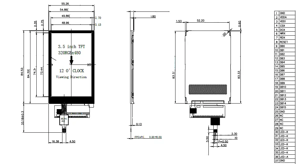
NOTES:
- DISPLAY TYPE:TFT
- OPERATING TEMP: -20°C~70°C
- STORAGE TEMP: -30°C~80°C
- LCD DRIVER: COG(IC:ILI9488);
- BACKLIGHT: 8 CHIP-WHITE LED (Parellel)
- GENERAL TOLERANCE:±0.20
- ROHS
NOTES
- Glass +Film +Film
- GT911
- ≥85%
- ≥6H
- -20℃~+70℃ ≤90%RH
- -30℃~+80℃ ≤90%RH
- I2C :COF
- 3.3V :3.3V
- ±0.15
Electrical Maximum Ratings
| Item | Symbol | Min | Max | Unit | Note |
| Supply voltage (VDDI) | V | 1.8 | 3.3 | V | – |
| Supply voltage (VDDA) | V | 2.8 | 3.3 | V | – |
| Operating temperature | TOPR | -20 | 70 | ℃ | – |
| Storage temperature | TSTR | -30 | 80 | ℃ | – |
NOTE: VDDI (2.8V~3.3V)。
Brightness characteristic & Power dissipation
| Item | Symbol | Min | Typical | Max | Unit |
| LED module Forward voltage | VLED | 2.9 | 3.1 | 3.3 | V |
| LED module current | ILED | – | 128 | – | mA |
| LCD Surface Luminance | LS | 280 | 300 | – | Cd/m2 |
| LCM Surface brightness uniform | LD | 80 | – | – | % |
| LCD power dissipation | PLCD | – | 0.39 | – | W |
NOTE: PLCD=VDD * (ILED+ILCD)
Module Function Description
| PIN No. | Symbol | Description | Notes |
| 1 | GND | Ground | – |
| 2 | VDDA | Power Supply for Analog, Digital System and Booster Circuit.(2.8-3.3V) | – |
| 3 | VDDI | Power Supply for I/O System.(1.8-3.3V) | – |
| 4 | CSX |
High disable. | – |
| 5 | DCX |
|
– |
| 6 | WRX |
| – |
| 7 | RDX |
| – |
| 8 | RESET |
| – |
| 9-16 | DB0-DB7 | MCU parallel interface data bus. | – |
| 17-24 | DB8-DB15 | MCU parallel interface data bus. | – |
| 25 | GND | Ground | – |
| 26 | YD | Touch panel Logical foot | – |
| 27 | XR | Touch panel Logical foot | – |
| 28 | YU | Touch panel Logical foot | – |
| 29 | XL | Touch panel Logical foot | – |
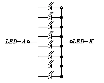
| 30 | LED-K1 | Cathode of Backlight | – |
| 31 | LED-K2 | Cathode of Backlight | – |
| 32 | LED-K3 | Cathode of Backlight | – |
| 33 | LED-K4 | Cathode of Backlight | – |
| 34 | LED-K5 | Cathode of Backlight | – |
| 35 | LED-K6 | Cathode of Backlight | – |
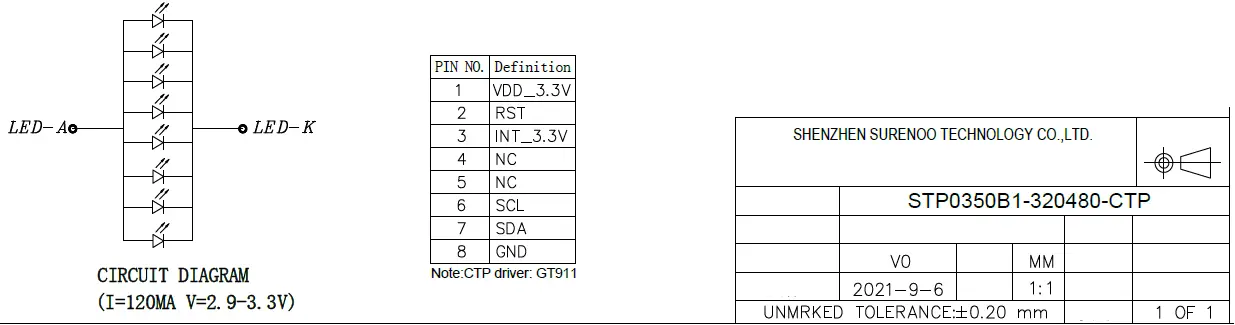
| 36 | LED-A | Anode of Backlight (2.9V-3.3V Typical:3.1V)(:3.1V) | – |
| 37 | GND | Ground | – |
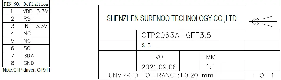
CTP Interface Description
| NO. | Symbol | I/O | DESCRIPTION |
| 1 | VDD | Power supply | CTP Power input |
| 2 | RESET | I | CTP external reset signal, Low is active |
| 3 | INT | O | CTP External interrupt to the host |
| 4 | NC | – | No Connection |
| 5 | NC | – | No Connection |
| 6 | SCL | I | CTP I2C clock input |
| 7 | SDA | I/O | CTP I2C data input and output |
| 8 | GND | Power supply | Power ground |
STP0350B-16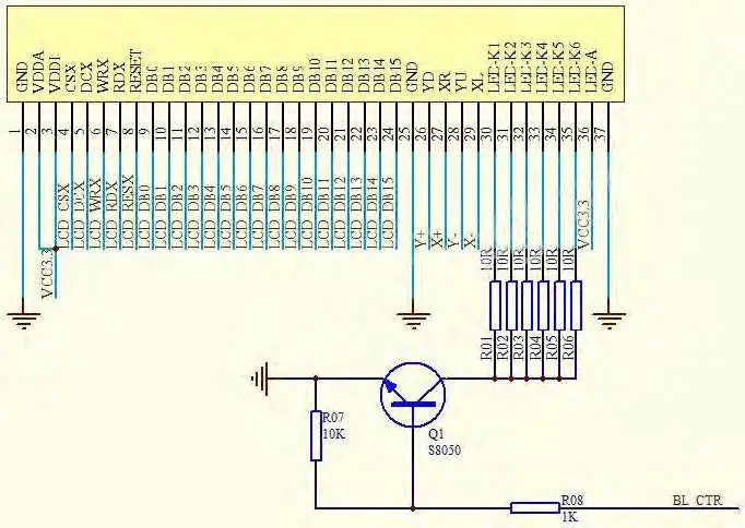
STP0350B-8 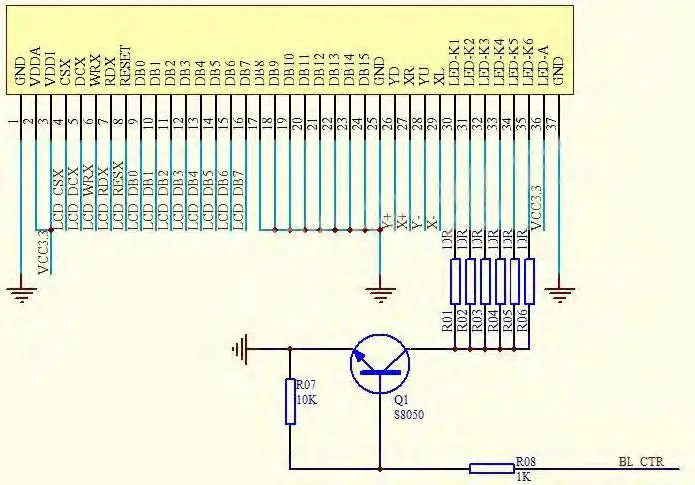
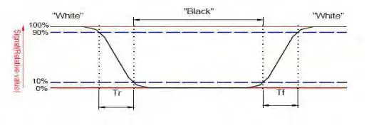
Response time & Contrast ratio
| Item | Symbol | Condition | Remark | Unit | ||
| Min. | Typ. | Max. | ||||
| Response time | Tr+Tf | θ=0° | – | 20 | 40 | ms |
| Contrast ratio | CR | θ=0° | – | 500 | – | – |
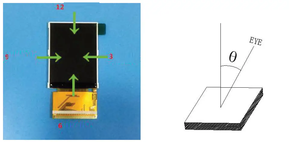
Viewing Angle
| Item | Symbol | Condition | Remark | Unit | ||
| Min. | Typ. | Max. | ||||
| Viewing angle | Top 12 | CR≥10 | 50 | 60 | – | Deg. |
| Bottom 6 | CR≥10 | 50 | 60 | – | ||
| Left 9 | CR≥10 | 60 | 70 | – | ||
| Right 3 | CR≥10 | 60 | 70 | – | ||
Reliability Trial
| NO. | ITEM | CONDITION | CRITERION |
| 1 | High Temperature Non-Operating Test | 80℃*120Hrs | No Defect Of |
| Operational | |||
| 2 | Low Temperature Non-Operating Test | -30℃*120Hrs | Function In Room |
| Temperature Are | |||
| 3 | High Temperature/Humidity Non Operating Test | 60℃*90%RH*120Hrs | Allowable |
| 4 | High Temperature Operating Test | 70℃*72Hrs | |
| 5 | Low Temperature Operating Test | -20℃*72Hrs | |
| 6 | Thermal Shock Test | -20 ℃ (30Min) n 70 ℃ | |
| (30Min) *10CYCLES |
Inspection standards
Glass defect
| NO | Defect item | Criteria | Remark |
| 1 | Dimension Unconformity (Major defect) | By Engineering Drawing | |
| 2 | Cracks (Major defect) |
|  |
| 3 | Glass extrude the conductive area (minor defect) | a: disregards and no influence assemblage.
| A: Length, b: Width |
| 4 | Pin-side ,conductive area damaged (minor defect) | (a c: disregards) b≤1/3of effective length for bonding electrode 【Accept】 | a: length, b: Width, c: Thickness
|
| 5 | Pin-side,non-conductive area damaged (minor defect) | 1)Damage area don’t touch the ITO ( Including contraposition mark, except scribing mark 【Accept】 | a: Length, b: Width c: Thickness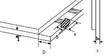 |
| 2) C<T b≦BM1/3of width 【Accept】 3) c=T | 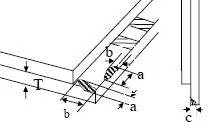 | ||
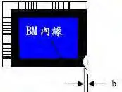
| 6 | Non-pin-side damage (minor defect) | c<T 1)b exceeds 1/3Bm 【Reject】 c=T b not touch the seal glue【Reject】 | c: Thickness b: width of damage |
LCD appearance defect(View area)
| NO | Defect item | Criteria | Remark | |
| 1 | Fiber, glass cratch, polarizer scratch/folded (minor defect) | Specification | Allowable | note1:L: Length, W: Width note2: disregard if out of AA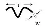
|
| W≦0.03mm | disregard | |||
| 0.03mm<W≦0.05mm; L≦3.0mm | 2 | |||
| 0.05mm<W≦0.1mm; L≦3.0mm | 1 | |||
| W>0.1mm;L>3.0mm | 0 | |||
| 2 | Polarizer bubble, concave and convex (minor defect) | φ≦0.2mm | disregard | Note1: φ=(L+W)/2,L:Length, W :Width Note2: disregard if out of AA |
| 0.2mm<φ≦0.3mm | 2 | |||
| 0.3mm<φ≦0.5mm | 1 | |||
| 0.5mm<φ | 0 | |||
| 3 | Black dots, dirty dots, impurities, eye winker (minor defect) | φ≦0.15mm | disregard | note2:disregard if out of AA
|
| 0.15mm<φ≦0.25mm | 2 | |||
| 0.25mm<φ≦0.3mm | 1 | |||
| 0.3mm<φ | 0 | |||
| 4 | Polarizer prick (minor defect) | φ≦0.1mm | disregard | Note1: φ=(L+W)/2,L=Length, W=Width Note2:the distance between two dots>5mm |
| 0.1mm<φ≦0.25mm | 3 | |||
| φ>0.25mm | 0 | |||
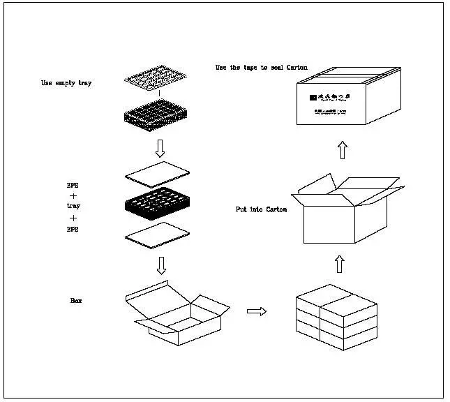
Package Method