VISHAY IRFI9Z14GPBF Power MOSFET Owner’s Manual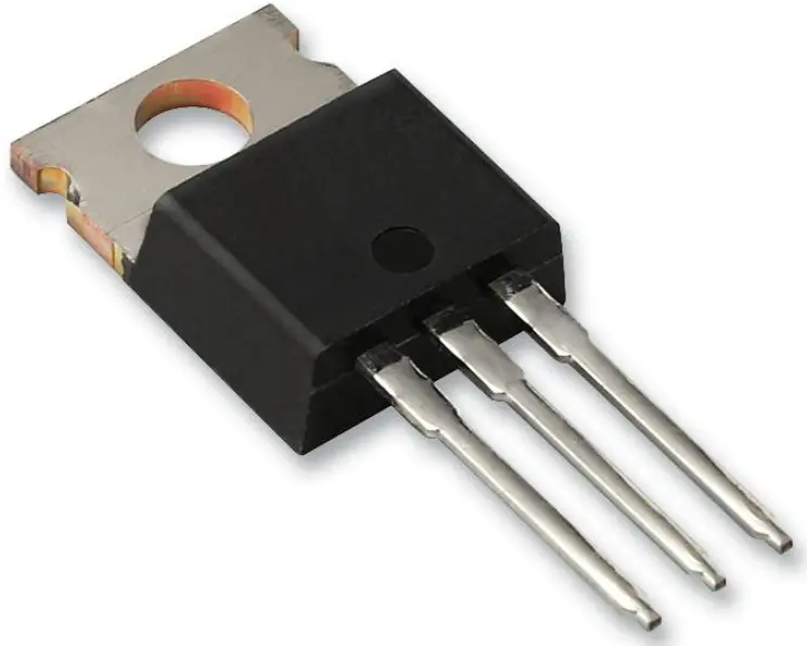
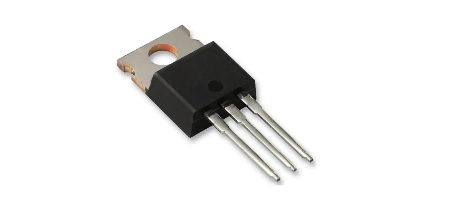
TO-220 FULLPAK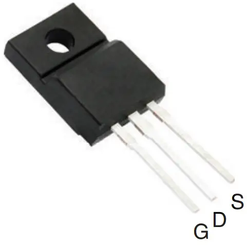
P-Channel MOSFET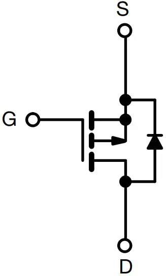
| PRODUCT SUMMARY | ||
| VDS (V) | -60 | |
| RDS(on) (W) | VGS = -10 V | 0.50 |
| Qg (Max.) (nC) | 12 | |
| Qgs (nC) | 3.8 | |
| Qgd (nC) | 5.1 | |
| Configuration | Single | |
FEATURES
- Isolated package
- High voltage isolation = 2.5 kVRMS (t = 60 s; f = 60 Hz)
- Sink to lead creepage distance = 4.8 mm
- P-channel
- 175 °C operating temperature
- Dynamic dV/dt rating
- Low thermal resistance
- Material categorization: for definitions of compliance please see www.vishay.com/doc?99912
DESCRIPTION
Third generation power MOSFETs from Vishay provide the designer with the best combination of fast switching, ruggedized device design, low on-resistance and cost-effectiveness. The TO-220 FULLPAK eliminates the need for additional insulating hardware in commercial-industrial applications. The molding compound used provides a high isolation capability and a low thermal resistance between the tab and external heatsink. This isolation is equivalent to using a 100 micron mica barrier with standard TO-220 product. The FULLPAK is mounted to a heatsink using a single clip or by a single screw fixing.
| ORDERING INFORMATION | |
| Package | TO-220 FULLPAK |
| Lead (Pb)-free | IRFI9Z14GPbF |
| ABSOLUTE MAXIMUM RATINGS TC = 25 °C, unless otherwise noted | |||||
| PARAMETER | SYMBOL | LIMIT | UNIT | ||
| Drain-source voltage | VDS | -60 | V | ||
| Gate-source voltage | VGS | ± 20 | |||
| Continuous drain current | VGS at -10 V | TC = 25 °C | ID | -5.3 | A |
| TC = 100 °C | -3.8 | ||||
| Pulsed drain current a | IDM | -21 | |||
| Linear derating factor | 0.18 | W/°C | |||
| Single pulse avalanche energy b | EAS | 120 | mJ | ||
| Repetitive avalanche current a | IAR | -5.3 | A | ||
| Repetitive avalanche energy a | EAR | 2.7 | mJ | ||
| Maximum power dissipation | TC = 25 °C | PD | 27 | W | |
| Peak diode recovery dV/dt c | dV/dt | -4.5 | V/ns | ||
| Operating junction and storage temperature range | TJ, Tstg | -55 to +175 | °C | ||
| Soldering recommendations (peak temperature) d | For 10 s | 300 | |||
| Mounting torque | M3 screw | 0.6 | Nm | ||
Notes
a. Repetitive rating; pulse width limited by maximum junction temperature (see fig. 11)
b. VDD = -25 V, starting TJ = 25 °C, L = 5.0 mH, RG = 25 , IAS = -5.3 A (see fig. 12)
c. ISD -6.7 A, dI/dt 90 A/μs, VDD VDS, TJ 175 °C
d. 1.6 mm from case
| THERMAL RESISTANCE RATINGS | ||||
| PARAMETER | SYMBOL | TYP. | MAX. | UNIT |
| Maximum junction-to-ambient | RthJA | – | 65 | °C/W |
| Maximum junction-to-case (drain) | RthJC | – | 5.5 | |
| SPECIFICATIONS TJ = 25 °C, unless otherwise noted | |||||||
| PARAMETER | SYMBOL | TEST CONDITIONS | MIN. | TYP. | MAX. | UNIT | |
| Static | |||||||
| Drain-ssource breakdown voltage | VDS | VGS = 0 V, ID = -250 μA | -60 | – | – | V | |
| VDS temperature coefficient | DVDS/TJ | Reference to 25 °C, ID = -1 mA | – | -0.060 | – | V/°C | |
| Gate-source threshold voltage | VGS(th) | VDS = VGS, ID = -250 μA | -2.0 | – | -4.0 | V | |
| Gate-source leakage | IGSS | VGS = ± 20 V | – | – | ± 100 | nA | |
| Zero gate voltage drain current | IDSS | VDS = -60 V, VGS = 0 V | – | – | -100 | μA | |
| VDS = -48 VGS = 0 V, TJ = 150 °C | – | – | -500 | ||||
| Drain-source on-state resistance | RDS(on) | VGS = -10 V | ID = -3.2 A b | – | – | 0.50 | W |
| Forward transconductance | gfs | VDS = -25 V, ID = -3.2 A b | 1.6 | – | – | S | |
| Dynamic | |||||||
| Input capacitance | Ciss | VGS = 0 V, VDS = -25 V,f = 1.0 MHz, see fig. 5 | – | 270 | – | pF | |
| Output capacitance | Coss | – | 170 | – | |||
| Reverse transfer capacitance | Crss | – | 31 | – | |||
| Drain to sink capacitance | C | f = 1.0 MHz | – | 12 | – | ||
| Total gate charge | Qg | VGS = -10 V | ID = -6.7 A, VDS = -48 V,see fig. 6 and 13 b | – | – | 12 | nC |
| Gate-source charge | Qgs | – | – | 3.8 | |||
| Gate-drain charge | Qgd | – | – | 5.1 | |||
| Turn-on delay time | td(on) | VDD = -30 V, ID = -6.7 A, RG = 24 W, RD= 4.0 W,see fig. 10b | – | 11 | – | ns | |
| Rise time | tr | – | 63 | – | |||
| Turn-off delay time | td(off) | – | 9.6 | – | |||
| Fall time | tf | – | 31 | – | |||
| Internal drain inductance | LD | Between lead, D6 mm (0.25″) from package and center ofGdie contactS | – | 4.5 | – | nH | |
| Internal source inductance | LS | – | 7.5 | – | |||
| Drain-Source Body Diode Characteristics | |||||||
| Continuous source-drain diode current | IS | MOSFET symbolDshowing theintegral reverseGp – n junction diodeS | – | – | -5.3 | A | |
| Pulsed diode forward current a | ISM | – | – | -21 | |||
| Body diode voltage | VSD | TJ = 25 °C, IS = -5.3 A, VGS = 0 V b | – | – | -5.5 | V | |
| Body diode reverse recovery time | trr | TJ = 25 °C, IF = -6.7 A, dI/dt = 100 A/μs b | – | 80 | 160 | ns | |
| Body diode reverse recovery charge | Qrr | – | 0.096 | 0.19 | μC | ||
| Forward turn-on time | ton | Intrinsic turn-on time is negligible (turn-on is dominated by LS and LD) | |||||
Notes
a. Repetitive rating; pulse width limited by maximum junction temperature (see fig. 11)
b. Pulse width 300 μs; duty cycle 2 %
TYPICAL CHARACTERISTICS 25 °C, unless otherwise noted
Fig. 1 – Typical Output Characteristics, TC= 25 °C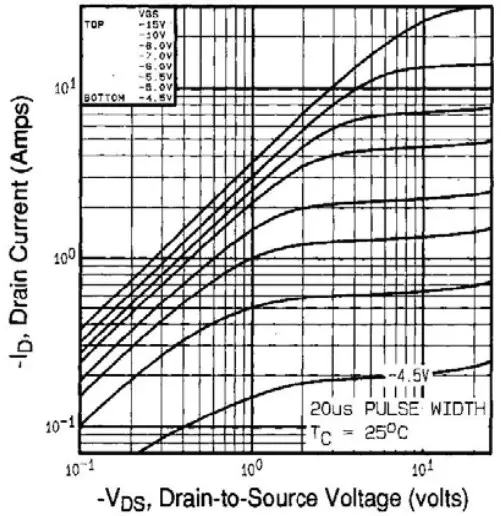
Fig. 2 – Typical Output Characteristics, TC= 175 °C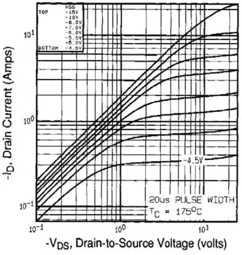
Fig. 3 – Typical Transfer Characteristics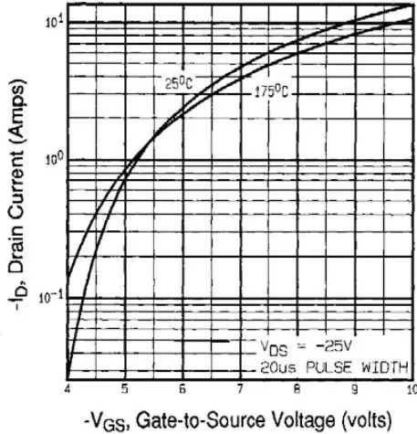
Fig. 4 – Normalized On-Resistance vs. Temperature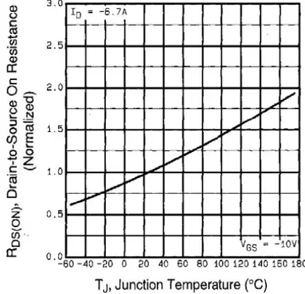
Fig. 5 – Typical Capacitance vs. Drain-to-Source Voltage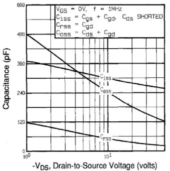
Fig. 6 – Typical Gate Charge vs. Gate-to-Source Voltage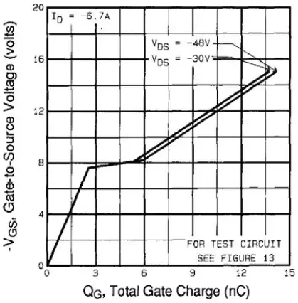
Fig. 7 – Typical Source-Drain Diode Forward Voltage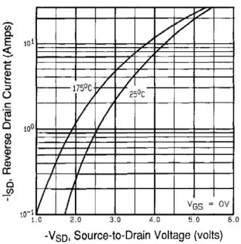
Fig. 8 – Maximum Safe Operating Area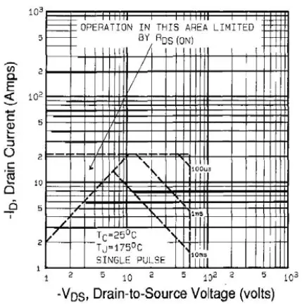
Fig. 9 – Maximum Drain Current vs. Case Temperature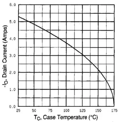
Fig. 10a – Switching Time Test Circuit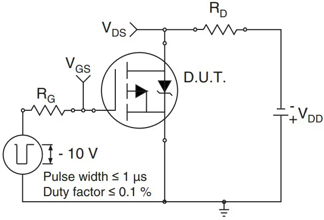
Fig. 10b – Switching Time Waveforms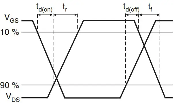
Fig. 11 – Maximum Effective Transient Thermal Impedance, Junction-to-Case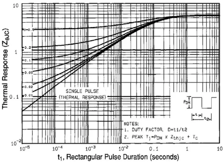
Fig. 12a – Unclamped Inductive Test Circuit Fig.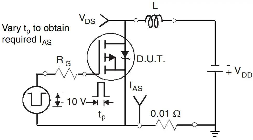
12b – Unclamped Inductive Waveforms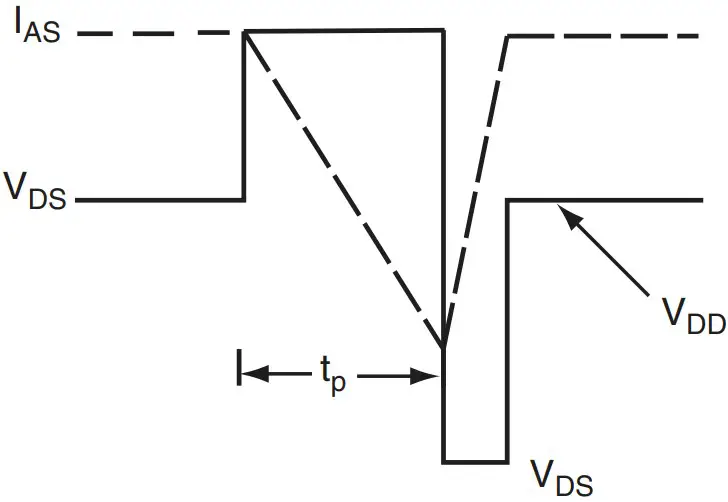
Fig. 12c – Maximum Avalanche Energy vs. Drain Current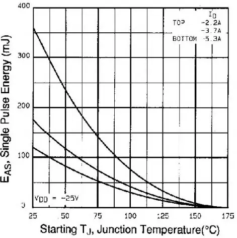
Fig. 13a – Basic Gate Charge Waveform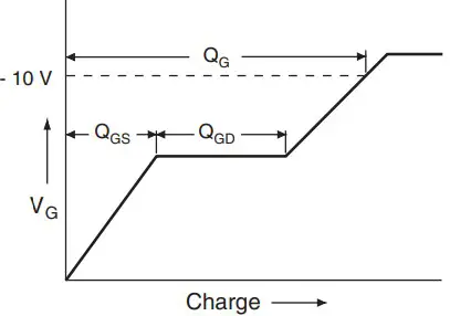
Fig. 13b – Gate Charge Test Circuit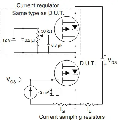
Peak Diode Recovery dV/dt Test Circuit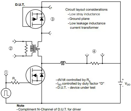
Note
- Compliment N-Channel of D.U.T. for driver
Fig. 14 – For P-Channel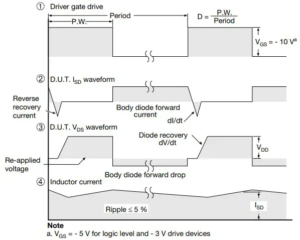
TO-220 FULLPAK (High Voltage)
OPTION 1: FACILITY CODE = 9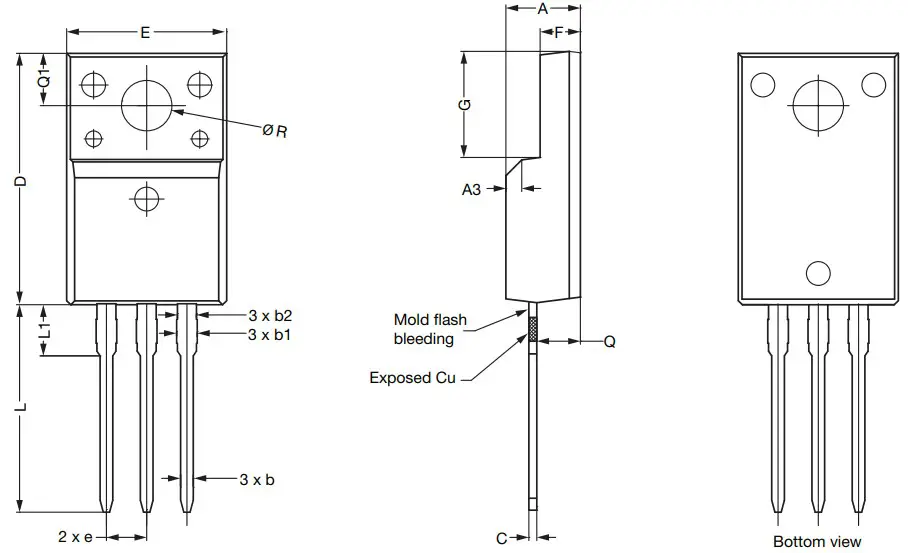
| MILLIMETERS | |||
| DIM. | MIN. | NOM. | MAX. |
| A | 4.60 | 4.70 | 4.80 |
| b | 0.70 | 0.80 | 0.91 |
| b1 | 1.20 | 1.30 | 1.47 |
| b2 | 1.10 | 1.20 | 1.30 |
| C | 0.45 | 0.50 | 0.63 |
| D | 15.80 | 15.87 | 15.97 |
| e | 2.54 BSC | ||
| E | 10.00 | 10.10 | 10.30 |
| F | 2.44 | 2.54 | 2.64 |
| G | 6.50 | 6.70 | 6.90 |
| L | 12.90 | 13.10 | 13.30 |
| L1 | 3.13 | 3.23 | 3.33 |
| Q | 2.65 | 2.75 | 2.85 |
| Q1 | 3.20 | 3.30 | 3.40 |
| Ø R | 3.08 | 3.18 | 3.28Notes |
- To be used only for process drawing
- These dimensions apply to all TO-220 FULLPAK leadframe versions 3 leads
- All critical dimensions should C meet Cpk > 1.33
- All dimensions include burrs and plating thickness
- No chipping or package damage
- Facility code will be the 1st character located at the 2nd row of the unit marking
OPTION 2: FACILITY CODE = Y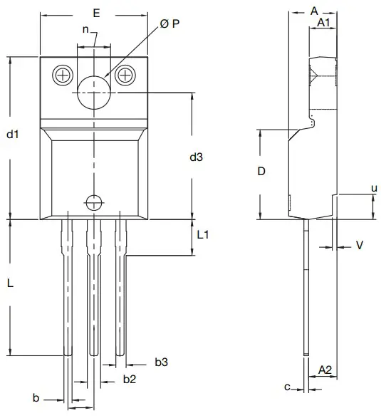
| MILLIMETERS | INCHES | |||
| DIM. | MIN. | MAX. | MIN. | MAX. |
| A | 4.570 | 4.830 | 0.180 | 0.190 |
| A1 | 2.570 | 2.830 | 0.101 | 0.111 |
| A2 | 2.510 | 2.850 | 0.099 | 0.112 |
| b | 0.622 | 0.890 | 0.024 | 0.035 |
| b2 | 1.229 | 1.400 | 0.048 | 0.055 |
| b3 | 1.229 | 1.400 | 0.048 | 0.055 |
| c | 0.440 | 0.629 | 0.017 | 0.025 |
| D | 8.650 | 9.800 | 0.341 | 0.386 |
| d1 | 15.88 | 16.120 | 0.622 | 0.635 |
| d3 | 12.300 | 12.920 | 0.484 | 0.509 |
| E | 10.360 | 10.630 | 0.408 | 0.419 |
| e | 2.54 BSC | 0.100 BSC | ||
| L | 13.200 | 13.730 | 0.520 | 0.541 |
| L1 | 3.100 | 3.500 | 0.122 | 0.138 |
| n | 6.050 | 6.150 | 0.238 | 0.242 |
| Ø P | 3.050 | 3.450 | 0.120 | 0.136 |
| u | 2.400 | 2.500 | 0.094 | 0.098 |
| V | 0.400 | 0.500 | 0.016 | 0.020 |
| ECN: E19-0180-Rev. D, 08-Apr-2019 DWG: 5972 | ||||
Notes
- To be used only for process drawing
- These dimensions apply to all TO-220 FULLPAK leadframe versions 3 leads
- All critical dimensions should C meet Cpk > 1.33
- All dimensions include burrs and plating thickness
- No chipping or package damage
- Facility code will be the 1st character located at the 2nd row of the unit marking
Disclaimer
ALL PRODUCT, PRODUCT SPECIFICATIONS AND DATA ARE SUBJECT TO CHANGE WITHOUT NOTICE TO IMPROVE RELIABILITY, FUNCTION OR DESIGN OR OTHERWISE.
Vishay Intertechnology, Inc., its affiliates, agents, and employees, and all persons acting on its or their behalf (collectively,
“Vishay”), disclaim any and all liability for any errors, inaccuracies or incompleteness contained in any datasheet or in any other disclosure relating to any product.
Vishay makes no warranty, representation or guarantee regarding the suitability of the products for any particular purpose or the continuing production of any product. To the maximum extent permitted by applicable law, Vishay disclaims (i) any and allliability arising out of the application or use of any product, (ii) any and all liability, including without limitation special, consequential or incidental damages, and (iii) any and all implied warranties, including warranties of fitness for particular purpose, non-infringement and merchantability.
Statements regarding the suitability of products for certain types of applications are based on Vishay’s knowledge of typical requirements that are often placed on Vishay products in generic applications. Such statements are not binding statements about the suitability of products for a particular application. It is the customer’s responsibility to validate that a particular product with the properties described in the product specification is suitable for use in a particular application. Parameters provided in datasheets and / or specifications may vary in different applications and performance may vary over time. All operating parameters, including typical parameters, must be validated for each customer application by the customer’s technical experts.
Product specifications do not expand or otherwise modify Vishay’s terms and conditions of purchase,including but not limited to the warranty expressed therein. Hyperlinks included in this datasheet may direct users to third-party websites. These links are provided as a convenience and for informational purposes only. Inclusion of these hyperlinks does not constitute an endorsement or an approval by Vishay of any of the products, services or opinions of the corporation, organization or individual associated with the third-party website. Vishay disclaims any and all liability and bears no responsibility for the accuracy, legality or content of the third-party website or for that of subsequent links.
Except as expressly indicated in writing, Vishay products are not designed for use in medical, life-saving, or life-sustaining applications or for any other application in which the failure of the Vishay product could result in personal injury or death.
Customers using or selling Vishay products not expressly indicated for use in such applications do so at their own risk. Please contact authorized Vishay personnel to obtain written terms and conditions regarding products designed for such applications.
No license, express or implied, by estoppel or otherwise, to any intellectual property rights is granted by this document or by any conduct of Vishay. Product names and markings noted herein may be trademarks of their respective owners.


