onsemi Secondary Side Regulated Isolated Flyback Converter
SPECIFICATION
Devices | Applications | Input Voltage | Output Power | Topology | Board Size |
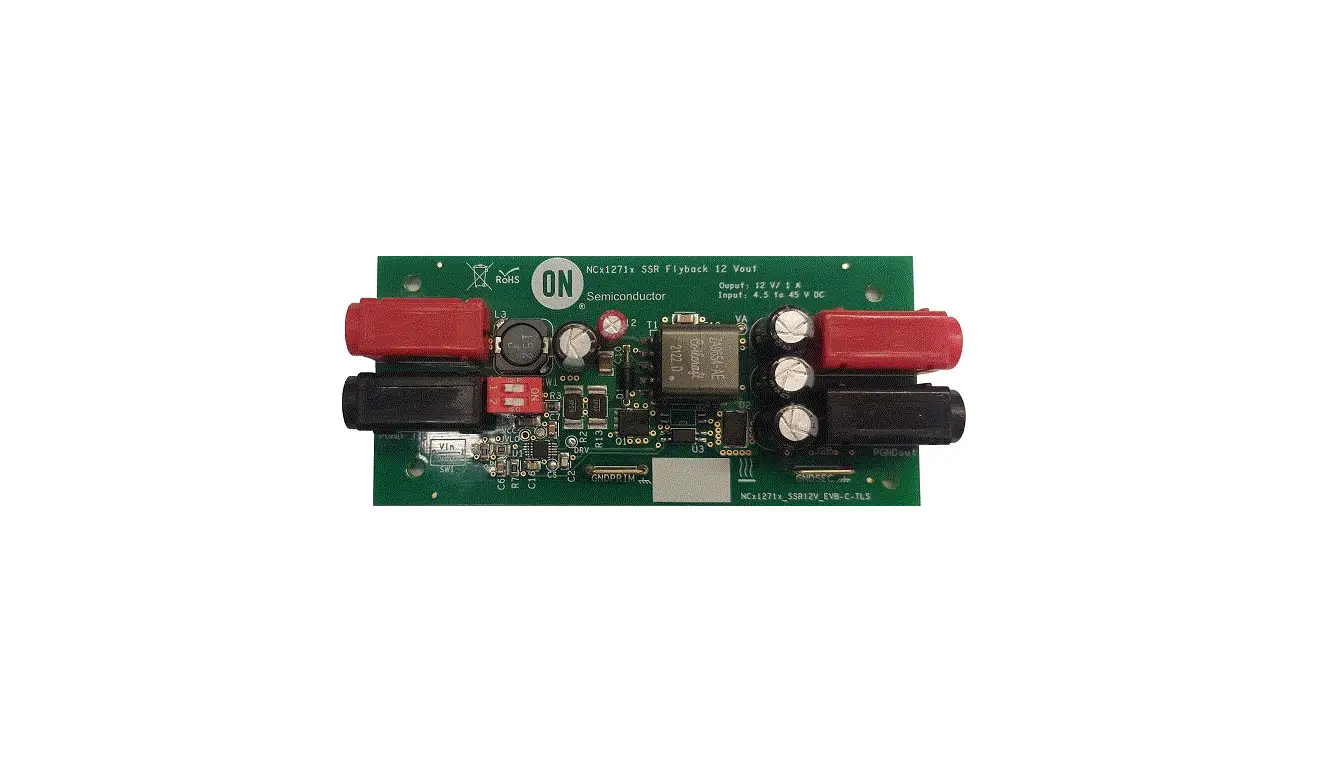
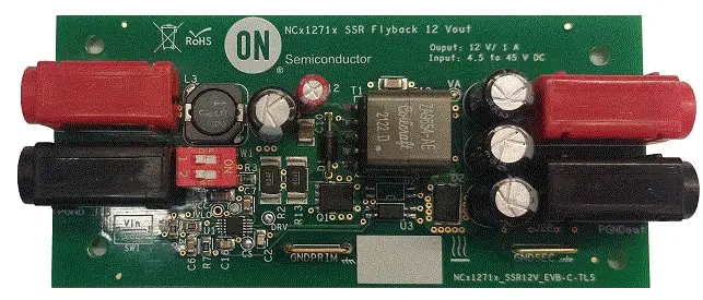
| NCV12711 | Automotive | 4 − 45 V dc | 12 W | Current−Mode Flyback | 100 x 47 x 15 mm |
| Output Spec | Turn on Time | Efficiency | Operating Temperature | Cooling | Standby Power |
| 12 V/1 A | < 100 ms | Peaks to 89 % @ full load | 0 – 50°C | Open Frame in Still Air | See the tables on page 8 |
DESCRIPTION
This evaluation board user’s manual provides elementary information about a secondary side regulated flyback converter NCV12711SSRGEVB built with the NCV12711 operated in current−mode control at 100 kHz. This control circuit offers many features to build an energy−efficient converter with all the needed protections like cycle−by−cycle current limit with a 250−mV sense voltage, over−current protection (OCP) and over−voltage protection (OVP) on the VCC pin. The controller drives an N−channel MOSFET as with any classical flyback converter at a user−adjustable switching frequency. The secondary side hosts a low−Vf diode for efficient rectification in continuous conduction mode (CCM).
The primary−side section drives a transformer whose primary inductance is 8 H. The current is sensed via two paralleled 40−m resistors which limit the maximum output current to a safe value in fault condition. The board is rated to 12 W of continuous output power in free air at the lowest input voltage. This level is delivered down to a 4.5−V input. The converter is able to deliver output power up to 4−V input, which is the turn−off level adjusted by an UVLO resistor divider. At higher input voltages, the board may deliver more power but thermal runaway may happen and the board temperature must be monitored.
The regulation is ensured directly on secondary side requiring the use of an optocoupler. The advantage of this solution is better output voltage regulation in comparison with Primary−Side−Regulated converter.
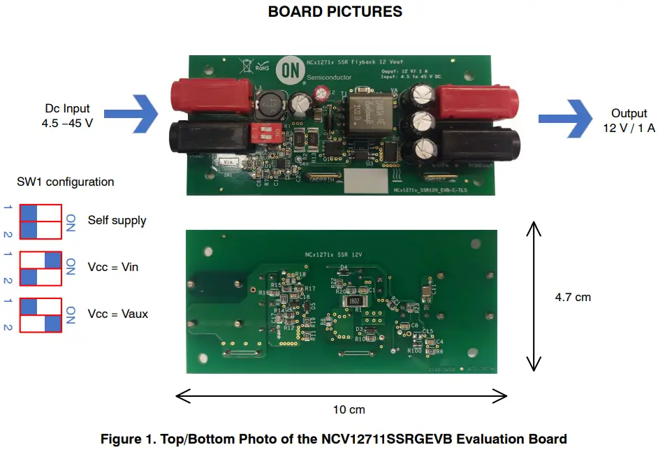
The switch SW1 let you select different configurations to test the circuit:
- a is closed, b open: in this mode, the VCC and VIN pin are connected together while the auxiliary winding is not used. The maximum input voltage is 25 V; going beyond this value will trip the OVP on VCC pin.
- b is closed, a open: in this mode, the controller is supplied by the VIN pin only during start−up sequence and VCC is biased by the rectified auxiliary supply. The input voltage can go up to 45 V.
- a and b are open: the controller is self−supplied via internal LDO and the auxiliary winding is not used. The input voltage can go up to 45 V.
Due to secondary side regulation, the switch SW1 affects only the efficiency of the system. For more details, see the Efficiency and Standby data in TEST DATA section. The internal operational amplifier coupled to external components ensures the realization of a type 2 compensator. Using the simulation model or a bench measurement, components values were adjusted to crossover above 1 kHz.
The maximum crossover is limited by the right−half−plane−zero (RHPZ) which degrades the phase response at the lowest input voltage and the largest output current. The board is equipped with two connectors letting you easily connect the network analyzers probes for a convenient measurement. The collected graphs show a comfortable phase margin at crossover.
A simple front−end filter limits the amount of parasitic noise going back to the source and it must be properly damped to avoid interaction with the downstream converter. C9 is providing that function with its equivalent series\ resistance (ESR).
KEY FEATURES OF NCV12711
- Internal 20−mA current source for lossless start−up sequence and self−supply operation
- Smooth start−up sequence with frequency sweep
- Internal operational amplifier with precise 2.5−V reference voltage
- Current−mode control operation
- Short circuit protection
- Over voltage protection
- Input Voltage UVLO with Hysteresis
- Shutdown threshold for external disable
- 0% duty ratio mode for low standby power
- Single Resistor Programmable Oscillator
- User−Adjustable Soft−Start Ramp

EVALUATION BOARD SCHEMATIC DIAGRAM
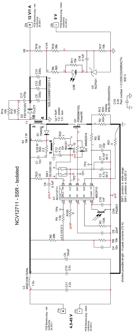
Figure 2. Schematic of the NCV12711SSRGEVB Evaluation Board
MAGNETICS DATA
ZA9654−AE from Coilcraft:
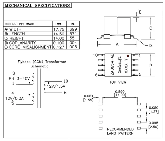
Figure 3. Mechanical Specifications
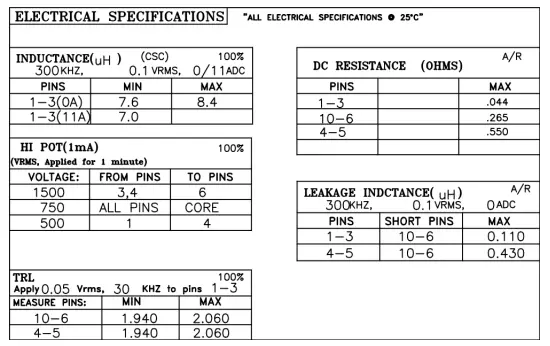
Figure 4. Electrical Specifications
TEST DATA
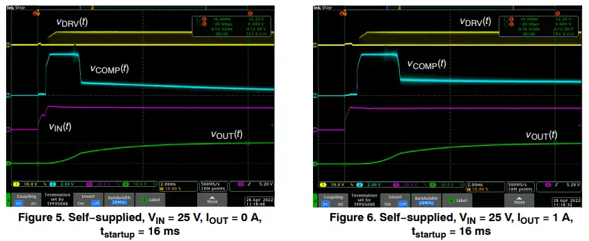
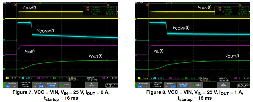
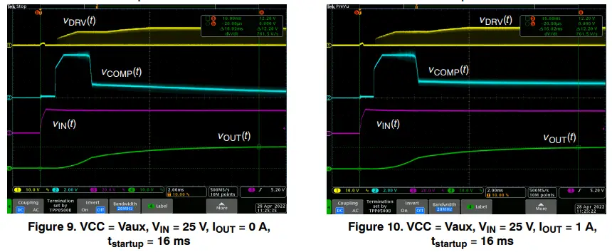
Startup Time
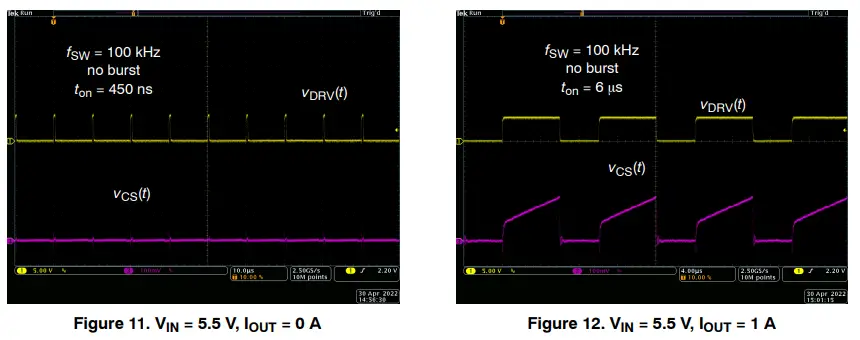
Steady−state Operation
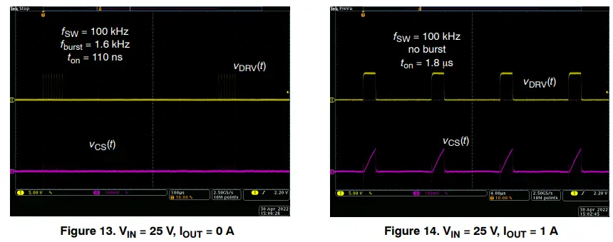

Load Transient Response
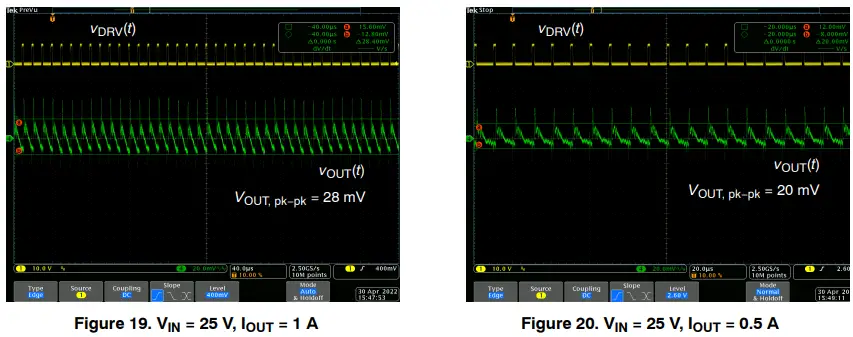
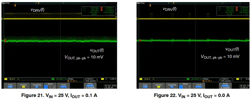
Output Voltage Ripple
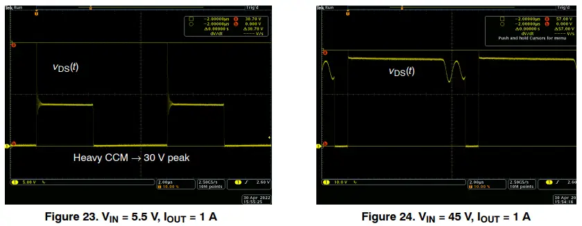
Drain−Source Voltage
Standby Data
Table 1. NO−LOAD INPUT POWER WHEN THE IC IS SELF−SUPLIED VIA LDO
VIN (V) | IIN (mA) | PIN (mW) | VOUT (V) |
4.5 | 10.9 | 49.0 | 12.1 |
| 15 | 6.0 | 89.5 | 12.1 |
25 | 4.2 | 106.0 | 12.1 |
| 45 | 3.6 | 164.3 | 12.1 |
Table 2. NO−LOAD INPUT POWER WHEN THE VCC PIN IS CONNECTED TO VIN PIN
| VIN (V) | IIN (mA) | PIN (mW) | VOUT (V) |
4.5 | 11.2 | 50.6 | 12.1 |
| 15 | 6.0 | 90.0 | 12.1 |
25 | 4.3 | 106.5 | 12.1 |
Table 3. NO−LOAD INPUT POWER WHEN THE VCC PIN IS CONNECTED TO AUX WINDING
VIN (V) | IIN (mA) | PIN (mW) | VOUT (V) |
4.5 | 24.7 | 111.3 | 12.1 |
| 15 | 10.5 | 156.5 | 12.1 |
25 | 5.0 | 125.5 | 12.1 |
| 45 | 2.8 | 125.1 | 12.1 |
Efficiency Data
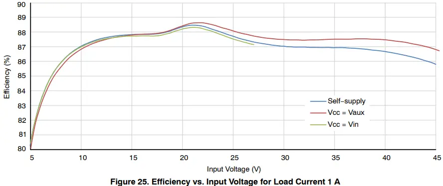
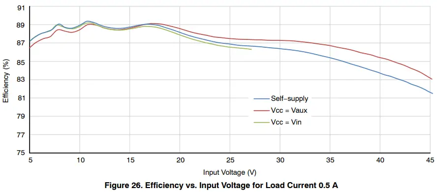
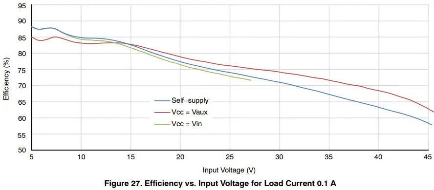
Table 4. BILL OF MATERIALS
Designator | Qty | Description | Value | Tolerance | Footprint | Manufacturer | Manufacturer Part Number |
C1 | 1 | Ceramic capacitor | 10 nF/100 V | 20% | 0805 | Generic | |
| C2 | 1 | Ceramic capacitor | 22 pF/10 V | 20% | 0805 | Generic | |
C3 | 1 | Ceramic capacitor | 4.7 µF/50 V | 10% | 1206 | TDK | CGA5L3X7R1H475K160AB |
| C4 | 1 | Ceramic capacitor | 10 nF/10 V | 10% | 0805 | Generic | |
C5, C13, C14 | 3 | Electrolytic capacitor | 330 µF/16 V | 20% | TH | Rubycon | 16ZLG330MEFC8X11.5 |
| C6 | 1 | Ceramic capacitor | 22 nF/10 V | 10% | 0805 | Generic | |
C7, C8, C18 | 3 | Ceramic capacitor | 0.1 µF/50 V | 10% | 0805 | Generic | |
| C9 | 1 | Electrolytic capacitor | 100 µF/50 V | 20% | TH | Rubycon | 50ZL100MEFC8X11.5 |
C10, C11 | 2 | Ceramic capacitor | 2.2 µF/100 V | 10% | 1210 | Kemet | C1210C225M1RACTU |
| C12 | 1 | Electrolytic capacitor | 4.7 µF/25 V | 20% | TH | Generic | |
C15 | 0 | Ceramic capacitor | NU | − | 0805 | Generic | |
| C16 | 1 | Ceramic capacitor | 1 nF/16 V | 10% | 0805 | Generic | |
C17 | 1 | Ceramic capacitor | 470 pF/100 V | 10% | 0805 | Generic | |
| C19 | 1 | Ceramic capacitor | 3.3 nF/630 V | 10% | 1206 | Kemet | C1206C332KBRACTU |
D1 | 1 | HV diode | 1N4937 | − | DO−41 | onsemi | 1N4937G |
| D2 | 1 | Power diode | FSV10120V | − | TO−277 | onsemi | FSV10120V |
D3 | 1 | Signal diode | MMSD914 | − | SOD−123 | onsemi | |
| D4 | 1 | Signal diode | BAV21 | − | SOD−123 | onsemi | |
D5 | 0 | Zener diode 12 V | NU | − | SOD−123 | onsemi | MMSZ4699T1G |
| J1a, J2a | 2 | Banana plug | − | − | multicomp | 24.243.1 | |
J1b, J2b | 2 | Banana plug | − | − | multicomp | 24.243.2 | |
| L3 | 1 | Inductor | 1.5 µH | 30% | Coilcraft | MSS1038−152NL | |
R1 | 1 | Resistor | 18 kQ | 1% | 2512 | Generic | |
| R2, R13 | 2 | Resistor | 40 mQ | 1% | 2512 | Vishay | WSL2512R0400FEA |
R3 | 1 | Resistor | 845 Q | 1% | 0805 | Generic | |
| R4 | 1 | Resistor | 1.5 kQ | 1% | 0805 | Generic | |
R5 | 1 | Resistor | 68 kQ | 1% | 0805 | Generic | |
| R6, R11, R17 | 3 | Resistor | 10 kQ | 1% | 0805 | Generic | |
R7 | 1 | Resistor | 133 kQ | 1% | 0805 | Generic | |
| R8, R18, R19 | 0 | Resistor | NU | 1% | 0805 | Generic | |
R9 | 1 | Resistor | 560 Q | 1% | 0805 | Generic | |
| R10, R16 | 2 | Resistor | 10 Q | 1% | 0805 | Generic | |
R12, R14 | 2 | Resistor | 100 Q/0.5 W | 1% | 0805 | Generic | |
| R15 | 1 | Resistor | 38 Q | 1% | 0805 | Generic | |
R20 | 1 | Resistor | 2.2 Q | 1% | 0805 | Generic | |
| R21, R100 | 2 | Resistor | 0 Q | 1% | 0805 | Generic | |
R22 | 1 | Resistor | 1 Q | 1% | 0805 | Generic | |
| R23 | 1 | Resistor | 33 Q | 1% | 0805 | Generic | |
SW1 | 1 | PCB Switch | − | multicomp | MCNDS−02V | ||
| T1 | 1 | Transformer | ZA9654−AE | − | Coilcraft | ZA9654−AE | |
Q1 | 1 | N−Channel MOSFET | FDMS86103L | − | PQFN−8 | onsemi | FDMS86103L |
U1 | 1 | PWM controller | NCV12711 | − | MSOP−10 | onsemi | NCV12711A |
| U2 | 0 | Optocoupler | NU | − | SSOP−4 | Renesas | |
U3 | 1 | Optocoupler | PS2801C−1 | − | SSOP−4 | Renesas | |
U4 | 1 | Shunt Regulator | NCP431 | − | SOT−23 | onsemi | NCP431 |
onsemi, , and other names, marks, and brands are registered and/or common law trademarks of Semiconductor Components Industries, LLC dba “onsemi” or its affiliates and/or subsidiaries in the United States and/or other countries. onsemi owns the rights to a number of patents, trademarks, copyrights, trade secrets, and other intellectual property. A listing of onsemi’s product/patent coverage may be accessed at www.onsemi.com/site/pdf/Patent−Marking.pdf. onsemi is an Equal Opportunity/Affirmative Action Employer. This literature is subject to all applicable copyright laws and is not for resale in any manner.
The evaluation board/kit (research and development board/kit) (hereinafter the “board”) is not a finished product and is not available for sale to consumers. The board is only intended for research, development, demonstration and evaluation purposes and will only be used in laboratory/development areas by persons with an engineering/technical training and familiar with the risks associated with handling electrical/mechanical components, systems and subsystems. This person assumes full responsibility/liability for proper and safe handling. Any other use, resale or redistribution for any other purpose is strictly prohibited.
THE BOARD IS PROVIDED BY ONSEMI TO YOU “AS IS” AND WITHOUT ANY REPRESENTATIONS OR WARRANTIES WHATSOEVER. WITHOUT LIMITING THE FOREGOING, ONSEMI (AND ITS LICENSORS/SUPPLIERS) HEREBY DISCLAIMS ANY AND ALL REPRESENTATIONS AND WARRANTIES IN RELATION TO THE BOARD, ANY MODIFICATIONS, OR THIS AGREEMENT, WHETHER EXPRESS, IMPLIED, STATUTORY OR OTHERWISE, INCLUDING WITHOUT LIMITATION ANY AND ALL REPRESENTATIONS AND WARRANTIES OF MERCHANTABILITY, FITNESS FOR A PARTICULAR PURPOSE, TITLE, NON−INFRINGEMENT, AND THOSE ARISING FROM A COURSE OF DEALING, TRADE USAGE, TRADE CUSTOM OR TRADE PRACTICE.
onsemi reserves the right to make changes without further notice to any board.
You are responsible for determining whether the board will be suitable for your intended use or application or will achieve your intended results. Prior to using or distributing any systems that have been evaluated, designed or tested using the board, you agree to test and validate your design to confirm the functionality for your application. Any technical, applications or design information or advice, quality characterization, reliability data or other services provided by onsemi shall not constitute any representation or warranty by onsemi, and no additional obligations or liabilities shall arise from onsemi having provided such information or services.
onsemi products including the boards are not designed, intended, or authorized for use in life support systems, or any FDA Class 3 medical devices or medical devices with a similar or equivalent classification in a foreign jurisdiction, or any devices intended for implantation in the human body. You agree to indemnify, defend and hold harmless onsemi, its directors, officers, employees, representatives, agents, subsidiaries, affiliates, distributors, and assigns, against any and all liabilities, losses, costs, damages, judgments, and expenses, arising out of any claim, demand, investigation, lawsuit, regulatory action or cause of action arising out of or associated with any unauthorized use, even if such claim alleges that onsemi was negligent regarding the design or manufacture of any products and/or the board.
This evaluation board/kit does not fall within the scope of the European Union directives regarding electromagnetic compatibility, restricted substances (RoHS), recycling (WEEE), FCC, CE or UL, and may not meet the technical requirements of these or other related directives.
FCC WARNING – This evaluation board/kit is intended for use for engineering development, demonstration, or evaluation purposes only and is not considered by onsemi to be a finished end product fit for general consumer use. It may generate, use, or radiate radio frequency energy and has not been tested for compliance with the limits of computing devices pursuant to part 15 of FCC rules, which are designed to provide reasonable protection against radio frequency interference. Operation of this equipment may cause interference with radio communications, in which case the user shall be responsible, at its expense, to take whatever measures may be required to correct this interference.
onsemi does not convey any license under its patent rights nor the rights of others.
LIMITATIONS OF LIABILITY: onsemi shall not be liable for any special, consequential, incidental, indirect or punitive damages, including, but not limited to the costs of requalification, delay, loss of profits or goodwill, arising out of or in connection with the board, even if onsemi is advised of the possibility of such damages. In no event shall onsemi’s aggregate liability from any obligation arising out of or in connection with the board, under any theory of liability, exceed the purchase price paid for the board, if any.
The board is provided to you subject to the license and other terms per onsemi’s standard terms and conditions of sale. For more information and documentation, please visit www.onsemi.com
Customer Support
TECHNICAL PUBLICATIONS:
Technical Library: www.onsemi.com/design/resources/technical−documentation
onsemi Website: www.onsemi.com
ONLINE SUPPORT:
www.onsemi.com/support
For additional information, please contact your local Sales Representative at
www.onsemi.com/support/sales