![]() MCP1661 Isolated Flyback Converter
MCP1661 Isolated Flyback Converter
MCP1661
Isolated Flyback Converter
Reference Design
Instructions
MCP1661 Isolated Flyback Converter
Note the following details of the code protection feature on Microchip products:
- Microchip products meet the specifications contained in their particular Microchip Data Sheet.
- Microchip believes that its family of products is secure when used in the intended manner, within operating specifications, and under normal conditions.
- Microchip values and aggressively protects its intellectual property rights. Attempts to breach the code protection features of Microchip product is strictly prohibited and may violate the Digital Millennium Copyright Act.
- Neither Microchip nor any other semiconductor manufacturer can guarantee the security of its code. Code protection does not mean that we are guaranteeing the product is “unbreakable” Code protection is constantly evolving. Microchip is committed to continuously improving the code protection features of our products.
This publication and the information herein may be used only with Microchip products, including to design, test, and integrate Microchip products with your application. Use f this information in any other manner violates these terms. Information regarding device applications is provided only for your convenience and may be superseded by updates. It is your responsibility to ensure that your application meets with your specifications. Contact your local Microchip sales office for additional support or, obtain additional support at https://www.microchip.com/en-us/support/design-help/client-supportservices.
THIS INFORMATION IS PROVIDED BY MICROCHIP “AS IS”. MICROCHIP MAKES NO REPRESENTATIONS OR WARRANTIES OF ANY KIND WHETHER EXPRESS OR IMPLIED, WRITTEN OR ORAL, STATUTORY OR OTHERWISE, RELATED TO THE INFORMATION INCLUDING BUT NOT LIMITED TO ANY IMPLIED WARRANTIES OF NONINFRINGEMENT, MERCHANTABILITY, AND FITNESS FOR A PARTICULAR PURPOSE, OR WARRANTIES RELATED TO ITS CONDITION, QUALITY, OR PERFORMANCE. IN NO EVENT WILL MICROCHIP BE LIABLE FOR ANY INDIRECT, SPECIAL, PUNITIVE, INCIDENTAL, OR CONSEQUENTIAL LOSS, DAMAGE, COST, OR EXPENSE OF ANY KIND WHATSOEVER RELATED TO THE INFORMATION OR ITS USE, HOWEVER CAUSED, EVEN IF MICROCHIP HAS BEEN ADVISED OF THE POSSIBILITY OR THE DAMAGES ARE FORESEEABLE.
TO THE FULLEST EXTENT ALLOWED BY LAW, MICROCHIP’S TOTAL LIABILITY ON ALL CLAIMS IN ANY WAY RELATED TO THE INFORMATION OR ITS USE WILL NOT EXCEED THE AMOUNT OF FEES, IF ANY, THAT YOU HAVE PAID DIRECTLY TO MICROCHIP FOR THE INFORMATION. Use of Microchip devices in life support and/or safety applications is entirely at the buyer’s risk, and the buyer agrees to defend, indemnify and hold harmless Microchip from any and all damages, claims, suits, or expenses resulting from such use. No licenses are conveyed, implicitly or otherwise, under any Microchip intellectual property rights unless otherwise stated.
Trademarks
The Microchip name and logo, the Microchip logo, Adaptec, AVR, AVR logo, AVR Freaks, BesTime, BitCloud, CryptoMemory, CryptoRF, dsPIC, flexPWR, HELDO, IGLOO, JukeBlox, KeeLoq, Kleer, LANCheck, LinkMD, maXStylus, maXTouch, MediaLB, megaAVR, Microsemi, Microsemi logo, MOST, MOST logo, MPLAB, OptoLyzer, PIC, picoPower, PICSTART, PIC32 logo, PolarFire, Prochip Designer, QTouch, SAM-BA, SenGenuity, SpyNIC, SST, SST Logo, SuperFlash, Symmetricom, SyncServer, Tachyon, TimeSource, tinyAVR, UNI/O, Vectron, and XMEGA are registered trademarks of Microchip Technology Incorporated in the U.S.A. and other countries.
AgileSwitch, APT, ClockWorks, The Embedded Control Solutions Company, EtherSynch, Flashtec, Hyper Speed Control, HyperLight Load, Libero, motorBench, mTouch, Powermite 3, Precision Edge, ProASIC, ProASIC Plus, ProASIC Plus logo, Quiet- Wire, SmartFusion, SyncWorld, Temux, TimeCesium, TimeHub, TimePictra, TimeProvider, TrueTime, and ZL are registered trademarks of Microchip Technology Incorporated in the U.S.A.
Adjacent Key Suppression, AKS, Analog-for-the-Digital Age, Any Capacitor, AnyIn, AnyOut, Augmented Switching, BlueSky, BodyCom, Clockstudio, CodeGuard, CryptoAuthentication, CryptoAutomotive, CryptoCompanion, CryptoController, dsPICDEM, dsPICDEM.net, Dynamic Average Matching, DAM, ECAN, Espresso T1S, EtherGREEN, GridTime, IdealBridge, InCircuit Serial Programming, ICSP, INICnet, Intelligent Paralleling, IntelliMOS, Inter-Chip Connectivity, JitterBlocker, Knob-on-Display, KoD, maxCrypto, maxView, memBrain, Mindi, MiWi, MPASM, MPF, MPLAB Certified logo, MPLIB, MPLINK, MultiTRAK, NetDetach, Omniscient Code Generation, PICDEM, PICDEM.net, PICkit, PICtail, PowerSmart, PureSilicon, QMatrix, REAL ICE, Ripple Blocker, RTAX, RTG4, SAM-ICE, Serial Quad I/O, simpleMAP, SimpliPHY, SmartBuffer, SmartHLS, SMART-I.S., storClad, SQI, SuperSwitcher, SuperSwitcher II, Switchtec, SynchroPHY, Total Endurance, Trusted Time, TSHARC, USBCheck, VariSense, VectorBlox, VeriPHY, ViewSpan, WiperLock, XpressConnect, and ZENA are trademarks of Microchip Technology Incorporated in the U.S.A. and other countries.
SQTP is a service mark of Microchip Technology Incorporated in the U.S.A.
The Adaptec logo, Frequency on Demand, Silicon Storage Technology, and Symmcom are registered trademarks of Microchip Technology Inc. in other countries.
GestIC is a registered trademark of Microchip Technology Germany II GmbH & Co. KG, a subsidiary of Microchip Technology Inc., in other countries.
All other trademarks mentioned herein are property of their respective companies. © 2014-2022, Microchip Technology Incorporated and its subsidiaries. All Rights Reserved. ISBN: 978-1-6683-1217-9
For information regarding Microchip’s Quality Management Systems, please visit www.microchip.com/quality.
MCP1661 Isolated Flyback Converter Reference Design
NOTES:
NOTICE TO CUSTOMERS
All documentation becomes dated, and this manual is no exception. Microchip tools and documentation are constantly evolving to meet customer needs, so some actual dialogs and/or tool descriptions may differ from those in this document. Please refer to our website (www.microchip.com) to obtain the latest documentation available.
Documents are identified with a “DS” number. This number is located on the bottom of each page, in front of the page number. The numbering convention for the DS number is “DSXXXXXA”, where “XXXXX” is the document number and “A” is the revision level of the document.
For the most up-to-date information on development tools, see the MPLAB ® IDE online help.
Select the Help menu, and then Topics to open a list of available online help files.
INTRODUCTION
This chapter contains general information that will be useful to know before using the MCP1661 Isolated Flyback Converter Reference Design. Items discussed in this
chapter include:
- Document Layout
- Conventions Used in this Guide
- Recommended Reading
- The Microchip WebSite
- Customer Support
- Document Revision History
DOCUMENT LAYOUT
This document describes how to use the MCP1661 Isolated Flyback Converter Reference Design as a development tool. The manual layout is as follows:
- Chapter 1. “Product Overview” – Important information about the MCP1661 Isolated Flyback Converter Reference Design.
- Chapter 2. “Installation and Operation” – Includes instructions on how to configure the board and important information about MCP1661 Isolated Flyback Converter and a description of the Reference Design.
- Appendix A. “Schematic and Layouts”– Shows the schematic and layout diagrams for MCP1661 Isolated Flyback Converter Reference Design.
- Appendix B. “Bill of Materials” – Lists the parts used to build the MCP1661 Isolated Flyback Converter Reference Design.
CONVENTIONS USED IN THIS GUIDE
This manual uses the following documentation conventions:
DOCUMENTATION CONVENTIONS
| Description | Represents | Examples |
| Arial font: | ||
| Italic characters | Referenced books | MPLAB’S IDE User’s Guide |
| Emphasized text | …is the only compiler… | |
| Initial caps | A window | the Output window |
| A dialog | the Settings dialog | |
| A menu selection | select Enable Programmer | |
| Quotes | A field name in a window or dialog | “Save project before build” |
| Underlined, italic text with right angle bracket | A menu path | File>Save |
| Bold characters | A dialog button | Click OK |
| A tab | Click the Power tab | |
| N’Rnnnn | A number in verilog format, where N is the total number of digits, R is the radix and n is a digit. | 4t0010, 21hF1 |
| Text in angle brackets <> | A key on the keyboard | Press <Enter>, <F1> |
| Courier New font: | ||
| Plain Courier New | Sample source code | ;define START |
| Filenames | autoexec . bat | |
| File paths | c: \mcc18 \ h | |
| Keywords | asm, endasm, static | |
| Command-line options | -Opa+, -Opa- | |
| Bit values | 0, 1 | |
| Constants | 0xFF, ‘A’ | |
| Italic Courier New | A variable argument | file. o, where file can be any valid filename |
| Square brackets [ ] | Optional arguments | mccl 8 [options] file [options] |
| Curly brackets and pipe character: { I } | Choice of mutually exclusive arguments; an OR selection | errorlevel [011) |
| Ellipses… | Replaces repeated text | var _name [, var name… ] |
| Represents code supplied by user | void main (void) { … } | |
RECOMMENDED READING
This user’s guide describes how to use MCP1661 Isolated Flyback Converter Reference Design. Other useful documents are listed below. The following Microchip documents are available and recommended as supplemental reference resources.
- MCP1661 – “High-Voltage Integrated Switch PWM Boost Regulator with UVLO” (DS20005315)
- MCP1662 – “High-Voltage Step-Up LED Driver with UVLO and Open Load Protection” (DS20005316)
THE MICROCHIP WEBSITE
Microchip provides online support via our web site at www.microchip.com. This web site is used as a means to make files and information easily available to customers.
Accessible by using your favorite Internet browser, the web site contains the following information:
- Product Support – Data sheets and errata, application notes and sample programs, design resources, user’s guides and hardware support documents, latest software releases and archived software
- General Technical Support – Frequently Asked Questions (FAQs), technical support requests, online discussion groups, Microchip consultant program member listing
- Business of Microchip – Product selector and ordering guides, latest Microchip press releases, listing of seminars and events, listings of Microchip sales offices, distributors and factory representatives
CUSTOMER SUPPORT
Users of Microchip products can receive assistance through several channels:
- Distributor or Representative
- Local Sales Office
- Field Application Engineer (FAE)
- Technical Support
Customers should contact their distributor, representative or field application engineer (FAE) for support. Local sales offices are also available to help customers. A listing of
sales offices and locations is included in the back of this document.
Technical support is available through the web site at: https://www.microchip.com/support
DOCUMENT REVISION HISTORY
Revision B (September 2022)
- Updated Figure 2-1 and Figure 2-2 in Chapter 2. “Installation and Operation”.
- Updated Schematic in Appendix A. “Schematic and Layouts”.
- Updated Appendix B. “Bill of Materials”
- Minor text and format changes throughout. Revision A (November 2014)
- Initial Release of this Document.
Chapter 1. Product Overview
1.1 INTRODUCTION
This chapter provides an overview of the MCP1661 Isolated Flyback Converter Reference Design and covers the following topics:
- MCP1661 Device Short Overview
- Flyback Converter Topology Overview
- What is The MCP1661 Isolated Flyback Converter Reference Design?
- What does The MCP1661 Isolated Flyback Converter Reference Design Kit include?
1.2 MCP1661 DEVICE SHORT OVERVIEW
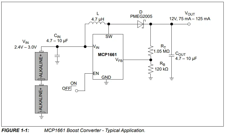
MCP1661 is a constant Pulse-Width Modulation (PWM) frequency boost (step-up) converter (see Figure 1-1), based on a Peak Current mode architecture which delivers high efficiency over a wide load range from two-cell and three-cell Alkaline, Energizer ® Ultimate Lithium, NiMH, NiCd and single-cell Li-Ion battery inputs. A high level of
integration lowers total system cost, eases implementation and reduces board area.
1.2.1 MCP1661 Key Features
- 36V, 800mΩ Integrated Switch
- Up to 92% Efficiency
- High Output Voltage Range: up to 32V
- 1.3A Peak Input Current Limit:
-IOUT > 200 mA @ 5V VIN, 12V VOUT
-IOUT > 125 mA @ 3.3V VIN, 12V VOUT
-IOUT > 100 mA @ 4.2V VIN, 24V VOUT - Input Voltage Range: 2.4V to 5.5V
- Undervoltage Lockout (UVLO):
-UVLO@VIN Rising: 2.3V, typical
-UVLO@VIN Falling: 1.85V, typical - No Load Input Current: 250 μA, typical
- Sleep Mode with 200 nA Typical Quiescent Current
- PWM Operation with Skip Mode: 500 kHz
- Cycle-by-Cycle Current Limiting
- Internal Compensation
- Inrush Current Limiting and Internal Soft-Start
- Output Overvoltage Protection (OVP) in the event of:
– Feedback pin shorted to GND
– Disconnected feedback divider - Overtemperature Protection
- Easy Configurable for SEPIC or Flyback Topologies
- Available Packages:
– 5-Lead SOT-23
– 2 mm x 3 mm 8-Lead TDFN
 1.3 FLYBACK CONVERTER TOPOLOGY OVERVIEW
The flyback converter is used in both AC/DC and DC/DC conversion having galvanic isolation between the input and one or more outputs. This type of converter is a derivation from a buck-boost converter with a transformer replacing the inductor, so that the voltage ratios are multiplied.
Being an isolated power converter, the control circuit needs to be isolated as well. There are two control types used for this converter: Voltage mode control and Current mode control; both require a signal related to the output voltage. This can be achieved either by using an optocoupler on the secondary circuitry to send a signal to the controller or by using a separate winding on the coil and rely on the cross regulation of the design.
The first approach involving an optocoupler is used to obtain very good voltage and current regulation, whereas the second was developed for cost-sensitive applications where the output does not need to be as precisely controlled, but simplifies the overall design considerably. In applications where reliability is critical, optocouplers should be
avoided.
In this application, a simpler technique (explained in the following chapters) was used, but its main drawback is that the voltage regulation is poor. Therefore, in order to overcome this and provide smooth regulation, an LDO was added at the isolated output of the flyback converter.
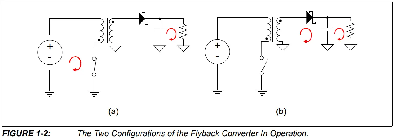
1.3.1 Flyback Converter Working Principle
The schematic of a flyback converter is depicted in Figure 2-1; it derives from the buck-boost topology, but utilizes a transformer instead of the inductor. A very important
aspect is that flyback transformers have an air gap which allows energy storing without risking the occurrence of core saturation. Therefore, the operating principle of both
converters is very close:
- When the switch is closed (Figure 1-2, a), the primary winding of the transformer is connected to the input voltage source. The primary current and magnetic flux in the transformer increases, storing energy in the transformer’s core. The voltage induced in the secondary winding is negative, so the diode is reverse-biased. In this phase, the output capacitor supplies energy to the output load (LDO’s input, in this application).
- When the switch is opened (Figure 1-2, b), the primary current and magnetic flux drops. The secondary voltage is positive, forward-biasing the diode, allowing current to flow from the transformer to the capacitor and to the load.
1.4 WHAT IS THE MCP1661 ISOLATED FLYBACK CONVERTER REFERENCE DESIGN?
The MCP1661 Isolated Flyback Converter Reference Design is used to evaluate and demonstrate Microchip Technology’s MCP1661 in the following topology:
- 5V output Isolated Flyback Converter application supplied from 5V typical input voltage.
It is used to evaluate the 5-Lead SOT-23 package.
By changing the LDO, a lower/higher output voltage than 5V will be obtained, but with different capabilities regarding maximum output current and efficiency.
1.5 WHAT DOES THE MCP1661 ISOLATED FLYBACK CONVERTER REFERENCE DESIGN KIT INCLUDE?
This MCP1661 Isolated Flyback Converter Reference Design kit includes:
- MCP1661 Isolated Flyback Converter Reference Design (ARD00598)
- Important Information Sheet
Chapter 2. Installation and Operation
2.1 INTRODUCTION
MCP1661 device is a non-synchronous, fixed-frequency step-up DC-DC converter which has been developed for applications that require higher output voltage capabilities. MCP1661 can regulate the output voltage up to 32V and can deliver 125 mA typical load at 3.3V input and 12V output. At light loads, MCP1661 skips pulses in order to keep the output voltage in regulation, but the voltage ripple is maintained low. The regulated output voltage should be greater than the input voltage.
2.1.1 Board Features
The MCP1661 Flyback Converter has the following features:
- Input Voltage: 4.25V – 5.25V, Typical
– USB standard input voltage range - Output Capability:
– Over 200 mA (at VOUT = 5V)
– Galvanic isolation
– Short-circuit protection - Efficiency: up to 75%
- PWM Operation at 500 kHz
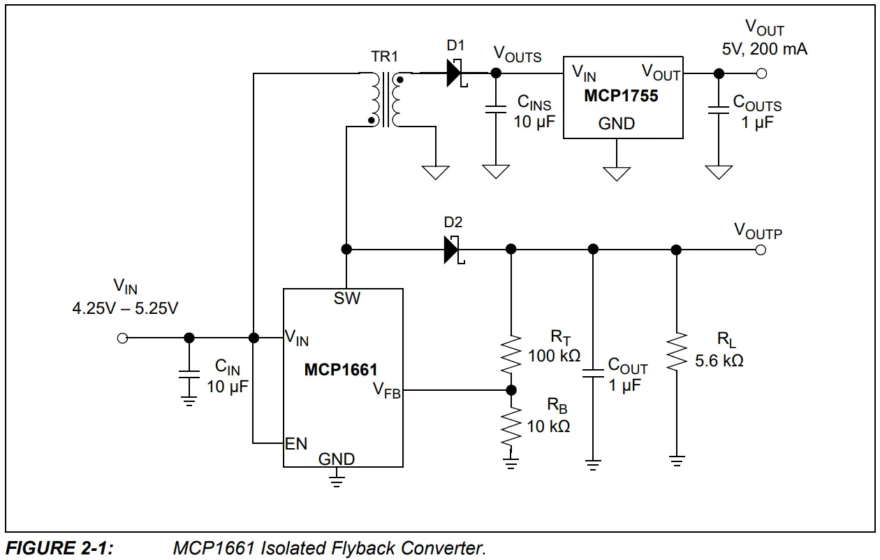
This application uses MCP1661 as an open-loop flyback converter, the primary winding of the transformer being used as inductor for the boost converter that clamps the primary output voltage (VOUTP) at around 13.5V. It is very important (for a normal operation of the entire circuitry and to avoid damaging some electronic components)
not to connect any additional load between VOUTP and GND. The output voltage of the flyback converter (VOUTS) drops with the increasing of output current, due to the fact that the feedback is taken from the primary side.
In order to achieve a very good output voltage regulation in the secondary side (VOUT), a 5V LDO is placed after the rectifying diode of the flyback converter, therefore the decrease of VOUTS when increasing the load is not critical.
The MCP1661 Isolated Flyback Converter Reference Design can be used for USB-powered applications, where a positive, regulated 5V output voltage is needed from an isolated input voltage that varies from 4.75V to 5.25V.
2.1.2 How Does the MCP1661 Isolated Flyback Converter Reference Design Work?
The converter is configured as non-synchronous; an external diode (D2) is connected between the inductor (primary winding of the transformer) and the high-voltage output (VOUTP). The chosen transformation ratio was 1:1, because the difference between the input voltage range (VIN) and the output voltage (VOUT) is small.
The output voltage of the flyback converter (VOUTS) decreases by increasing the load current, due to the lack of feedback from the secondary side of the transformer. The
amount of voltage drop (VOUTS) on the entire range of loads can be controlled by changing the load resistor RL. A higher dummy load for the primary side of the flyback
converter corresponds to a lower voltage drop in the secondary side (VOUTS) over the entire ourput current range, but the overall efficiency of the converter will decrease.
There is a compromise between the maximum output current capabilities, input voltage range and efficiency, by varying the values of the load resistor (RL) and feedback resistors (RT and RB). In this case, the values of the aforementioned electronic components were chosen in order to achieve good efficiency at 200 mA load current, up to 5.25V input voltage. The two sense resistors (RT and RB) set the output (VOUTP) at 13.5V, according to the following equation:
EQUATION 2-1: FEEDBACK RESISTORS RELATIONSHIP When designing such an application, special attention should be given to the values of the feedback resistors. When testing the board for a different output voltage, a potential issue related to the usage of higher value resistors might be caused by the environmental contamination, which can create a leakage current path on the Printed Circuit Board (PCB); this will affect the feedback voltage and the output voltage regulation. Engineers should utilize with precaution resistors that are larger than 1 MΩ.
In normal humidity conditions, the VFB pin input leakage current is very low and the resistors’ values will not affect the stability of the system.
All compensation and protection circuitry is integrated to minimize the number of external components. Ceramic input and output capacitors should be used.
Good efficiency is obtained at high load currents due to the decrease of the output voltage before the LDO (VOUTS).
2.2 GETTING STARTED
The MCP1661 Flyback Converter Reference Design is fully assembled and tested to evaluate and demonstrate the MCP1661 family of products.
2.2.1 Powering the MCP1661 Isolated Flyback Converter Reference Design
Input power connectors are placed on the left side of the board:
- VIN for positive power
- GND for negative power
The maximum input voltage should not exceed 5.5V; this can cause damage to the MCP1661.
The output connector is called VOUT; it is referenced to SGND and isolated from GND.
2.2.2 Board Testing
The variable power supply for testing requires output capability of at least 1A and a voltage range between 4V and 6V.
To test the board, follow next steps:
- Connect the power supply at VIN and GND terminals of the board.
- Set the power supply to 5V DC.
- Connect a voltmeter and a 100Ω/1W resistor between VOUT and SGND connectors, as shown in Figure 2-2. Check the voltmeter to make sure it indicates approximately 5V.
- Set the power supply to 4.75V and verify with the voltmeter if the output of the converter remains regulated (VOUT = 5V).
- Set the power supply to 5.25V and verify with the voltmeter if the output of the converter remains regulated (VOUT = 5V).
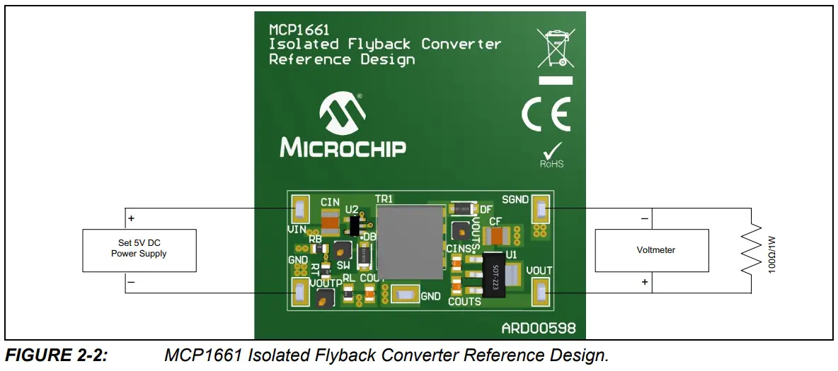
The board has several test points that help engineers analyze the switch node’s waveforms or MCP1661’s output:
- The test point of the MCP1661 device’s switch node (SW).
- VOUTP test point shows the MCP1661 boost’s output voltage (this output is regulated).
- VOUTS test point shows the MCP1661 flyback’s output voltage (this output is unregulated and is referenced to SGND).
The regulated output voltage of the boost converter (VOUTP) is about 13.5V and is referenced to GND.
2.2.3 Results
MCP1661 Isolated Flyback Converter uses an uncommon design, because the feedback voltage is taken from the primary side, so the output voltage in the secondary side (VOUTS) drops down as long as the load current increases (see Figure 2-3). However, the overall efficiency is still high, even if the LDO wastes some energy in order to keep the output voltage (VOUT) stable at 5V.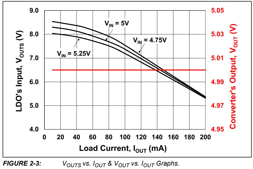
Refer to Figure 2-4 for the efficiency that can be obtained for different input voltages.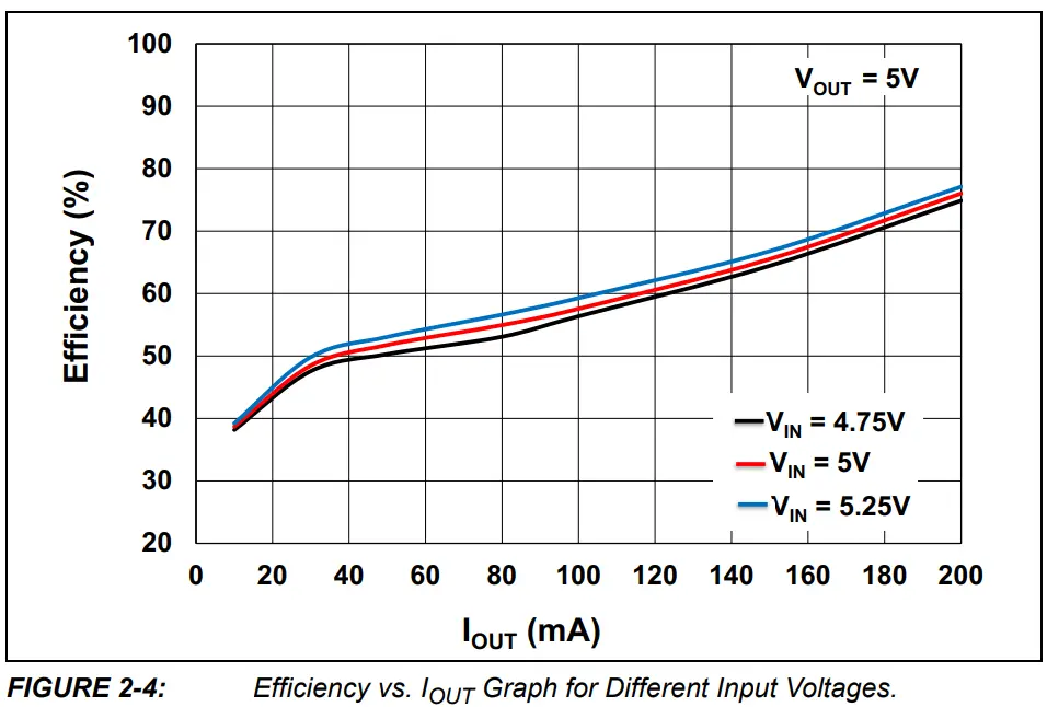 Figures 2-5 and 2-6 show the Discontinuous (at no load, 5V VIN) and Continuous Conduction Mode waveforms (50 mA load at 5V input voltage).
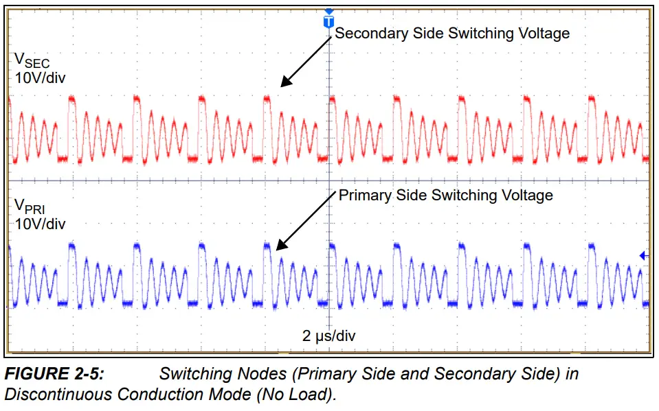
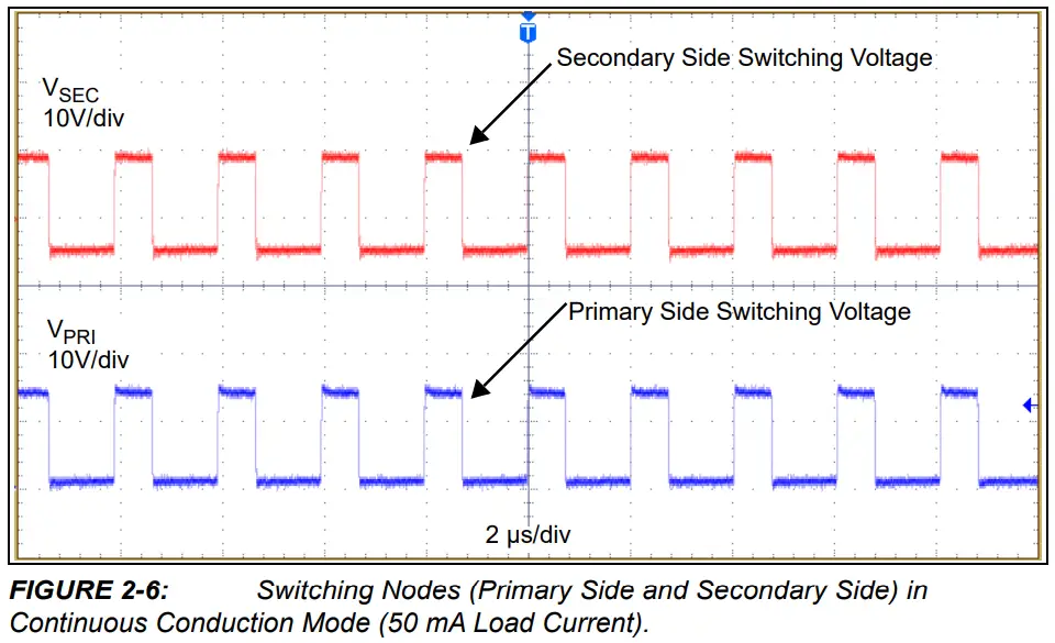 Figure 2-7 shows the start-up waveforms for MCP1661 Isolated Flyback Converter at 150 mA load current.
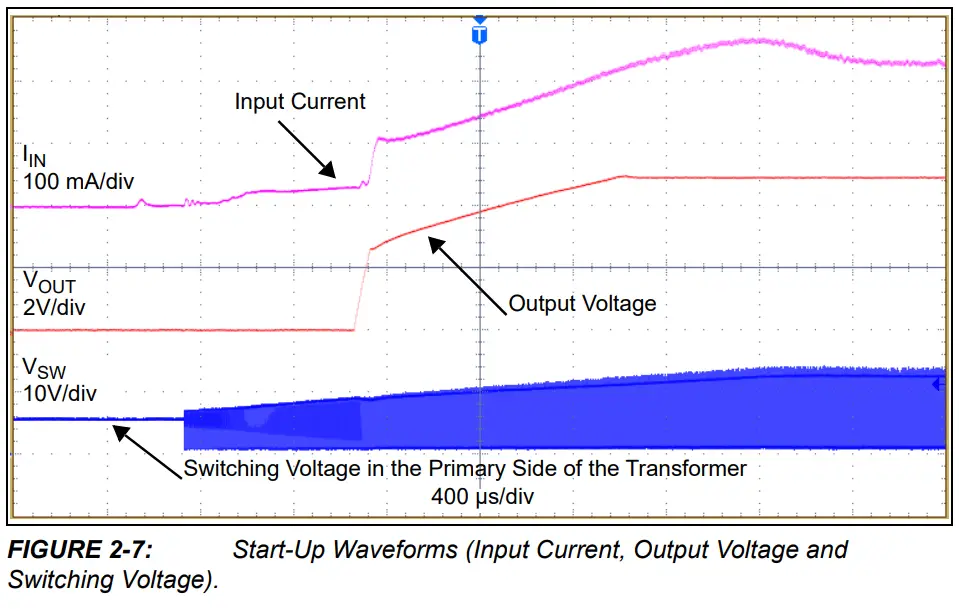
Appendix A. Schematic and Layouts
A.1 INTRODUCTION
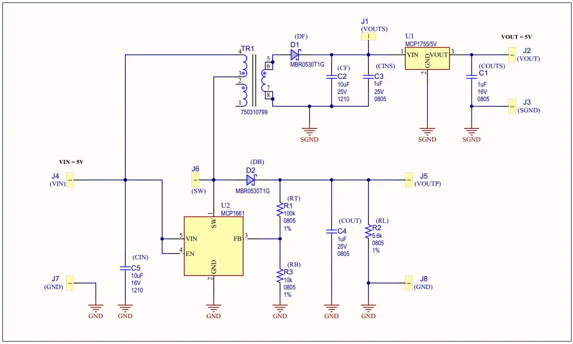
This appendix contains the following schematics and layouts for the MCP1661 Isolated Flyback Converter Reference Design:
- Board – Schematic
- Board – Top Silk
- Board – Top Copper and Silk
- Board – Top Copper
- Board – Bottom Copper
Schematic and Layouts
A.2BOARD – SCHEMATIC
A.3 BOARD – TOP SILK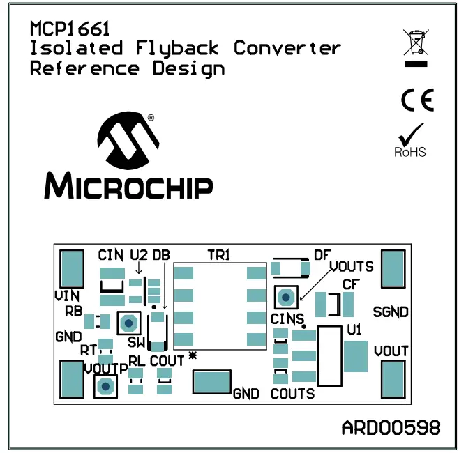 A.4 BOARD – TOP COPPER AND SILK
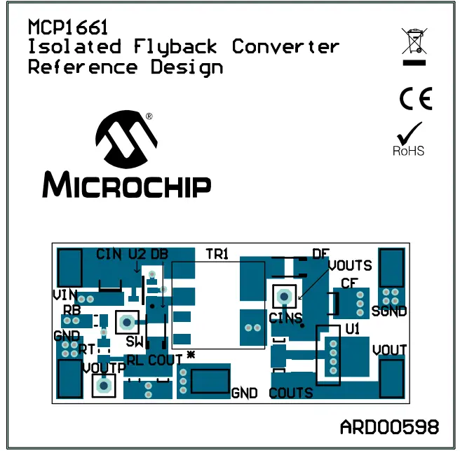 A.5 BOARD – TOP COPPER
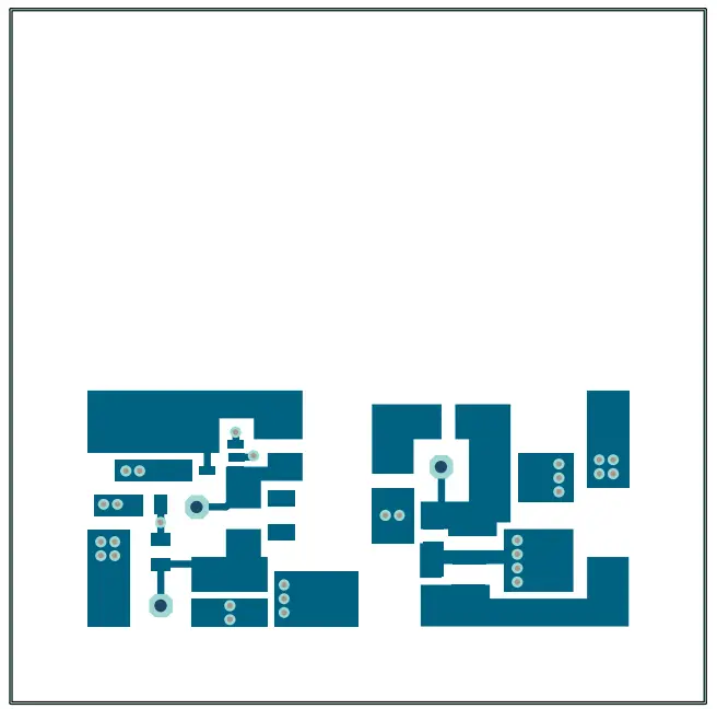 A.6 BOARD – BOTTOM COPPER
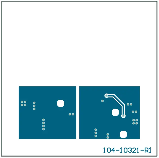
Appendix B. Bill of Materials
TABLE B-1: BILL OF MATERIALS (BOM)
| Qty. | Reference | Description | Manufacturer | Part Number |
| 1 | C1 | Capacitor, Ceramic, 1 pF, 16V, X7R, 0805 | TDK Corporation | C2012X7R1C105K125AA |
| 1 | C2 | Capacitor, Ceramic, 10 pF, 25V, X7R 1210 | TDK Corporation | C3225X7R1E106K250AC |
| 2 | C3, C4 | Capacitor, Ceramic, 1 pF, 25V, X7R, 0805 | TDK Corporation | C2012X7R1E105K125AB |
| 1 | C5 | Capacitor, Ceramic, 10 pF, 16V, X7R, 1210 | TDK Corporation | C3225X7R1C106K200AB |
| 2 | D1, D2 | Schottky, Rectifier, 30V, 0.5A. SOD123 | ON Semiconductor° | MBRO530T1G |
| 5 | J2, J3, J4, J7, J8 | PC Test Point TIN SMD | Harwin Plc. | 51751-46R |
| 1 | R1 | Resistor, 100 kf), 1/8W, 1%, 0805, SMD | Vishay/Dale | CRCW0805100KFKEA |
| 1 | R2 | Resistor, 5.6 kf), 1/8W, 1%, 0805, SMD | Vishay/Dale | CRCW08055K6OFKEA |
| 1 | R3 | Resistor, 10 kO, 1/8W, 1%, 0805, SMD | Vishay/Dale | CRCW080510KOFKEA |
| 1 | TR1 | Flyback Transformer, 25 pH, 15V, 1:1 | Wurth Elektronik | 750310799 |
Note 1: The components listed in this Bill of Materials are representative of the PCB assembly. The released BOM used in manufacturing uses all RoHS-compliant components.
TABLE B-2: BILL OF MATERIALS (BOM) – MICROCHIP PARTS
| Qty. | Reference | Description | Manufacturer | Part Number |
| 1 | PCB | MCP1661 Flyback Reference Design — Printed Circuit Board | Microchip Technology Inc. | 104-10321 |
| 1 | U1 | MCP1755S LDO 5V Output | Microchip Technology Inc. | MCP1755S-5002E/DB |
| 1 | U2 | MCP1661 High Voltage Boost Switcher, 500 kHz | Microchip Technology Inc. | MCP1661T-E/OT |
Note 1: The components listed in this Bill of Materials are representative of the PCB assembly. The released BOM used in manufacturing uses all RoHS-compliant components.
TABLE B-3: BILL OF MATERIALS (BOM) – DO NOT POPULATE PARTS
| Qty. | Reference | Description | Manufacturer | Part Number |
| 3 | J1, J5, J6 | Header, 2.54 mm, Vertical, THT | Samtec, Inc. | TSW-101-05-T-S |
Note 1: The components listed in this Bill of Materials are representative of the PCB assembly. The released BOM used in manufacturing uses all RoHS-compliant components.
Worldwide Sales and Service
| AMERICAS | ASIA/PACIFIC | ASIA/PACIFIC | EUROPE |
| Corporate Office 2355 West Chandler Blvd. Chandler, AZ 85224-6199 Tel: 480-792-7200 Fax: 480-792-7277 Technical Support: www.microchip.com/support Web Address: www.microchip.com Atlanta Duluth, GA Tel: 678-957-9614 Fax: 678-957-1455 Austin, TX Tel: 512-257-3370 Boston Westborough, MA Tel: 774-760-0087 Fax: 774-760-0088 Chicago Itasca, IL Tel: 630-285-0071 Fax: 630-285-0075 Dallas Addison, TX Tel: 972-818-7423 Fax: 972-818-2924 Detroit Novi, MI Tel: 248-848-4000 Houston, TX Tel: 281-894-5983 Indianapolis Noblesville, IN Tel: 317-773-8323 Fax: 317-773-5453 Tel: 317-536-2380 Los Angeles Mission Viejo, CA Tel: 949-462-9523 Fax: 949-462-9608 Tel: 951-273-7800 Raleigh, NC Tel: 919-844-7510 New York, NY Tel: 631-435-6000 San Jose, CA Tel: 408-735-9110 Tel: 408-436-4270 Canada – Toronto Tel: 905-695-1980 Fax: 905-695-2078 | Australia – Sydney Tel: 61-2-9868-6733 China – Beijing Tel: 86-10-8569-7000 China – Chengdu Tel: 86-28-8665-5511 China – Chongqing Tel: 86-23-8980-9588 China – Dongguan Tel: 86-769-8702-9880 China – Guangzhou Tel: 86-20-8755-8029 China – Hangzhou Tel: 86-571-8792-8115 China – Hong Kong SAR Tel: 852-2943-5100 China – Nanjing Tel: 86-25-8473-2460 China – Qingdao Tel: 86-532-8502-7355 China – Shanghai Tel: 86-21-3326-8000 China – Shenyang Tel: 86-24-2334-2829 China – Shenzhen Tel: 86-755-8864-2200 China – Suzhou Tel: 86-186-6233-1526 China – Wuhan Tel: 86-27-5980-5300 China – Xian Tel: 86-29-8833-7252 China – Xiamen Tel: 86-592-2388138 China – Zhuhai Tel: 86-756-3210040 | India – Bangalore Tel: 91-80-3090-4444 India – New Delhi Tel: 91-11-4160-8631 India – Pune Tel: 91-20-4121-0141 Japan – Osaka Tel: 81-6-6152-7160 Japan – Tokyo Tel: 81-3-6880- 3770 Korea – Daegu Tel: 82-53-744-4301 Korea – Seoul Tel: 82-2-554-7200 Malaysia – Kuala Lumpur Tel: 60-3-7651-7906 Malaysia – Penang Tel: 60-4-227-8870 Philippines – Manila Tel: 63-2-634-9065 Singapore Tel: 65-6334-8870 Taiwan – Hsin Chu Tel: 886-3-577-8366 Taiwan – Kaohsiung Tel: 886-7-213-7830 Taiwan – Taipei Tel: 886-2-2508-8600 Thailand – Bangkok Tel: 66-2-694-1351 Vietnam – Ho Chi Minh Tel: 84-28-5448-2100 | Austria – Wels Tel: 43-7242-2244-39 Fax: 43-7242-2244-393 Denmark – Copenhagen Tel: 45-4485-5910 Fax: 45-4485-2829 Finland – Espoo Tel: 358-9-4520-820 France – Paris Tel: 33-1-69-53-63-20 Fax: 33-1-69-30-90-79 Germany – Garching Tel: 49-8931-9700 Germany – Haan Tel: 49-2129-3766400 Germany – Heilbronn Tel: 49-7131-72400 Germany – Karlsruhe Tel: 49-721-625370 Germany – Munich Tel: 49-89-627-144-0 Fax: 49-89-627-144-44 Germany – Rosenheim Tel: 49-8031-354-560 Israel – Ra’anana Tel: 972-9-744-7705 Italy – Milan Tel: 39-0331-742611 Fax: 39-0331-466781 Italy – Padova Tel: 39-049-7625286 Netherlands – Drunen Tel: 31-416-690399 Fax: 31-416-690340 Norway – Trondheim Tel: 47-72884388 Poland – Warsaw Tel: 48-22-3325737 Romania – Bucharest Tel: 40-21-407-87-50 Spain – Madrid Tel: 34-91-708-08-90 Fax: 34-91-708-08-91 Sweden – Gothenberg Tel: 46-31-704-60-40 Sweden – Stockholm Tel: 46-8-5090-4654 UK – Wokingham Tel: 44-118-921-5800 Fax: 44-118-921-5820 |
![]() DS50002313B
DS50002313B
2014-2022 Microchip Technology Inc. and its subsidiaries


