![]()
User Guide | EVAL-AD8411A
UG-2112
Evaluating the AD8411A, −2 V to 70 V Wide Input Voltage Range, 2.7 MHz High Bandwidth,
Current-Sense Amplifier with PWM Rejection and Gain 50 V/V
FEATURES
► Enables quick breadboarding and prototyping
► Easily configurable for unidirectional or bidirectional operation
► Includes provision for current-sense shunt resistor
► Easy connection to test equipment
► Includes provisions for an input filter and an output filter
► Decoupled supply line
EVALUATION KIT CONTENTS
► AD8411ARM-EVALZ evaluation board
DOCUMENTS NEEDED
► AD8411A data sheet
GENERAL DESCRIPTION
The AD8411ARM-EVALZ is designed to aid in the evaluation of the AD8411A current-sense amplifier. These boards are designed for easy configuration of different modes of operation and allow flexibility with loads. A shunt resistor (R1), with a maximum standard size of 2818, can be soldered to the board.
The AD8411ARM-EVALZ accommodates the AD8411A in a mini small outline package (MSOP).
Full specifications on the AD8411A are available in the AD8411A data sheet available from Analog Devices, Inc., and must be consulted with this user guide when using the AD8411ARM-EVALZ evaluation board.
REVISION HISTORY
4/2023—Revision 0: Initial Version
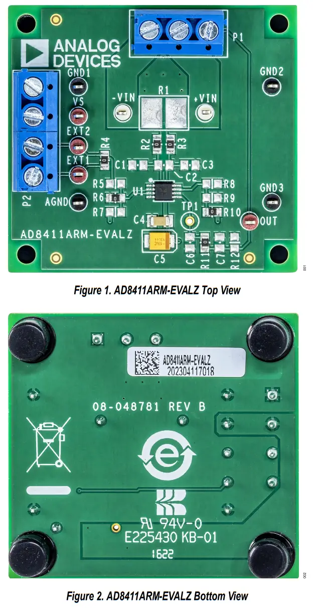
AD8411ARM-EVALZ EVALUATION BOARD PHOTOGRAPHS
QUICK START
By default, VREF1 is connected to VS, and VREF2 is connected to the GND pin. This split supply configuration sets the output to midsupply and allows bidirectional current sensing. Connect 5 V to the VS test point on the evaluation board, connect the ground of the supply to the AGND test point on the evaluation board, and place a 0.04 V differential voltage between the +VIN test point and the −VIN test point on the evaluation board. This small 0.04 V differential input voltage represents the voltage drop across the shunt resistor that is used in the application.
VOUT = 2.5V+ VDIFF × GAIN (1)
After the evaluation board is powered, the output reads as:
4.5V = 2.5V+ 0.04V × 50V/V (2)
Then swap the input differential voltage leads (move the lead on the
+VIN test point to the −VIN test point and move the lead that was
on the −VIN test point to the +VIN test point). The output then reads as:
0.5V = 2.5V− 0.04V × 50V/V (3)
POWER SUPPLIES
The AD8411A has a power-supply operating range from 2.9 V to 5.5 V. Power is applied to the VS test point. Decoupling capacitors of 10 µF and 0.1 µF are preinstalled on the evaluation board.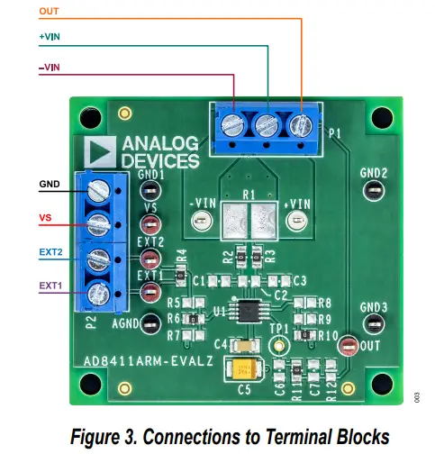
COMPONENTS
The AD8411A can be used for a variety of current monitoring applications. The AD8411ARM-EVALZ has a provision for a currentsense shunt resistor with a maximum standard size of 2818. There are also provisions with 0805 footprints for a capacitive-load, a resistive load, an input electromagnetic interference (EMI) filter, an output
filter, and provisions to set the reference voltage. Terminal blocks (P1 and P2) are provided to allow easy wiring and evaluation.Table 1. VREF1 Pin Connections
SETTING THE REFERENCE VOLTAGE
Three resistor spaces (R5, R6, and R7) are on the left side of the AD8411A on the AD8411ARM-EVALZ. These three resistors are used to set VREF2. Fill only one of these resistor spaces at a time with a 0 Ω, 0805 resistor. See Table 2 for the resistors that must be
filled with 0 Ω to resistor to set VREF2.
Three resistor spaces (R8, R9, and R10) are on the right side of the AD8411A on the AD8411ARM-EVALZ. These three resistors are used to set VREF1. Fill only one of hese resistor spaces at a time with a 0 Ω, 0805 resistor. See Table 1 for the resistors that must be filled with 0 Ω to resistor to set VREF1.
Table 1. VREF1 Pin Connections
| Pin R8 R9 R10 | |||
| vs | |||
| GND | X | ✓ | X |
| EXT1 | ✓ | X | X |
Table 2. VREF2 Pin Connections
| Pin R5 R6 R7 | |||
| vs | |||
| GND | X | ✓ | X |
| EXT2 | ✓ | X | X |
Unidirectional Operation
For unidirectional operation, the output can be set at the negative rail (near ground) or at the positive rail (near the supply voltage) when the differential voltage is 0 V. To set the AD8411ARM-EVALZ for a ground-referenced output, solder the 0 Ω resistor on the left side of the AD8411A in the R6 space and the 0 Ω resistor on the right side of the AD8411A in the R9 space.
To set the AD8411ARM-EVALZ for a supply voltage referenced output, solder the 0 Ω resistor on the left side of the AD8411A in the R7 space and the 0 Ω resistor on the right side of the AD8411A in the R10 space.
Bidirectional Operation
For a bidirectional operation, the output is typically set at half-scale for an equal range in both directions. To configure the output to be at midsupply in the presence of 0 A of current through the shunt resistor on the AD8411ARM-EVALZ, solder the 0 Ω resistor on the left side of the AD8411A in the R6 space and the 0 Ω resistor on the
right side of the AD8411A in the R10 space.
By default, the output of the AD8411ARM-EVALZ is biased at midsupply.
Table 3 shows which resistor must be filled with 0 Ω resistor to set the AD8411ARM-EVALZ for different operations. In unidirectional operation, it can be ground- eferenced output and supply
QUICK START
voltage-referenced output, whereas, in the bidirectional operation, the output can be set to midsupply.
Table 3. Operation Connection
| Mode R6 R7 R9 R10 | ||||
| UNIDIRECTIONAL Ground Referenced Supply Voltage Referenced | ii. x | X | rna. x | 1 x ai. |
| BIDIRECTIONAL Midsupply | ✓ | X | X | ✓ |
External Referenced Output
An external supply can also be used to set the reference voltage. To bias the output to a single external supply, solder a 0 Ω, 0805 resistor in the R4 space. Then, solder the 0 Ω resistor on the left side of the AD8411A in the R5 space and solder the 0 Ω resistor on the right side of the AD8411A in the R8 space. The external supply voltage can then be applied to any one of the EXTx test points onthe evaluation board, and this configuration biases the output to the external supply.
The external supply can also be divided by 2 and used as a reference level. For this reference level, solder the 0 Ω resistor on the left side of the AD8411A in the R6 space, desolder the resistor in the R4 space, and solder the 0 Ω resistor on the right side of the AD8411A in the R8 space. Apply the external supply to the EXT1 test point or EXT1 terminal block input, and the output of the AD8411A is referenced to half of the external supply.
Two separate external supplies can also be used to set the reference for the output. Desolder the 0 Ω resistor from the R4 space. Solder the 0 Ω resistor on the left side of the
AD8411A in the R5 space and solder the 0 Ω resistor on the right side of the AD8411A in the R8 space. Apply the first external supply, VEXT1, to the EXT1 test point or EXT1 terminal block input. Apply the second external supply, VEXT2, to the EXT2 test point or EXT2 terminal block input. This configuration references the output to:
![]()
INPUT FILTER
The AD8411ARM-EVALZ includes provisions for the components necessary for an input filter. By default, R2 and R3 are 0 Ω, 0805 resistors and C1, C2, and C3 are left unpopulated. It is requiredto filter at the input of the device to reduce EMI. The EMI specifications vary depending on the application. Filtering at the input must be referred if the output cannot be filtered because filtering at the output changes the low output impedance seen by the components attached to the output of the AD8411A. The +IN and –IN inputsof the AD8411A has balanced input bias currents. This means that the input series resistors, R2 and R3, must be the same measured value not to have a large offset voltage added to the output of thedevice as a result of R2 and R3. It is recommended to keep R2 and R3 below 100 Ω.
The EMI filter has two different bandwidths, common-mode (BWCM) and differential (BWDIFF). The differential bandwidth defines the frequency response of the filter with a differential input signal applied between the two inputs of the amplifier, which are +IN and −IN. C1 and C3 must be the same value for the following equations.
The −3 dB differential bandwidth for the filter is:
![]()
The common-mode bandwidth defines what a common-mode RF signal experiences between ground and the +IN and –IN inputs of the amplifier tied together.
The −3 dB common-mode bandwidth for the filter is:
![]()
Keep the resistor values to a 1% tolerance and the filter capacitors to a 5% tolerance to assist with reducing AC common-mode rejection (CMR) errors. Choose C2 to be at least 10× larger than C1 or C3 to reduce AC CMR errors, which are caused by component mismatching.
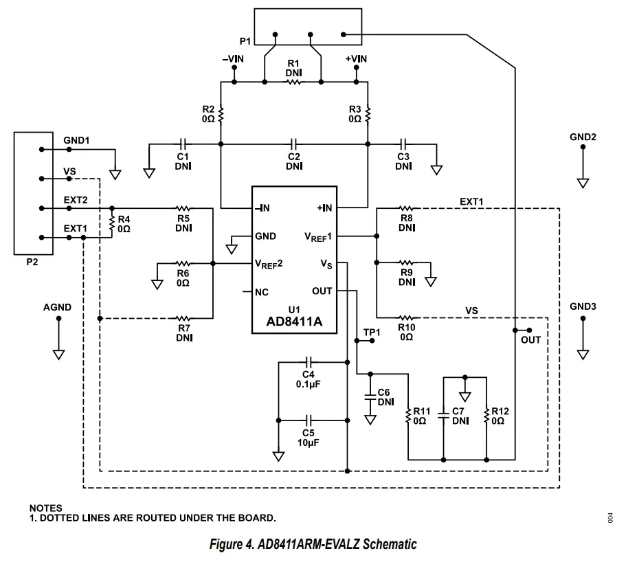
Figure 1 shows the top view and Figure 2 shows the bottom view of the AD8411ARM-EVALZ. Figure 4 shows the default schematic of the AD8411ARM-EVALZ. The otted lines in the AD8411ARMEVALZ schematic are routed under the printed circuit board (PCB).
EVALUATION BOARD SCHEMATIC
ORDERING INFORMATION
BILL OF MATERIALS
| Item | Quantity | Reference Designator | Part Description | Manufacturer, Part Number |
| 1 2 | 1 2 4 1 1 4 1 1 6 4 5 1 5 1 | U1 +VIN, −VIN AGND, GND1, GND2, GND3 C4 C5 EXT1, EXT2, OUT, VS P1 P2 R2, R3, R4, R6, R10, R11 Standard Grip C1, C2, C3, C6, C7 R1 R5, R7, R8, R9, R12 TP1 | IC, High voltage, high bandwidth, current-sense amplifier,automotive Connectors-PCB, test point white Connectors-PCB, test point black Capacitor, CER, 0.1 μF, 50 V, 10%, X7R, 1206 Capacitor, TANT, 10 μF, 16 V, 10%, 3528-20 Connectors-PCB, test point red Connector-PCB, terminal block VERT, 5 mm pitch Connector-PCB, terminal block, 5 mm pitch, 3.5 mm solder tail Resistors, SMD, 0 Ω, 1/10 W, 0805 Miscellaneous, Bumper cylindrical, size 0.312″ Dia (7.92 mm), thickness 0.215″ (5.46 mm), black with adhesive Not installed, Capacitors, C0805 Not installed, Resistor, 2818 Not installed, Resistors, R0805 Connector-PCB, test point black | Analog Devices Inc., AD8411AWBRMZ Keystone Electronics, 5002 Keystone Electronics, 5001 Yageo, CC1206KRX7R9BB104 AVX Corporation, TAJB106K016RNJ Keystone Electronics, 5000 On Shore Technology, OSTTC030162 On shore Technology, OSTTC040162 Multicomp (SPC), MC 0.1 W 0805 0R 3M, SJ61A6 Not Applicable Vishay, WSHM2818R0500FEA Not Applicable Keystone Electronics, 5001 |
![]() ESD Caution
ESD Caution
ESD (electrostatic discharge) sensitive device. Charged devices and circuit boards can discharge without detection. Although this product features patented or proprietary protection circuitry, damage may occur on devices subjected to high energy ESD. Therefore, proper ESD precautions should be taken to avoid performance degradation or loss of functionality.
Legal Terms and Conditions
By using the evaluation board discussed herein (together with any tools, components documentation or support materials, the “Evaluation Board”), you are agreeing to be bound by the terms and conditions set forth below (“Agreement”) unless you have purchased the Evaluation Board, in which case the Analog Devices Standard Terms and Conditions of Sale shall govern. Do not use the Evaluation Board until you have read and agreed to the Agreement. Your use of the Evaluation Board shall signify your acceptance of the Agreement. This Agreement is made by and between you (“Customer”) and Analog Devices, Inc. (“ADI”), with its principal place of business at Subject to the terms and conditions of the Agreement, ADI hereby grants to Customer a free, limited, personal, temporary, non-exclusive, non-sublicensable, non-transferable license to use the Evaluation Board FOR EVALUATION PURPOSES ONLY. Customer understands and agrees that the Evaluation Board is provided for the sole and exclusive purpose referenced above, and agrees not to use the Evaluation Board for any other purpose. Furthermore, the license granted is expressly made subject to the following additional limitations: Customer shall not (i) rent, lease, display, sell, transfer, assign, sublicense, or distribute the Evaluation Board; and (ii) permit any Third Party to acce s
the Evaluation Board. As used herein, the term “Third Party” includes any entity other than ADI, Customer, their employees, affiliates and in-house consultants. The Evaluation Board is NOT sold to Customer; all rights not expressly granted herein, including ownership of the Evaluation Board, are reserved by ADI. NFIDENTIALITY. This Agreement and the Evaluation Board shall all be considered the confidential and proprietary information of ADI. Customer may not disclose or transfer any portion of the Evaluation Board to any other party for any reason. Upon discontinuation of use of the Evaluation Board or termination of this Agreement, Customer agrees to promptly return the Evaluation Board to ADI. ADDITIONAL RESTRICTIONS. Customer may not disassemble, decompile or reverse engineer chips on the Evaluation Board. Customer shall inform ADI of any occurred damages or any modifications or alterations it makes to the Evaluation Board, including but not limited to soldering or any other activity that affects the material content of the Evaluation Board. Modifications to the Evaluation Board must comply with applicable law, including but not limited to the RoHS Directive. TERMINATION. ADI may terminate this Agreement at any time upon giving written notice to Customer. Customer agrees to return to ADI the Evaluation Board
at that time. LIM TATION OF LIABILITY. THE EVALUATION BOARD PROVIDED HEREUNDER IS PROVIDED “AS IS” AND ADI MAKES NO WARRANTIEE IMPLIED WARRANTY OF MERCHANTABILITY, TITLE, FITNESS FOR A PARTICULAR PURPOSE OR NONINFRINGEMENT OF
INTELLECTUAL PROPERTY RIGHTS. IN NO EVENT WILL ADI AND ITS LICENSORS BE LIABLE FOR ANY INCIDENTAL, SPECIAL, INDIRECT, OR CONSEQUENTIAL DAMAGES RESULTING FROM CUSTOMER’S POSSESSION OR USE OF THE EVALUATION BOARD, INCLUDING BUT NOT IMITED TO LOST PROFITS, DELAY COSTS, LABOR COSTS OR LOSS OF GOODWILL. ADI’S TOTAL LIABILITY FROM ANY AND ALL CAUSES SHALL BE LIMITED TO THE AMOUNT OF ONE HUNDRED US DOLLARS ($100.00). EXPORT. Customer agrees that it will not directly or indirectly export the Evaluation Board to another country, and that it will comply with all applicable United States federal laws and regulations relating to exports. GOVERNING LAW. This Agreement
shall be governed by and construed in accordance with the substantive laws of the Commonwealth of Massachusetts (excluding conflict of law rules). Any legal action regarding this Agreement will be heard in the state or federal courts having jurisdiction in Suffolk County, Massachusetts, and Customer hereby submits to the personal jurisdiction and venue of such courts. The United Nations Convention on Contracts for the International Sale of Goods shall not apply to this Agreement and is expressly disclaimed.
![]()
©2023 Analog Devices, Inc. All rights reserved. Trademarks and registered trademarks are the property of their respective owners. One Analog Way, Wilmington, MA 01887-2356, U.S.A.


