UM2944 Steval-1PS03A Evaluation Board Based on ST1PS03AQTR User Manual

Introduction
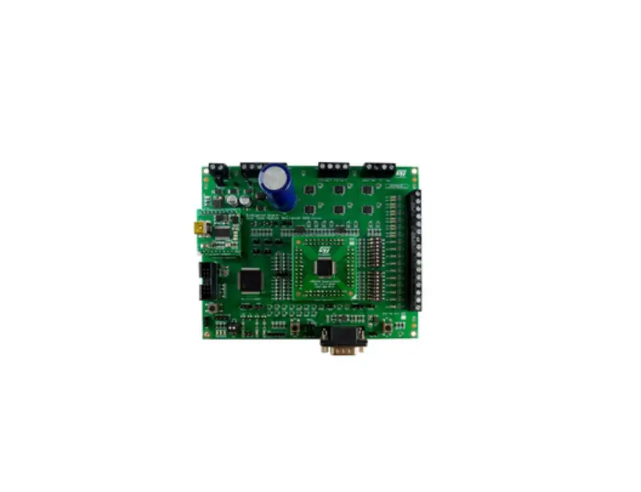
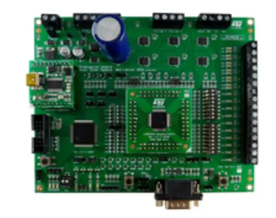
The STEVAL-1PS03A is an evaluation board for a smart converter design able to deliver up to 400 mA output current from a 1.8 to 5.5 V input, with a 1.6 to 3.3 V dynamically adjustable output voltage.
The board features the ST1PS03AQTR nano-quiescent miniaturized synchronous step-down converter, which implements enhanced peak current control (PCC) and advanced design circuitry to minimize quiescent current. The device embeds a controlled load switch to supply a subsystem with VIN_AUX voltage rail.
The STEVAL-1PS03A demonstrates how highly efficient conversion can be achieved thanks to the ST1PS03AQTR (in a thin TQFN12 package of 2.0×1.7 mm), a 2.2 μH inductor, and two small capacitors.
The ST1PS03AQTR key application benefits include high efficiency, and small PCB size and thickness. It is extremely suitable for power conversion solutions in wearable applications and fitness accessories, personal tracking monitoring, smart watches, sport bands, energy harvesting, wireless sensors, industrial sensors, portable low-power devices, single cell Li-ion battery
applications, as well as Bluetooth® low energy and Zigbee applications.
1 Getting started
1.1 Features
- 1.8 to 5.5 V input operating range
- Up to 400 mA output current capability
- Tiny external components: L = 2.2 μH typ
- Dynamically selectable output voltages from 1.6 to 3.3 V
- Output voltage Power Good
- Independent load switch (AUX control input)
- WEEE and RoHS compliant (hardware only)
1.2 Electrical performance specification
Table 1. Electrical performance specification (Ta = 25°C) Symbol Parameter Min.
| Symbol | Parameter | Min. | Typ. | Max. | Unit |
| VIN | Input supply voltage | 1.8 | 3.6 | 5.5 | V |
| VIN_AUX | Auxiliary input supply voltage | 0 | VIN | V | |
| VOUT range | Programmable by D0, D1 and D2 (see Table 2) | 1.6 | 3.3 | V | |
| IOUT | Output current | 400 | mA | ||
| IOUT_AUX | Auxiliary output current | 100 | mA |
Table 2. Output voltage settings
| Device | D2 | D1 | D0 | VOUT |
|
| 0 | 0 | 0 | 1.8 V |
| 0 | 0 | 1 | 3.3 V | |
| 0 | 1 | 0 | 2.8 V | |
| 0 | 1 | 1 | 2.7 V | |
| 1 | 0 | 0 | 3.0 V | |
| 1 | 0 | 1 | 2.1 V | |
| 1 | 1 | 0 | 1.6 V | |
| 1 | 1 | 1 | 2.5 V |
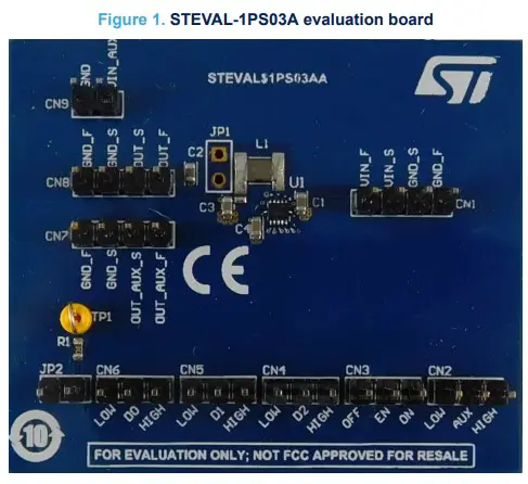
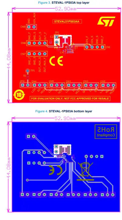
1.3 Input/output connector descriptions
This section provides the descriptions of the input/output connectors of the STEVAL-1PS03A.
- CN1: main input power supply
- VIN_F: positive input power force
- VIN_S: positive input power sense
- GND_F: ground input force
- GND_S: ground input sense
- CN9: auxiliary input power supply
- VIN_AUX: auxiliary input voltage
- GND: ground
- CN8: output voltage connector
- OUT_F: output voltage force
- OUT_S: output voltage sense
- GND_F: ground output force
- GND_S: ground output sense
- CN9: auxiliary output voltage connector
- OUT_F: auxiliary output voltage force
- OUT_S: auxiliary output voltage sense
- GND_F: ground output force
- GND_S: ground output sense
- CN2: load switch selection pin
- Place the jumper across AUX and HIGH to enable the load
- Place the jumper across AUX and LOW to disable the load
- CN3: ENABLE pin
- Place the jumper across EN and HIGH to enable the buck
- Place the jumper across EN and LOW to disable the buck
- CN4, CN5, CN6: output voltage selection pins (see Table 2, output voltage settings for VOUT selection).
Important: Do not leave these pins floating. They can be dynamically changed during operation.
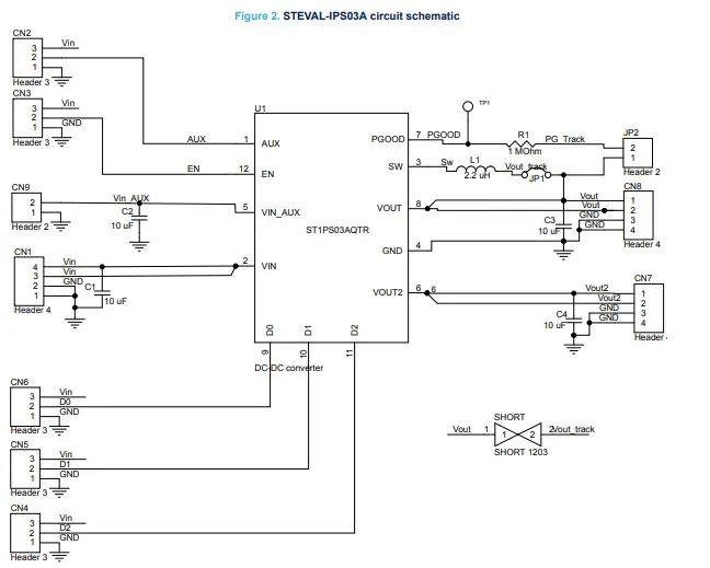
Schematic diagrams
Figure 2. STEVAL-IPS03A circuit schematic
Bill of materials
Table 3. STEVAL-1PS03A1 bill of materials
| Item | Q.ty | Ref. | Value | Description | Manufacturer | Part Number |
| 1 | 1 | R1 | 1 MΩ, SMD 0603, 0.25 W, ±1 % | Thick film resistor | Vishay | CRCW06031M00FKEAHP |
| 2 | 4 | C1, C2, C3, C4 | 10 µF, SMD 0603, 16 V, ±20 %, X5R | Ceramic capacitors | TDK | C1608X5R1C106M080AB |
| 3 | 1 | L1 | 2.2 µH, SMD 1008, 2.6 A, ±20 % | Inductor for power circuits | TDK | VLS252010HBX-2R2M-1 |
| 4 | 1 | U1 | ST1PS03AQTR, TQFN12 | Nano-quiescent synchronous step- down converter | ST | |
| 5 | 1 | TP1 | Test pin, through hole | Test point | Multicomp | TEST-1(Y) |
| 6 | 2 | JP2, CN9 | 2×1, through hole, 3 A, pitch 2.54 mm | Male SIL vertical connectors | Harwin | M20-9993645 |
| 7 | 5 | CN2, CN3, CN4, CN5, CN6 | 3×1, through hole, 3 A, pitch 2.54 mm | Male SIL vertical connectors | Harwin | M20-9993645 |
| 8 | 3 | CN1, CN7, CN8 | 4×1, through hole, 3 A, pitch 2.54 mm | Male SIL vertical connectors | Harwin | M20-9993645 |
| 9 | 1 | JP1 | Short-circuit, through hole | Soft tinned copper wire | RS Pro | 390-549 |
4. Board layout
5 Board versions
Table 4. STEVAL-IPS03A versions
| Finished good | Schematic diagrams | Bill of materials |
| STEVAL$1PS03AA (1) | STEVAL$1PS03AA schematic diagrams | STEVAL$1PS03AA bill of materials |
- This code identifies the STEVAL-1PS03A evaluation board first version.
6 Regulatory compliance
Formal Notice Required by the U.S. Federal Communications Commission
FCC NOTICE:
This kit is designed to allow:
- Product developers to evaluate electronic components, circuitry, or software associated with the kit to determine whether to incorporate such items in a finished product and
- Software developers to write software applications for use with the end
This kit is not a finished product and when assembled may not be resold or otherwise marketed unless all required FCC equipment authorizations are first obtained. Operation is subject to the condition that this product not cause harmful interference to licensed radio stations and that this product accept harmful interference. Unless the assembled kit is designed to operate under part 15, part 18 or part 95 of this chapter, the operator of the kit must operate under the authority of an FCC license holder or must secure an experimental authorization under part 5 of this chapter 3.1.2.
The evaluation kit has been designed to comply with part 15 of the FCC Technical Rules. Operation is subject to the following two conditions: (1) This device may not cause harmful interference, and (2) this device must accept any interference received, including interference that may cause undesired operation.
This equipment has been tested and found to comply with the limits for a Class B digital device, pursuant to part 15 of the FCC Rules. These limits are designed to provide reasonable protection against harmful interference
in a residential installation. This equipment generates, uses and can radiate radio frequency energy and, if not installed and used in accordance with the instructions, may cause harmful interference to radio communications. However, there is no guarantee that interference will not occur in a particular installation.
Standard applied: FCC CFR 47 Part 15 Subpart B. Test method applied: ANSI C63.4 (2014).
Formal Product Notice Required by Industry Canada Innovation, Science and Economic Development Canada compliance:
For evaluation purposes only. This kit generates, uses, and can radiate radio frequency energy and has not been tested for compliance with the limits of computing devices pursuant to Industry Canada (IC) rules. À des fins d’évaluation uniquement. Ce kit génère, utilise et peut émettre de l’énergie radiofréquence et n’a pas été testé pour sa conformité aux limites des appareils informatiques conformément aux règles d’Industrie Canada (IC). This device has been tested with Innovation, Science and Economic Development RSS standards. Operation is subject to the following two conditions: (1) this device may not cause harmful interference, and (2) this device must accept any interference received, includin g interference that may cause undesired operation.
Standard applied: ICES-003 Issue 7 (2020), Class B. Test method applied: ANSI C63.4 (2014).Cet appareil a été testé pour les normes RSS d’Innovation, Science et Développement économique. L’utilisation est soumise aux deux conditions suivantes: (1) cet appareil ne doit pas causer d’interférences nuisibles, et (2) cet appareil doit accepter de recevoir tous les types d’interférence, y comprises les interférences susceptibles d’entraîner un fonctionnement indésirable.
Norme appliquée: NMB-003, 7e édition (2020), Classe B. Méthode d’essai appliquée: ANSI C63.4 (2014).
Formal product notice required by EU
This device is in conformity with the essential requirements of the Directive 2014/30/EU (EMC) and of the Directive 2015/863/EU (RoHS).
Standards applied (Class B): EN 61000-6-1:2019, EN 61000-6-3:2007 + A1:2011 + AC:2012, EN 55032:2015 + A1:2020, EN 55035:2017 + A11:2020, EN 61000-3-2:2019, EN 61000-3-3:2013 + A1:2019
Revision history
Table 5. Document revision history
| Date | Revision | Changes |
| 19-Oct-2021 | 1 | Initial release. |
IMPORTANT NOTICE – PLEASE READ CAREFULLY
STMicroelectronics NV and its subsidiaries (“ST”) reserve the right to make changes, corrections, enhancements, modifications, and improvements to ST products and/or to this document at any time
without notice. Purchasers should obtain the latest relevant information on ST products before placing orders. ST products are sold pursuant to ST’s terms and conditions of sale in place at the time of order
acknowledgement.
Purchasers are solely responsible for the choice, selection, and use of ST products and ST assumes no liability for application assistance or the design of Purchasers’ products.
No license, express or implied, to any intellectual property right is granted by ST herein.
Resale of ST products with provisions different from the information set forth herein shall void any warranty granted by ST for such product.
ST and the ST logo are trademarks of ST. For additional information about ST trademarks, please refer to www.st.com/trademarks. All other product or service names are the property of their respective owners.
Information in this document supersedes and replaces information previously supplied in any prior versions of this document.
© 2021 STMicroelectronics – All rights reserved


