VISHAY SiHG460B D Series Power MOSFET User Manual

D Series Power MOSFET
| PRODUCT SUMMARY | ||
| VDS (V) at TJ max. | 550 | |
| RDS(on) max. at 25 °C (W) | VGS = 10 V | 0.25 |
| Qg max. (nC) | 170 | |
| Qgs (nC) | 14 | |
| Qgd (nC) | 28 | |
| Configuration | Single | |
FEATURES
- Optimal Design
– Low Area Specific On-Resistance
– Low Input Capacitance (Ciss)
– Reduced Capacitive Switching Losses
– High Body Diode Ruggedness
– Avalanche Energy Rated (UIS) - Optimal Efficiency and Operation
– Low Cost
– Simple Gate Drive Circuitry
– Low Figure-of-Merit (FOM): Ron x Qg
– Fast Switching - Material categorization: For definitions of compliance
please see www.vishay.com/doc?99912
Note - Lead (Pb)-containing terminations are not RoHS-compliant.
Exemptions may apply
| ORDERING INFORMATION | |
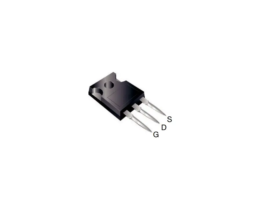
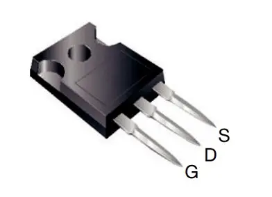
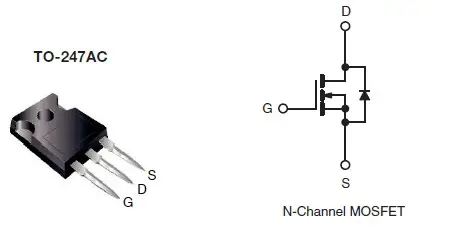
| Package | TO-247AC |
| Lead (Pb)-free | IRFP460BPbF |
| Lead (Pb)-free and Halogen-free | SiHG460B-GE3 |
| ABSOLUTE MAXIMUM RATINGS (TC = 25 °C, unless otherwise noted) | |||||
| PARAMETER | SYMBOL | LIMIT | UNIT | ||
| Drain-Source Voltage | VDS | 500 | V | ||
| Gate-Source Voltage | VGS | ± 20 | |||
| Gate-Source Voltage AC (f > 1 Hz) | 30 | ||||
| Continuous Drain Current (TJ = 150 °C) | VGS at 10 V | TC = 25 °C | ID | 20 | A |
| TC = 100 °C | 13 | ||||
| Pulsed Drain Currenta | IDM | 62 | |||
| Linear Derating Factor | 2.2 | W/°C | |||
| Single Pulse Avalanche Energyb | EAS | 281 | mJ | ||
| Maximum Power Dissipation | PD | 278 | W | ||
| Operating Junction and Storage Temperature Range | TJ, Tstg | – 55 to + 150 | °C | ||
| Drain-Source Voltage Slope | TJ = 125 °C | dV/dt | 24 | V/ns | |
| Reverse Diode dV/dtd | 0.36 | ||||
| Soldering Recommendations (Peak Temperature) | for 10 s | 300c | °C | ||
Notes
a. Repetitive rating; pulse width limited by maximum junction temperature.
b. VDD = 50 V, starting TJ = 25 °C, L = 10 mH, Rg = 25 , IAS = 7.5 A.
c. 1.6 mm from case.
d. ISD ID, starting TJ = 25 °C.
| THERMAL RESISTANCE RATINGS | ||||
| PARAMETER | SYMBOL | TYP. | MAX. | UNIT |
| Maximum Junction-to-Ambient | RthJA | – | 40 | °C/W |
| Maximum Junction-to-Case (Drain) | RthJC | – | 0.45 | |
| SPECIFICATIONS (TJ = 25 °C, unless otherwise noted) | |||||||
| PARAMETER | SYMBOL | TEST CONDITIONS | MIN. | TYP. | MAX. | UNIT | |
| Static | |||||||
| Drain-Source Breakdown Voltage | VDS | VGS = 0 V, ID = 250 μA | 500 | – | – | V | |
| VDS Temperature Coefficient | DVDS/TJ | Reference to 25 °C, ID = 250 μA | – | 0.56 | – | V/°C | |
| Gate-Source Threshold Voltage (N) | VGS(th) | VDS = VGS, ID = 250 μA | 2 | – | 4 | V | |
| Gate-Source Leakage | IGSS | VGS = ± 20 V | – | – | ± 100 | nA | |
| Zero Gate Voltage Drain Current | IDSS | VDS = 500 V, VGS = 0 V | – | – | 1 | μA | |
| VDS = 400 V, VGS = 0 V, TJ = 125 °C | – | – | 10 | ||||
| Drain-Source On-State Resistance | RDS(on) | VGS = 10 V | ID = 10 A | – | 0.2 | 0.25 | W |
| Forward Transconductance | gfs | VDS = 50 V, ID = 10 A | – | 12 | – | S | |
| Dynamic | |||||||
| Input Capacitance | Ciss | VGS = 0 V, VDS = 100 V, f = 1 MHz | – | 3094 | – |
pF | |
| Output Capacitance | Coss | – | 152 | – | |||
| Reverse Transfer Capacitance | Crss | – | 13 | – | |||
| Effective output capacitance, energy relateda | Co(er) | VGS = 0 V, VDS = 0 V to 400 V | – | 131 | – | ||
| Effective output capacitance, time relatedb | Co(tr) | – | 189 | – | |||
| Total Gate Charge | Qg | VGS = 10 V | ID = 10 A, VDS = 400 V | – | 85 | 170 | nC |
| Gate-Source Charge | Qgs | – | 14 | – | |||
| Gate-Drain Charge | Qgd | – | 28 | – | |||
| Turn-On Delay Time | td(on) | VDD = 400 V, ID = 10 A, VGS = 10 V, Rg = 9.1 W | – | 24 | 50 |
ns | |
| Rise Time | tr | – | 31 | 62 | |||
| Turn-Off Delay Time | td(off) | – | 117 | 176 | |||
| Fall Time | tf | – | 56 | 112 | |||
| Gate Input Resistance | Rg | f = 1 MHz, open drain | – | 1.8 | – | W | |
| Drain-Source Body Diode Characteristics | |||||||
| Continuous Source-Drain Diode Current | IS | MOSFET symbol D showing the integral reverse G p – n junction diode S | – | – | 20 | A | |
| Pulsed Diode Forward Current | ISM | – | – | 80 | |||
| Diode Forward Voltage | VSD | TJ = 25 °C, IS = 10 A, VGS = 0 V | – | – | 1.2 | V | |
| Reverse Recovery Time | trr | TJ = 25 °C, IF = IS = 10 A, dI/dt = 100 A/μs, VR = 20 V | – | 437 | – | ns | |
| Reverse Recovery Charge | Qrr | – | 5.9 | – | μC | ||
| Reverse Recovery Current | IRRM | – | 25 | – | A | ||
Notes
a. Coss(er) is a fixed capacitance that gives the same energy as Coss while VDS is rising from 0 % to 80 % VDS.
b. Coss(tr) is a fixed capacitance that gives the same charging time as Coss while VDS is rising from 0 % to 80 % VDS.
TYPICAL CHARACTERISTICS (25 °C, unless otherwise noted)
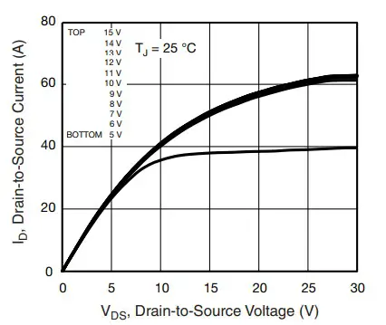
Fig. 1 – Typical Output Characteristics
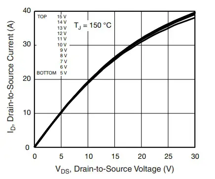
Fig. 2 – Typical Output Characteristics
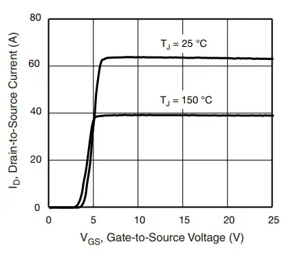
Fig. 3 – Typical Transfer Characteristics
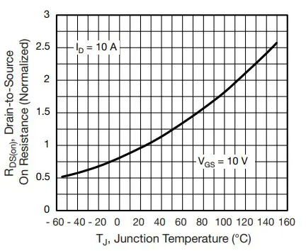
Fig. 4 – Normalized On-Resistance vs. Temperature
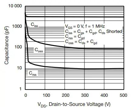
Fig. 5 – Typical Capacitance vs. Drain-to-Source Voltage
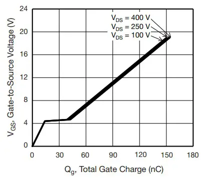
Fig. 6 – Typical Gate Charge vs. Gate-to-Source Voltage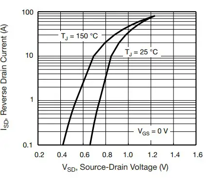
Fig. 7 – Typical Source-Drain Diode Forward Voltage
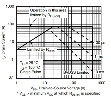
Fig. 7 – Typical Source-Drain Diode Forward Voltage
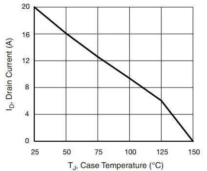
Fig. 8 – Maximum Safe Operating Area
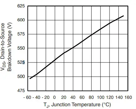
Fig. 9 – Maximum Drain Current vs. Case Temperature
Fig. 10 – Temperature vs. Drain-to-Source Voltage
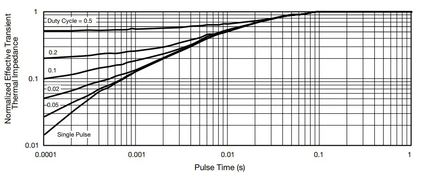
Fig. 11 – Normalized Thermal Transient Impedance, Junction-to-Case
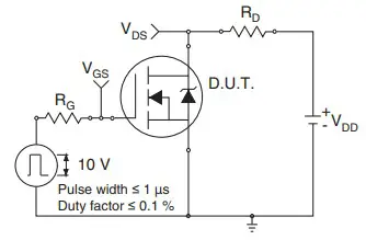
Fig. 12 – Switching Time Test Circuit
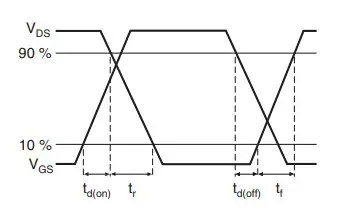
Fig. 13 – Switching Time Waveforms
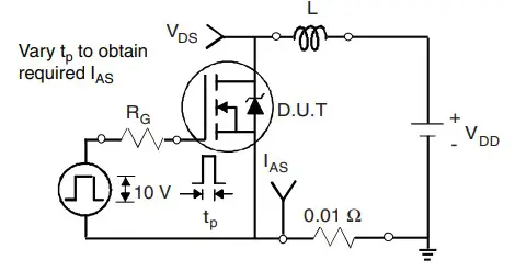
Fig. 15 – Unclamped Inductive Waveforms
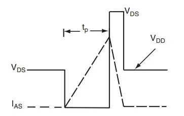
Fig. 16 – Basic Gate Charge Waveform
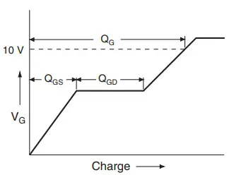
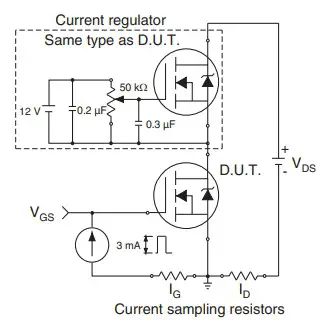
Fig. 17 – Gate Charge Test Circuit
Peak Diode Recovery dV/dt Test Circuit
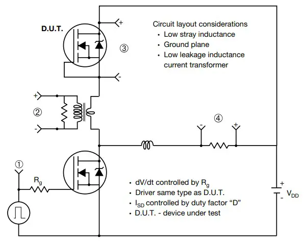
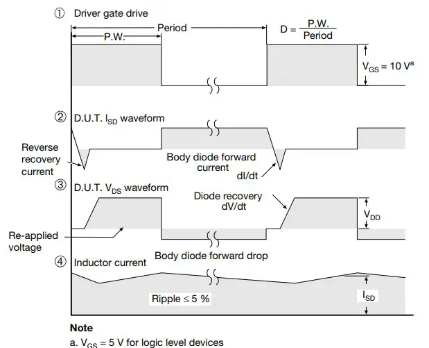
Fig. 18 – For N-Channel
Vishay Siliconix maintains worldwide manufacturing capability. Products may be manufactured at one of several qualified locations. Reliability data for Silicon
Technology and Package Reliability represent a composite of all qualified locations. For related documents such as package/tape drawings, part marking, and reliability data, see www.vishay.com/ppg?91502.
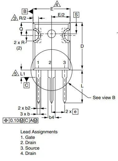
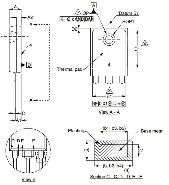
TO-247AC (High Voltage)
VERSION 1: FACILITY CODE = 9
| MILLIMETERS | |||
| DIM. | MIN. | MAX. | NOTES |
| A | 4.83 | 5.21 | |
| A1 | 2.29 | 2.55 | |
| A2 | 1.50 | 2.49 | |
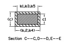
| b | 1.12 | 1.33 | |
| b1 | 1.12 | 1.28 | |
| b2 | 1.91 | 2.39 | 6 |
| b3 | 1.91 | 2.34 | |
| b4 | 2.87 | 3.22 | 6, 8 |
| b5 | 2.87 | 3.18 | |
| c | 0.55 | 0.69 | 6 |
| c1 | 0.55 | 0.65 | |
| D | 20.40 | 20.70 | 4 |
| MILLIMETERS | |||
| DIM. | MIN. | MAX. | NOTES |
| D1 | 16.25 | 16.85 | 5 |
| D2 | 0.56 | 0.76 | |
| E | 15.50 | 15.87 | 4 |
| E1 | 13.46 | 14.16 | 5 |
| E2 | 4.52 | 5.49 | 3 |
| e | 5.44 BSC | ||
| L | 14.90 | 15.40 | |
| L1 | 3.96 | 4.16 | 6 |
| Ø P | 3.56 | 3.65 | 7 |
| Ø P1 | 7.19 ref. | ||
| Q | 5.31 | 5.69 | |
| S | 5.54 | 5.74 | |
Notes
- Dimensioning and tolerancing per ASME Y14.5M-1994
- Contour of slot optional
- Dimension D and E do not include mold flash. Mold flash shall not exceed 0.127 mm (0.005″) per side. These dimensions are measured at the outermost extremes of the plastic body
- Thermal pad contour optional with dimensions D1 and E1
- Lead finish uncontrolled in L1
- Ø P to have a maximum draft angle of 1.5 to the top of the part with a maximum hole diameter of 3.91 mm (0.154″)
- Outline conforms to JEDEC outline TO-247 with exception of dimension c
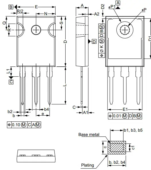
VERSION 2: FACILITY CODE = Y
| MILLIMETERS | |||
| DIM. | MIN. | MAX. | NOTES |
| A | 4.58 | 5.31 | |
| A1 | 2.21 | 2.59 | |
| A2 | 1.17 | 2.49 | |
| b | 0.99 | 1.40 | |
| b1 | 0.99 | 1.35 | |
| b2 | 1.53 | 2.39 | |
| b3 | 1.65 | 2.37 | |
| b4 | 2.42 | 3.43 | |
| b5 | 2.59 | 3.38 | |
| c | 0.38 | 0.86 | |
| c1 | 0.38 | 0.76 | |
| D | 19.71 | 20.82 | |
| D1 | 13.08 | – | |
| MILLIMETERS | |||
| DIM. | MIN. | MAX. | NOTES |
| D2 | 0.51 | 1.30 | |
| E | 15.29 | 15.87 | |
| E1 | 13.72 | – | |
| e | 5.46 BSC | ||
| Ø k | 0.254 | ||
| L | 14.20 | 16.25 | |
| L1 | 3.71 | 4.29 | |
| Ø P | 3.51 | 3.66 | |
| Ø P1 | – | 7.39 | |
| Q | 5.31 | 5.69 | |
| R | 4.52 | 5.49 | |
| S | 5.51 BSC | ||
Notes
- Dimensioning and tolerancing per ASME Y14.5M-1994
- Contour of slot optional
- Dimension D and E do not include mold flash. Mold flash shall not exceed 0.127 mm (0.005″) per side. These dimensions are measured at the outermost extremes of the plastic body
- Thermal pad contour optional with dimensions D1 and E1
- Lead finish uncontrolled in L1
- Ø P to have a maximum draft angle of 1.5 to the top of the part with a maximum hole diameter of 3.91 mm (0.154″)
- Outline conforms to JEDEC outline TO-247 with exception of dimension c
VERSION 3: FACILITY CODE = N
| MILLIMETERS | MILLIMETERS | |||||
| DIM. | MIN. | MAX. | DIM. | MIN. | MAX. | |
| A | 4.65 | 5.31 | D2 | 0.51 | 1.35 | |
| A1 | 2.21 | 2.59 | E | 15.29 | 15.87 | |
| A2 | 1.17 | 1.37 | E1 | 13.46 | – | |
| b | 0.99 | 1.40 | e | 5.46 BSC | ||
| b1 | 0.99 | 1.35 | k | 0.254 | ||
| b2 | 1.65 | 2.39 | L | 14.20 | 16.10 | |
| b3 | 1.65 | 2.34 | L1 | 3.71 | 4.29 | |
| b4 | 2.59 | 3.43 | N | 7.62 BSC | ||
| b5 | 2.59 | 3.38 | P | 3.56 | 3.66 | |
| c | 0.38 | 0.89 | P1 | – | 7.39 | |
| c1 | 0.38 | 0.84 | Q | 5.31 | 5.69 | |
| D | 19.71 | 20.70 | R | 4.52 | 5.49 | |
| D1 | 13.08 | – | S | 5.51 BSC | ||
| ECN: E20-0545-Rev. F, 19-Oct-2020 DWG: 5971 | ||||||
Notes
- Dimensioning and tolerancing per ASME Y14.5M-1994
- Contour of slot optional
- Dimension D and E do not include mold flash. Mold flash shall not exceed 0.127 mm (0.005″) per side. These dimensions are measured at the outermost extremes of the plastic body
- Thermal pad contour optional with dimensions D1 and E1
- Lead finish uncontrolled in L1
- Ø P to have a maximum draft angle of 1.5 to the top of the part with a maximum hole diameter of 3.91 mm (0.154″)
Disclaimer
ALL PRODUCT, PRODUCT SPECIFICATIONS AND DATA ARE SUBJECT TO CHANGE WITHOUT NOTICE TO IMPROVE RELIABILITY, FUNCTION OR DESIGN OR OTHERWISE.
Vishay Intertechnology, Inc., its affiliates, agents, and employees, and all persons acting on its or their behalf (collectively, “Vishay”), disclaim any and all liability for any errors, inaccuracies or incompleteness contained in any datasheet or in any other disclosure relating to any product.
Vishay makes no warranty, representation or guarantee regarding the suitability of the products for any particular purpose or the continuing production of any product. To the maximum extent permitted by applicable law, Vishay disclaims (i) any and all liability arising out of the application or use of any product, (ii) any and all liability, including without limitation special, consequential or incidental damages, and (iii) any and all implied warranties, including warranties of fitness for particular purpose, non-infringement and merchantability.
Statements regarding the suitability of products for certain types of applications are based on Vishay’s knowledge of typical requirements that are often placed on Vishay products in generic applications. Such statements are not binding statements about the suitability of products for a particular application. It is the customer’s responsibility to validate that a particular product with the properties described in the product specification is suitable for use in a particular application. Parameters provided in datasheets and / or specifications may vary in different applications and performance may vary over time. All operating parameters, including typical parameters, must be validated for each customer application by the customer’s technical experts. Product specifications do not expand or otherwise modify Vishay’s terms and conditions of purchase, including but not limited to the warranty expressed therein.
Hyperlinks included in this datasheet may direct users to third-party websites. These links are provided as a convenience and for informational purposes only. Inclusion of these hyperlinks does not constitute an endorsement or an approval by Vishay of any of the products, services or opinions of the corporation, organization or individual associated with the third-party website. Vishay disclaims any and all liability and bears no responsibility for the accuracy, legality or content of the third-party website or for that of subsequent links.
Except as expressly indicated in writing, Vishay products are not designed for use in medical, life-saving, or life-sustaining applications or for any other application in which the failure of the Vishay product could result in personal injury or death. Customers using or selling Vishay products not expressly indicated for use in such applications do so at their own risk. Please contact authorized Vishay personnel to obtain written terms and conditions regarding products designed for such applications.
No license, express or implied, by estoppel or otherwise, to any intellectual property rights is granted by this document or by any conduct of Vishay. Product names and markings noted herein may be trademarks of their respective owners.


