![]() life.augmented
life.augmented
UM1672
User manual
SPC56B-DIS discovery board
Introduction
This document describes the hardware architecture of the board, how to configure the jumpers and to enable specific functions.
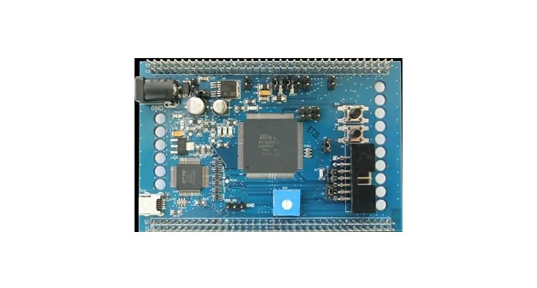
SPC56B-DIS discovery board with SPC560B54L5
SPC56B-DIS discovery board
The SPC56B-DIS discovery board is an evaluation tool supporting STMicroelectronics SPC56 B line microcontrollers. The evaluation board allows full access to all CPUs I/O signals and to peripherals.
Figure 1. SPC56B-DIS discovery board with SPC560B54L5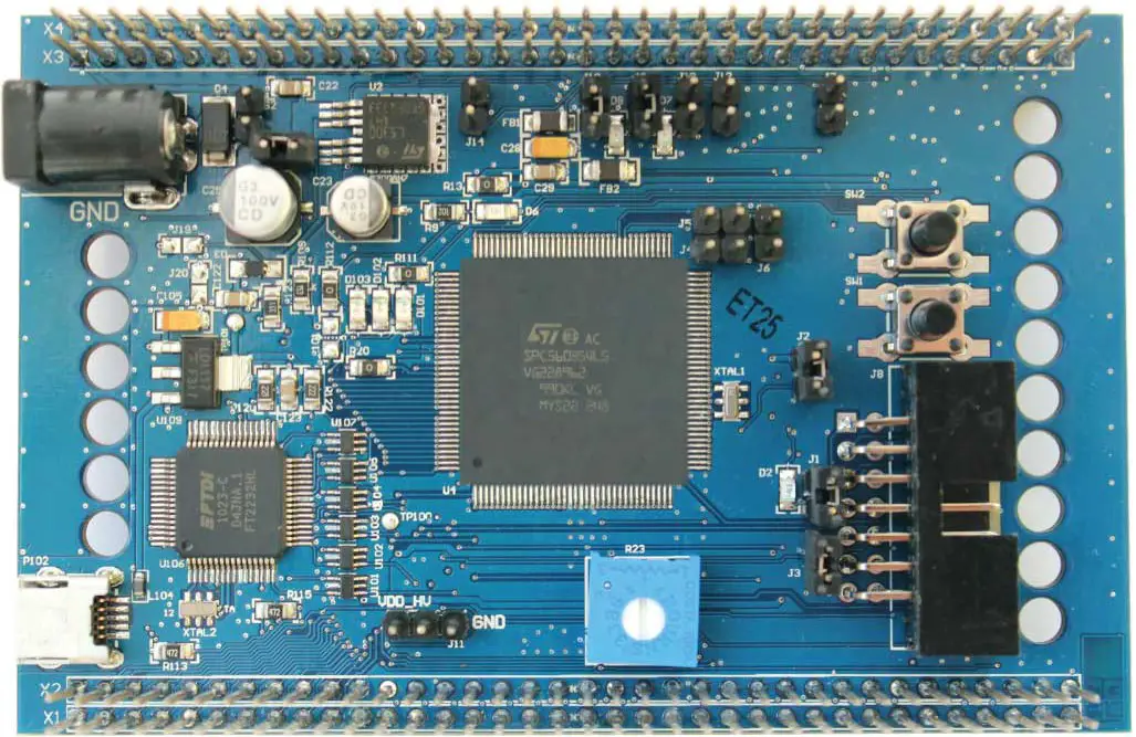
The SPC56 B line is STMicroelectronics state of the art MCU based on 32-bit microcontrollers Power Architecture Cores specifically addressing all Automotive Applications but as well suitable for industrial safety oriented applications. Such line is optimized for Body applications as Body Control Modules, Door Modules, Seat controls, HVAC, Comfort Modules, Security Access and they are suitable for ASIL B/SIL requirements.
SPC56B-DIS discovery board is supported by a specific application project inside SPC5Studio (a visual integrated software development environment to easily develop software for SPC56 MCU’s), that embeds micro start-up routines, I/O mapping and a simple test codes SPC5Studio that is available download www.st.com/spc5studio.
The PCB, the components and all HW parts meet requirements of the applicable RoHS directives.
Debug interface
The microcontroller can be debugged using:
- JTAG standard 14 pins interface, for using external debugger tools
- USB mini-B, through the PLS debugger integrated on board
Microcontroller I/Os
All microcontroller IOs are available on the two 2 x 36 headers with exception of JTAG, TCK, TMS, TDI, TDO, XTAL, EXTAL and VDD_LV pins.
Hardware overview
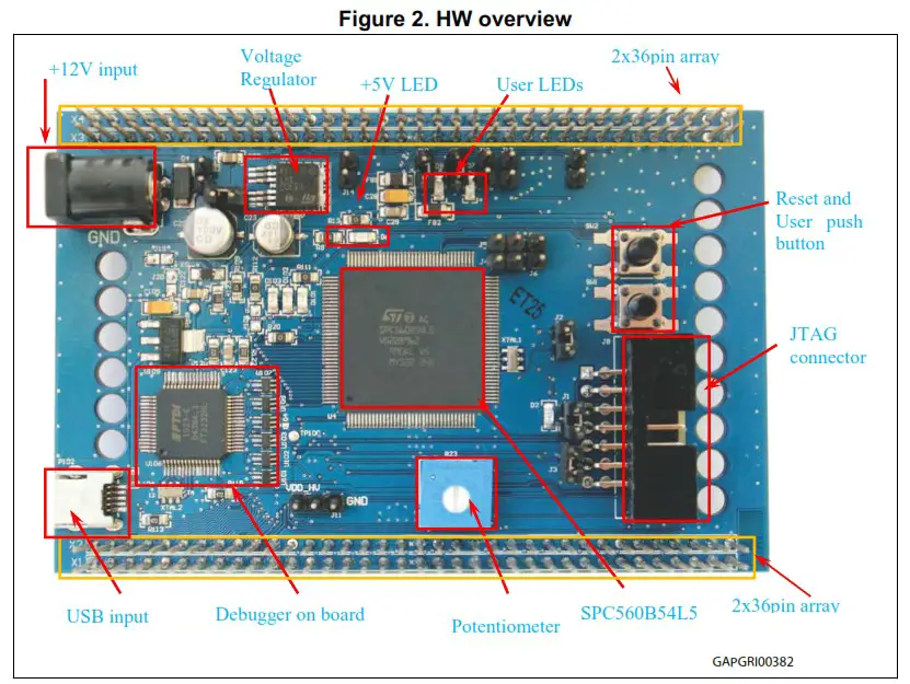
Power supply
The discovery board allows wide supply configurations, such as 12 V (external PSU) or 5 V (USB supply).
12 V DC power supply
12 V voltage can be used to supply the board(a)using the PSU output barrel connector (+12 V) or directly from 2×36 headers.
The PSU connector shall be center positive with 2.1 mm inner diameters.
The diode D4 protects the boards against the battery reverse connection. The jumpers S1 and S2 allow choosing the desired 12 V supply. Table 1 depicts the jumper configuration:
a. If the board is supplied with +12 V, the SMD solder jumpers J19 and J20 can be left opened.
Table 1. +12 V Supply configuration, S1 and S2 jumpers configuration
| S1 | S2 | +12 V Supply configuration |
| OPEN | OPEN | The board is not supplied with 12 V |
| CLOSE | OPEN | The board is supplied by the external PSU |
| CLOSE | CLOSE(1) | The discovery board supplies the daughter board (+12 V connected to the discovery board) or the daughters supplies the discovery (+12 V connected to the daughter board) (2) |
| OPEN | CLOSE | Not used |
- No supply voltage has to be connected to the daughter board.
- Only one of these HW configurations is allowed.
The jumper S1 can be used as switch to turn on and off the board.
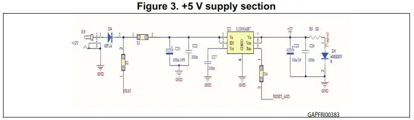
A linear regulator is used to generate +5 VDC needed for the microcontroller. D4 (green LED) is connected to voltage regulator output for revealing 5 V presence.
Supply from USB port
The board can be fed using the +5 V from the USB cable. To enable this function both jumpers J19 and J20 have to be closed and the PSU plug can be removed, together with S1 and S2 jumpers.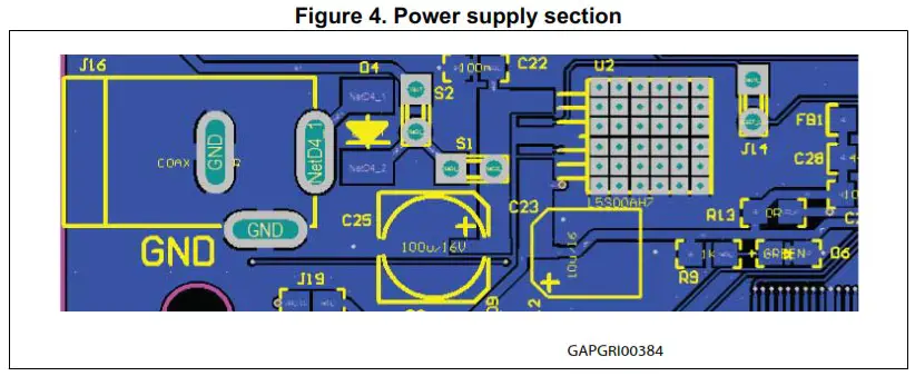
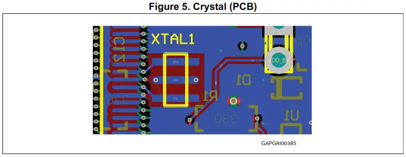
Crystal oscillator
The SPC56B-DIS board could be populated either with 8 or 16 MHz crystal to clock the SPC560B54L5.
Default configuration is with 16 MHz crystal.
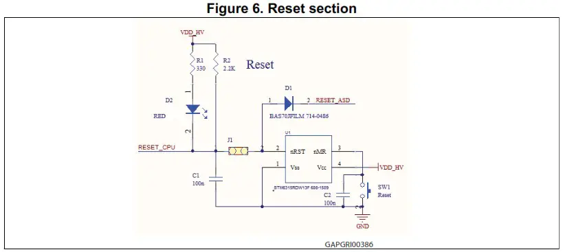
Reset section
In order to generate a clean reset signal for the microcontroller, STM6315RDW13F is used. SW1 button triggers such device generating a reset signal.
D8 is powered on as soon as reset pulse is generated.
The reset signal can be propagated to the on board linear voltage regulator via RESET_ASD line closing the jumper J14 (see Figure 3: +5 V supply section).
Programming and debug
The microcontroller in the discovery board can be programmed and debugged using two methods(b):
- Staport wndard JTAG connector (male 2×7 100mil – 90°)
- USB with integrated debugger.
A further configuration in addition to the previous ones allows to configure the board as a standalone PLS adapter; in this case, the JTAG connector has to be connected to the target board adding a passive male-female 2×7 pin adaptor.
JTAG connector
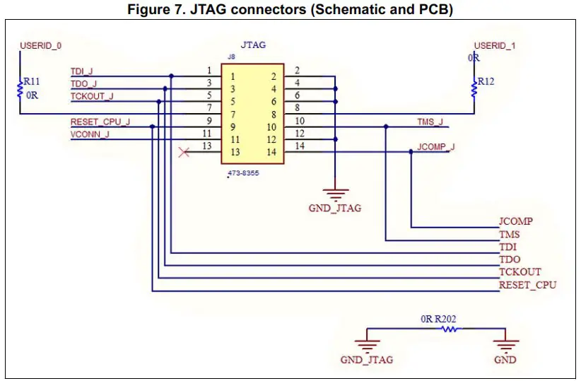
Table 2. JTAG connector (pin out)
| Pin num. | Name | Pin num. | Name |
| 1 | TDI | 2 | GND |
| 3 | TDO | 4 | GND |
| 5 | TCK | 6 | GND |
| 7 | EVTI | 8 | NC |
| 9 | RESET | 10 | TMS |
| 11 | VDDE7 | 12 | GND |
| 13 | RDY | 14 | JCOMP |
b. A single configuration can be enabled at one time. The jumpers setting to enable the configuration is described in the paragraph Section 2.4.3: Board configured as PLS adapter.
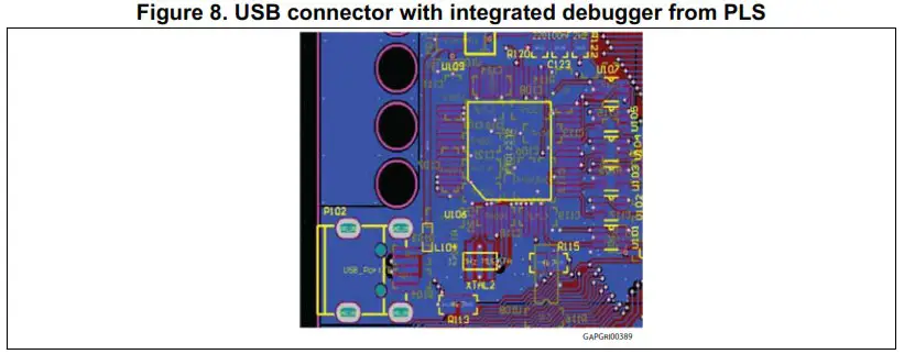
USB with integrated debugger from PLS (default configuration)
The integrated debugger, based on the device FTDI2232H and UDE PLS software, allows the user to build, run and debug the software applications. The SPC56B-DIS discovery kit includes a full-featured, perpetual code-limited (128 Kbytes) PLS software license; the debugger serial number is reported on a label applied on the bottom side of the board.
To download the debugger software and to activate license go to the PLS website.
The integrated debugger is accessible via ST’s free integrated development environment, SPC5Studio (www.st.com/spc5studio).
Board configured as PLS adapter
The discovery board can be configured to work as standalone PLS adapter, configuring jumpers as described below (see Table 3: Programming and debug – Jumper setting). The board serial number is reported in a label on the board. A passive adapter can be added to converter from male to female the 2 x 7 JTAG port soldered on the board. The 3.3 V or 5 V compatibility is achieved by using level shifters array.
HW configuration
In order to enable one of the previous described functionalities, the board has to be properly set. The USB integrated debugger is the default configuration. Table 3 shows how to configure the jumpers also to enable the board as PLS adapter..:
Table 3. Programming and debug – Jumper setting
| Jumper name | JTAG | USB (Integrated debugger) | PLS Adapter |
| J101 | Open | Close | Close |
| J102 | Open | Close | Close |
| J103 | Open | Close | Close |
| J105 | Open | Close | Close |
| J109 | Open | Close | Close |
| J110 | Open | Close | Close |
| J111 | Open | Close | Close |
| J114 | Open | Close | Close |
| J19 | Open | Open | Close |
| J20(1) | Close | Close | Close |
| S1(2) | Close | Close | Open |
| S2(3) | Open | Open | Open |
| J1 | Close | Close | Close |
| J2 | Close | Close | Close |
| J3 | Close | Close | Close |
- J20 connect the GND of the board to the GND of the USB input. This jumper should be removed when the USB section must be electrically insulated
- S1 is used as power switch; if S1 is left open, the 12V form external source does not supply the board
- If S2 is present and the 12V supply comes from the daughters boards, J16 must be left unconnected (no external PSU must be powered and connected).
USB and Graphic User Interface (GUI)
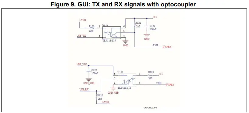
One of the two FTDI2232 channels has been configured for implementing a serial communication between PC USB and microcontroller UART, both for serial booting and for controlling the microcontroller using a dedicated GUI.
The USB section (serial communication) is electrical insulated with respect to all the circuitry adding opto-couplers in series to the path of TX and SX signals, see Figure 9: GUI: TX and RX signals with optocoupler .
User I/O pins
Some microcontroller GPIOs are dedicated for user purpose. Here below details about each group.
User LEDs
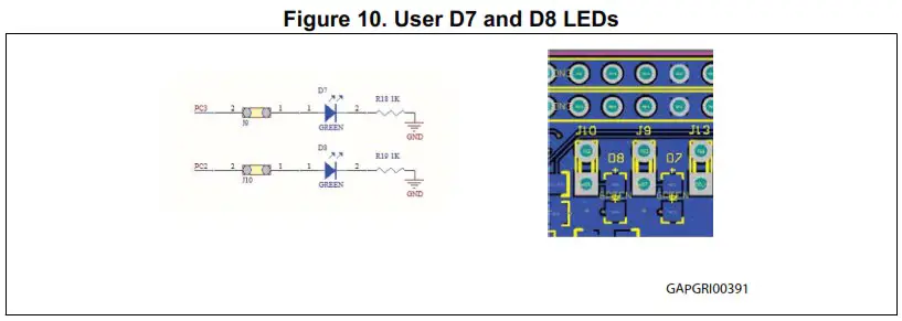
The LEDs D7 and D8 are available for user purpose; the jumpers J9, J10 connect the 2 LEDs to the microcontroller I/O PC3 and PC2 respectively. The HW connection is reported in Figure 10: User D7 and D8 LEDs.
A push button is connected to GPIO PA11. The pin is connected to High level by a 10 k pull-up resistor and it is set to Low (GND) when the button is pushed; a low pass filter has been added to reduce the noise and clean spurious signals.

User I/O pins
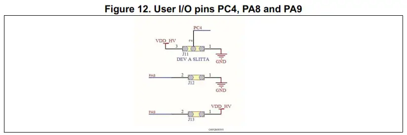
Pin PC4 can be set to Low or High configuring J11.
Boot configuration
It is possible to reprogram microcontroller internal Flash programming to use Boot Assist Mode (BAM) via SCI. The pins PA8 and PA9, (see Figure 12: User I/O pins PC4, PA8 and PA9) have to be configured to enable the BAM functionality as following:
- FABM (PA9) has to be connected to VDD_HV to enable serial boot (J13 jumper closed).
- ABS (PA8) has to be physically grounded to flash via SCI (J12 jumper closed).
If the BAM function is not used, these pins can be configured as normal I/O according to the functions reported in the datasheet (see Section Appendix B: Reference documents).
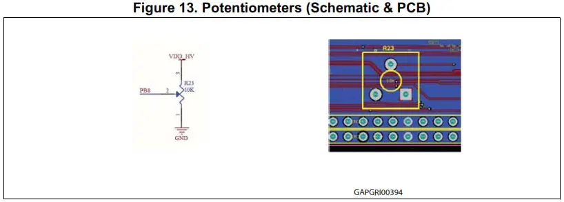
ADC input
A trimmer connected to the microcontroller PB8 input allows the user to check ADC. The analog input voltage range is 0V ÷ VDD_HV.
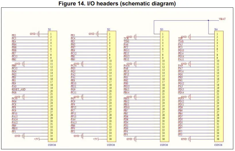
Daughter board connector and I/O headers
The I/O microcontroller pins are connected to a double 2 x 36 pin array (connectors X1-X2 and X3-X4).
Table 4. I/O headers
| Pin number | X*1 | X2 | X3 | X4 |
| 1 | GND | GND | VBAT | VBAT |
| 2 | PE[2] | PE[3] | GND | GND |
| 3 | PC[5] | PC[4] | TCK | TDI |
| PE[4] | PE[5] | TDO | TMS | |
| 5 | PH[4] | PH[5] | PA[6] | PA[5] |
| 6 | PH[6] | PH[7] | PC[2] | PC[3] |
| 7 | PH[8] | PE[6] | PG[11] | PG[10] |
| 8 | PE[7] | PC[12] | PE[15] | PE[14] |
| 9 | PC[13] | PB[1] | PG[15] | PG[14] |
| 10 | PB[2] | PB[3] | PE[12] | PA[11] |
| 11 | GND | GND | GND | GND |
| 12 | PB[0] | PC[14] | PA[10] | PA[9] |
| 13 | PC[15] | PG[5] | PA[8] | PA[7] |
| 14 | PG[4] | PG[3] | PE[13] | PF[14] |
| 15 | PG[2] | PA[2] | PF[15] | PG[0] |
| 16 | PE[0] | PA[1] | PG[1] | PH[3] |
| 17 | PE[1] | PE[8] | PH[2] | PH[1] |
| 18 | PE[9] | PE[10] | PH[0] | PG[12] |
| 19 | PA[0] | PE[11] | PG[13] | PA[3] |
| 20 | Reset ASD | PG[9] | PB[15] | PD[15] |
| 21 | PG[8] | PC[11] | PB[14] | PD[14] |
| 22 | GND | GND | GND | GND |
| 23 | PC[10] | PG[7] | PB[13] | PD[13] |
| 24 | PG[6] | PC[9] | PB[12] | PD[12] |
| 25 | PC[8] | PF[9] | PB[11] | PD[11] |
| 26 | PF[8] | PF[12] | PD[10] | PD[9] |
| 27 | PC[6] | PC[7] | PB[7] | PB[6] |
| 28 | PF[10] | PF[11] | PB[5] | PB[4] |
| 29 | PA[15] | PF[13] | PD[8] | PD[7] |
| 30 | PA[14] | PA[4] | PD[6] | PD[5] |
| 31 | PA[12] | PA[13] | PD[4] | PD[3] |
| 32 | PB[9] | PB[8] | PD[2] | PD[1] |
| 33 | PB[10] | PF[0] | PD[0] | PF[7] |
| 34 | PF[1] | PF[2] | PF[6] | PF[5] |
| 35 | GND | GND | PF[4] | PF[3] |
| 36 | 5V | 5V | GND | GND |
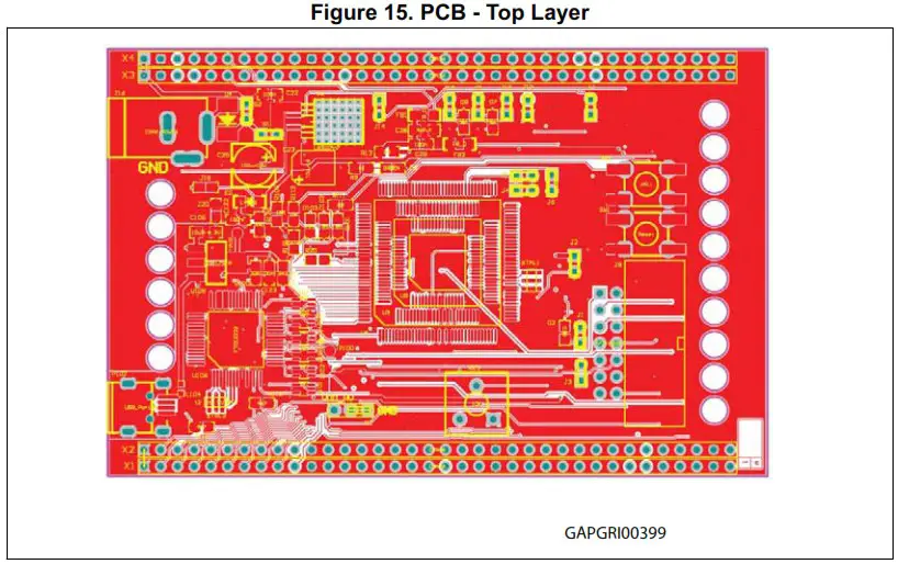
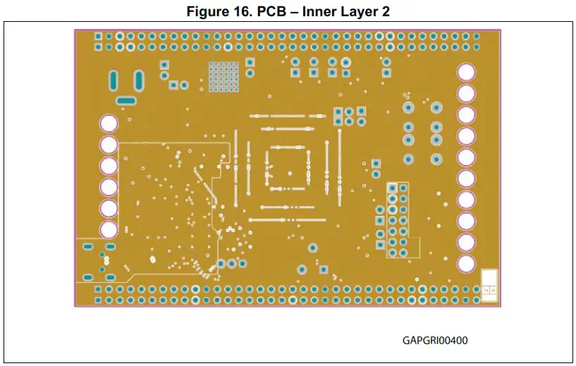
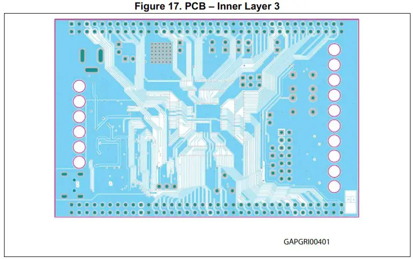
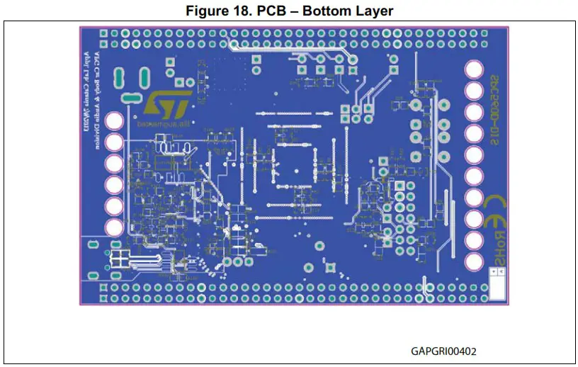
PCB Layout
Appendix A General handling precautions
The following precautions are recommended when using the SPC56B-DIS, discovery board:
- Do not modify or manipulate the board when the external PSU supply is powered and connected to the board.
- Do not open and modify the PSU. Use AC plug adaptor if the main socket is not compatible with the PSU plug.
- Do not supply the board with a DC source higher than 12 V.
- Any equipment or tool used for any manipulation of the semiconductor devices or board modification should be shielded and connected to ground.
- The connectors and cables should be plugged and removed when the board is not supplied.
- It is recommended to use antistatic tools.
Appendix B Reference documents
32-bit MCU family built on the Power Architecture® for automotive body electronics applications (Datasheet, Doc ID 15131).
Revision history
Table 5. Document revision history
| Date | Revision | Changes |
| 04-Nov-13 | 1 | Initial release. |
| 14-Dec-20 | 2 | Updated Table 4: I/O headers. |
IMPORTANT NOTICE – PLEASE READ CAREFULLY
STMicroelectronics NV and its subsidiaries (“ST”) reserve the right to make changes, corrections, enhancements, modifications, and improvements to ST products and/or to this document at any time without notice. Purchasers should obtain the latest relevant information on ST products before placing orders. ST products are sold pursuant to ST’s terms and conditions of sale in place at the time of order acknowledgement.
Purchasers are solely responsible for the choice, selection, and use of ST products and ST assumes no liability for application assistance or the design of Purchasers’ products.
No license, express or implied, to any intellectual property right is granted by ST herein.
Resale of ST products with provisions different from the information set forth herein shall void any warranty granted by ST for such product.
ST and the ST logo are trademarks of ST. For additional information about ST trademarks, please refer to www.st.com/trademarks. All other product or service names are the property of their respective owners.
Information in this document supersedes and replaces information previously supplied in any prior versions of this document.
© 2020 STMicroelectronics – All rights reserved
UM1672 Rev 2
Downloaded from Arrow.com.


