![]() UM2255
UM2255
User manual
SPC58NG-DISP discovery board
Introduction
The SPC58NG-DISP discovery board is the hardware platform to evaluate and develop applications with the SPC58NG84E7 microcontroller at a budget price.
This document describes the hardware architecture of the board and how it is possible to enable specific functions.
UM2255 – Rev 3 – February 2021
For further information contact your local STMicroelectronics sales office.
www.st.com
SPC58NG-DISP
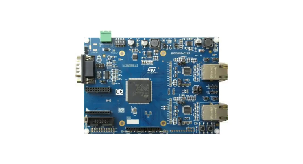
Figure 1. SPC58NG-DISP
The SPC58NG-DISP discovery board is based on the microcontroller SPC58NG84E7, a high-performance e200z4d triple-core 32-bit Power Architecture® technology CPU, 6 MB Flash with HSM cryptography in an eTQFP176 package.
The several interfaces include GPI/O’s, peripherals such as DSPI, LINFlexD (LIN and UART), FlexRay, M_CAN ISO CAN-FD, and two ethernet ports make the SPC570S- DISP an excellent starter kit for the customer to quickly evaluate the microcontroller as well as to develop and debug application.
Free ready-to-run application firmware examples are available inside the SPC5Studio web page (www.st.com/spc5studio) to support quick evaluation and development.
The PCB, the components, and all HW parts assembled in this board meet the requirements of the applicable RoHS directives.
I/O interface and connectors
- 2 ethernet ports 100BASE-TX
- 1 CAN FD port with DB9 connector
- 1 CAN + 1 LIN/UART +1 SPI
- 2 FlexRay channels
- JTAG (header 2 x 7 pin)
- 4 LED’s user
- 4 DIP switches
- 2 user pushbuttons
- 12 V DC power supply (external PSU)
- RESET push button
- 40 MHz crystal
- Option: LCD TFT display (320 x 240) with touch screen
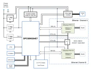
SPC58NG-DISP block diagram
Figure 2. SPC58NG-DISP block diagram
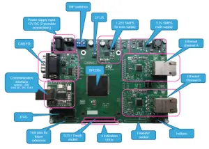
Hardware overview
Figure 3. SPC58NG-DISP: HW overview
Power supply section
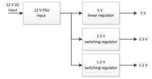
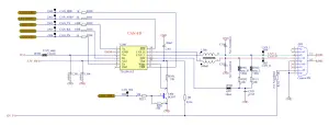
Figure 4 shows the PSU block diagram.
The DC input source is 12 V and the three voltage regulators generate 5 V, 3.3 V and 1.2 V supply voltages.
The LEDs D1, D2, and D3 are used to monitor the output of each voltage regulator as well as the test points J2, J3, J5, and J13 to allow measuring the voltage levels 12 V, 5 V, 3.3 V, and 1.2 V respectively.
Power supply – jumper configuration
U2 provides 3.3 V output voltage used to supply the VDD_HV pins. The test point J5 can be used to monitor the VDD_HV supply voltage level.
The VDD_LV pin can be supplied using an internal regulator and a ballast BJT or providing the supply by using an external source. In the default configuration, the jumpers are set to supply VDD_LV with the external source (U3) The VDD_LV power supply configuration can be easily configured setting the soldering jumpers as summarized in the table here below.
Table 1. Power supply – jumper configuration
Configuration | JP100 | JP101 | JP102 | R100 |
| External supply (default) | Open | 1-3 | 1-2 | Removed |
| Internal regulator + external BJT | Closed | 1-2 | 1-3 | Assembled |
Figure 5. Microcontroller power supply configuration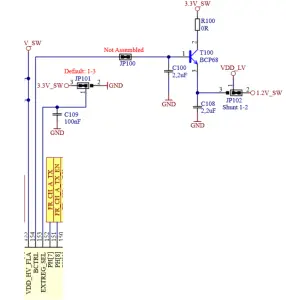
Microcontroller section
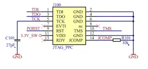
Programmer/debugger JTAG port
A standard 14 pin JTAG port is available for programming and debugging (Figure 6).
User LEDs and user buttons
In the board, the following functions are available:
- 4 LEDs (Figure 7)
- 2 push buttons (Figure 8)
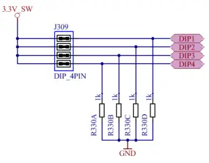
- 4 DIP switches (Figure 9)
Figure 7. User LEDs

Figure 8. User push buttons
Figure 9. Dip switches
Ethernet configuration
Ethernet MII / RMII configuration
Table 2. Ethernet MII jumper configuration
Default configuration – MII | |
Jumper | Jumper setting |
JP205 | 1-2 |
| JP201 | 1-2 |
JP211 | 1-2 |
| JP209 | 1-2 |
JP210 | 1-2 |
| JP208 | 1-2 |
Table 3. Ethernet RMII jumper configuration
| Default configuration – RMII | |
Jumper | Jumper setting |
JP205 | 1-3 |
| JP201 | 1-3 |
JP211 | 1-3 |
| JP209 | 1-3 |
JP210 | 1-3 |
| JP208 | 1-3 |
X200 | Assembled |
| X203 | Assembled |
Ethernet PHY serial management
Table 4. Ethernet – Configuration for separated management
Configuration for separated management | |
MDC0, MDIO0 linked to ETH0 | |
MDC1, MDIO1 linked to ETH1 | |
JP203 | 1-2 |
| JP204 | 1-2 |
Table 5. Ethernet – Configuration for share management
Configuration for shared management | |
MDC0, MDIO0 linked to ETH0 and ETH1 | |
ETH0 = address 1 | |
ETH1 = address 3 | |
JP203 | 1-3 |
| JP204 | 1-3 |
CAN-FD
Figure 11 shows the CAN-FD section with the transceiver and the DB9 connector.
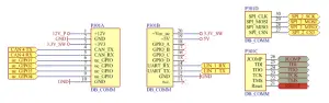
Communication daughter board socket
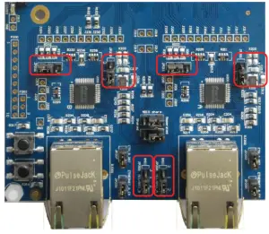
The functionality of SPC58NG-DISP increases the plugging of some additional daughter boards in the connectors P301, P301B, P301C, and P301D (see Figure 12).
Figure 12. Communication daughter board socket
Revision history
Table 6. Document revision history
| Date | Version | Changes |
| 31-Jul-2017 | 1 | Initial release. |
| 03-Sep-2018 | 2 | Updated Introduction. Minor text changes. |
| 18-Feb-2021 | 3 | Updated title on the cover page. Updated Section 3.1.1 Power supply – jumper configuration and moved from previous to the current position. Minor text changes. |
STMicroelectronics NV and its subsidiaries (“ST”) reserve the right to make changes, corrections, enhancements, modifications, and improvements to ST products and/or to this document at any time without notice. Purchasers should obtain the latest relevant information on ST products before placing orders. ST products are sold pursuant to ST’s terms and conditions of sale in place at the time of order acknowledgment.
Purchasers are solely responsible for the choice, selection, and use of ST products and ST assumes no liability for application assistance or the design of Purchasers’ products.
No license, express or implied, to any intellectual property right is granted by ST herein.
Resale of ST products with provisions different from the information set forth herein shall void any warranty granted by ST for such product.
ST and the ST logo are trademarks of ST. For additional information about ST trademarks, please refer to www.st.com/trademarks. All other product or service names are the property of their respective owners.
Information in this document supersedes and replaces information previously supplied in any prior versions of this document.
© 2021 STMicroelectronics – All rights reserved


