![]() SPC56L Discovery Evaluation Board
SPC56L Discovery Evaluation Board
User Manual
Introduction
This document describes how to configure the board and how to setup the I/O communication.
SPC56L-Discovery
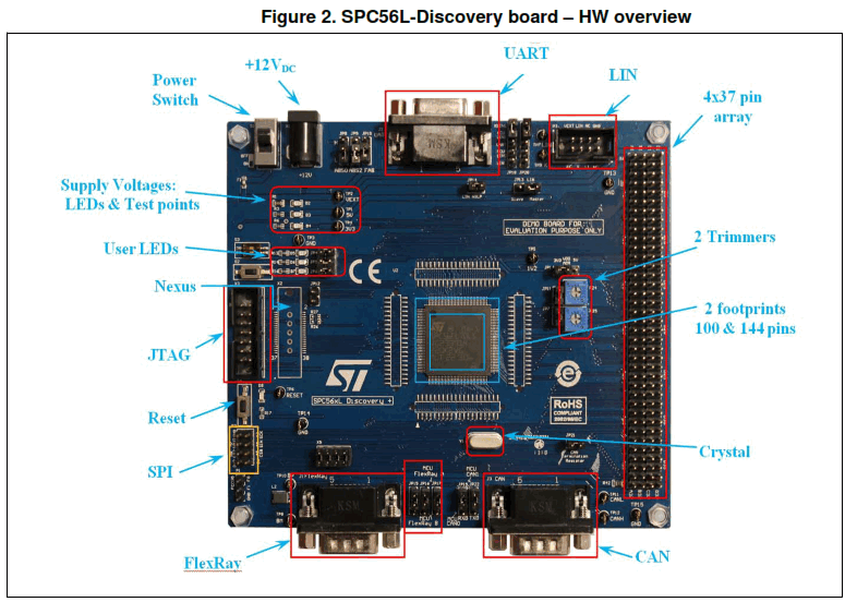
1.1SPC56L-Discovery evaluation board
The SPC56L-Discovery kit is an evaluation tool supporting STMicroelectronics SPC56xL microcontrollers. The evaluation board allows full access to all of the CPUs I/O ignals, and the peripherals such as CAN, FlexRay, UART, JTAG, K-Line, LIN.
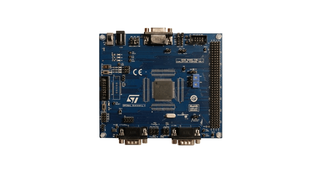
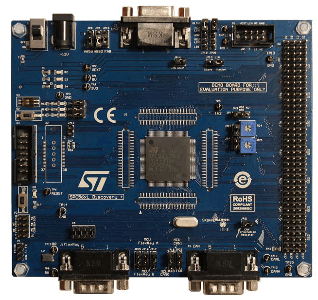
Figure 1. SPC56L-Discovery board with SPC56EL70L5
The content of hardware of SPC56L-Discovery consists of:
• SPC56L-Discovery kit board (Figure 1).
• Power Supply (Mains: 90-240 VAC – Output: 12 VDC).
The SPC56xL family is ST state of the art MCU based on 32-bit microcontrollers Power Architecture® Cores specifically addressing all Automotive Applications but as well uitable for industrial safety oriented applications. The SPC56xL devices are optimized for chassis & safety applications and suitable for ASIL D/SIL level 3 requirements. SPC56L-Discovery is supported by a specific Application Project inside SPC5Studio (a visual integrated software development environment to easily develop software for PC56 MCU’s), where micro start-up routine, I/O mapping and a simple test code has been already designed by STMicroelectronics experts. SPC5Studio is available for download www.st.com/spc5studio
SPC5Studio comes with HighTec GNU “C” compiler free fully featured trial 30 days trial version. An E2E Community is available on ST WEB: https://my.st.com/public/STe2ecommunities/mcu
The PCB, the components and all HW meet requirements of the applicable RoHS directives.
1.2 Debug interface
14 pin JTAG interface
38 pin High speed Nexus interface (Optional)
1.3 I/O interface and connectors
- PSU plug (+12 V)
- UART (DB9-female)
- CAN interface (DB9-male)
- FlexRay (DB9-male)
- LIN
- K-Line
- 4 x 37 headers
Hardware overview
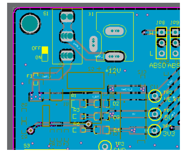
2.1 12 VDC power supply adapter
The 12 VDC voltage is used to supply the whole board including the microcontroller and the communication interface transceiver chips. The power supply is included in the it. The 12 V adapter can be supplied with mains 90÷240 VAC; the AC plug is the standard CEE 7/16 Europlug. The PSU output barrel connector (+12 VDC) is center positive power supply with 2.1/5.5 mm diameters.
2.2 +5 V and +3.3 V power supply sections
A dedicated DC-DC converter is used to generate +5 VDC. A linear low dropout regulator is used to generate +3.3 V. The switch S1 is used to turn on and turn off the oard. 3 LEDs (D2, D3 and D4) are connected to 12 V, +5 V and 3.3 V respectively.
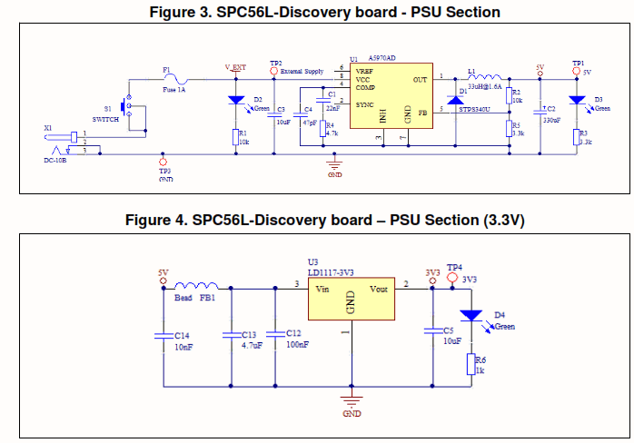
Three test points are available to measure the voltage levels: TP2=12V, TP1=5V, TP4=3V3 while TP3 is connected to GND F1 (1A) is a not resettable fuse.
Figure 5. SPC56L-Discovery board – +12 VDC supply
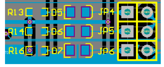
2.3 User LEDs
Three LEDs are available and can be configured by the user. The LEDs are D5, D6 and D7. Jumper JP4, JP5 and JP6 connect the LEDs to the microcontroller.
Y1 is a 40 MHz through-hole crystal. The crystal is plugged in a dedicated socket and it can be replaced without using a soldering station.
Figure 7. SPC56L-Discovery board – Crystal (PCB)
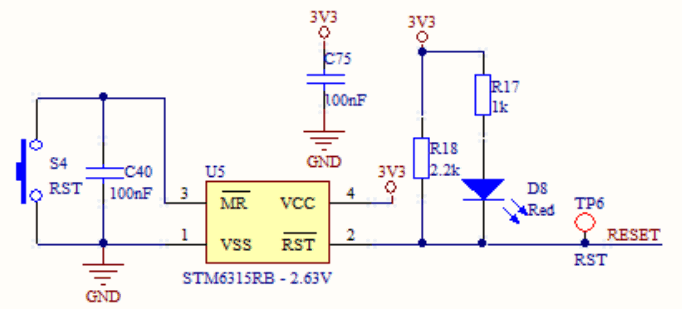
2.4 Reset
A reset section is present in the board. The resent signal is generated using the device STM6315RB when the button S4 is pushed; the LED D8 will be turned on when the eset pulse is generated.
Figure 8. SPC56L-Discovery board – Reset (PCB)
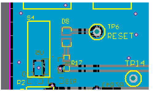
Figure 9. SPC56L-Discovery board – Reset (schematic)
2.5 JTAG connector
Figure 10. SPC56L-Discovery board – JTAG and Nexus connectors (PCB)
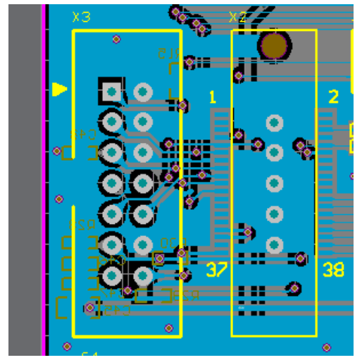
Figure 11. SPC56L-Discovery board – JTAG connector (Schematic)
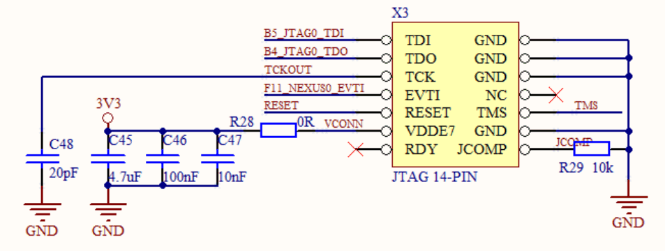
Table 1. SPC56L-Discovery board – JTAG connector (pin out)
| Pin number | Pin name | Pin number | Pin name |
| 1 | TDI | 2 | GND |
| 3 | TDO | 4 | GND |
| 5 | TCK | 6 | GND |
| 7 | EVTI | 8 | NC |
| 9 | RESET | 10 | TMS |
| 11 | VDDE7 | 12 | GND |
| 13 | RDY | 14 | JCOMP |
Figure 12. SPC56L-Discovery board – Nexus connector (Schematic)
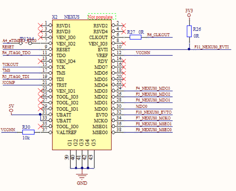
2.6High speed Nexus interface (Optional)
Figure 12 shows connector for Nexus interface for high-end development tools; (the PCB is shown in Figure 10).
Table 2. SPC56L-Discovery board – Nexus connector
| Pin number | Pin name | Pin number | Pin name |
| 1 | RSVD1 | 2 | RSVD2 |
| 3 | RSVD3 | 4 | RSVD4 |
| 5 | VEN_IO0 | 6 | CLKOUT |
| 7 | VEN_IO2 | 8 | VEN_IO3 |
| 9 | RESET | 10 | EVTI |
| 11 | TDO | 12 | VREF |
| 13 | VEN_IO4 | 14 | RDY |
| 15 | TCK | 16 | MDO7 |
| 17 | TMS | 18 | MDO6 |
| 19 | TDI | 20 | MDO5 |
| 21 | TRST | 22 | MDO4 |
| 23 | VEN_IO1 | 24 | MDO3 |
| 25 | TOOL_IO3 | 26 | MDO2 |
| 27 | TOOL_IO2 | 28 | MDO1 |
| 29 | TOOL_IO1 | 30 | MDO0 |
| 31 | UBATT | 32 | EVT0 |
| 33 | UBATT | 34 | MCKO |
| 35 | TOOL_IO0 | 36 | MSEO1 |
| 37 | VALTREF | 38 | MSEO0 |
2.7 SPI Connector
Figure 13. SPC56L-Discovery board – SPI connector (PCB)
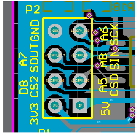
Figure 14. SPC56L-Discovery board – SPI connector (Schematic)
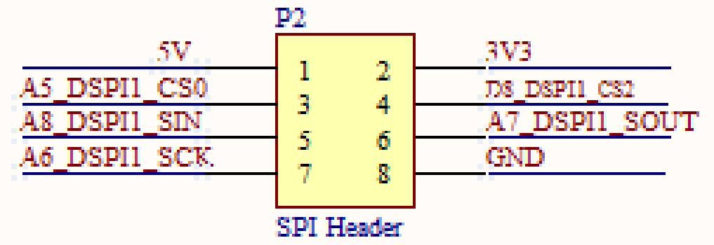
Table 3. SPC56L-Discovery board – SPI connector (pin out)
| Pin number | Pin name | Pin number | Pin name |
| 1 | +5V | 2 | +3.3V |
| 3 | CSO | 4 | CS2 |
| 5 | SIN | 6 | SOUT |
| 7 | SCK | 8 | GND |
2.8 High Speed CAN interface
The CAN module is integrated in SPC56L-Discovery board; CAN transceiver is AMIS-30663 which support high-speed CAN.
Regarding the CAN connector, the two basic CAN channels are located in a DB9 male connector and they can be selected with a jumper option (JP19 and JP20).
Figure 15. PC56L-Discovery board – High Speed CAN interface (PCB)
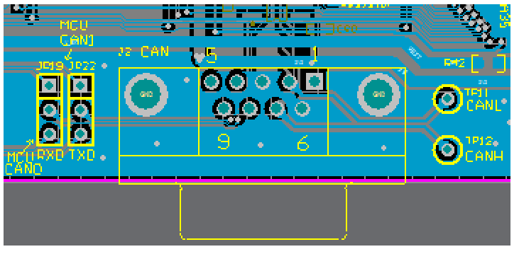
Figure 16. SPC56L-Discovery board – High Speed CAN interface (schematic)
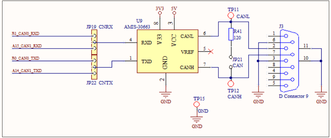
Jumper JP21 is used to set proper 120 Ω termination resistor for CAN bus; disconnect this jumper if unnecessary.
TP11 and TP12 are connected to the CANL and CANH respectively (pin 2 and pin 7 of the DB9 connector J3).
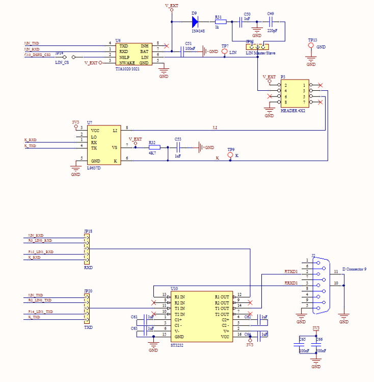
2.9 UART / LIN
Figure 17 and Figure 18 shows the hardware connection on evaluation board and the schematic diagram for the UART/LIN. ST232 is the bridge between RS232 DB9 female nterface and TX/RX signal of microcontroller; the L9637 is the ISO9141 interface chip.
In the microcontroller side, the user can set the JP18 and JP19 to configure UART or LIN.
Figure 17. SPC56L-Discovery board – UART / LIN (PCB)
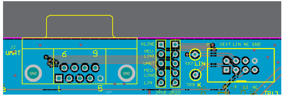
Figure 18. SPC56L-Discovery board – UART / LIN (schematic)
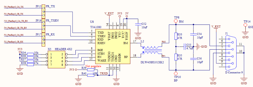
2.10 FlexRay
In the microcontroller side the user can configure the jumpers JP15, JP16 and JP7 allow to set channel A or B .
Figure 19. SPC56L-Discovery board – FlexRay (PCB)
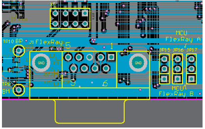
Figure 20. SPC56L-Discovery board – FlexRay (schematic)
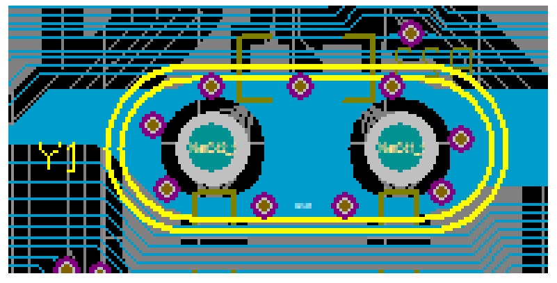
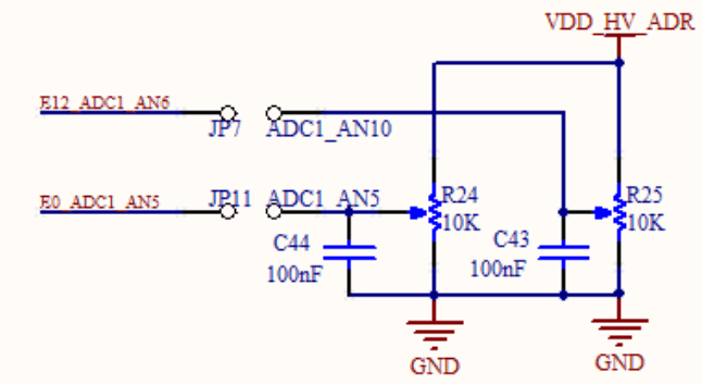
2.11 Potentiometers
There are two potentiometers on the board which allow user to feed a range of voltage values into the ADC input to evaluate the performance of ADC.
The analog voltage level (0~VDD_HV_ADRV) can be monitored if the jumper JP7 and/oJP11 are inserted; the digital value can be read from microcontroller.
Figure 21. SPC56L-Discovery board – Potentiometers (PCB)
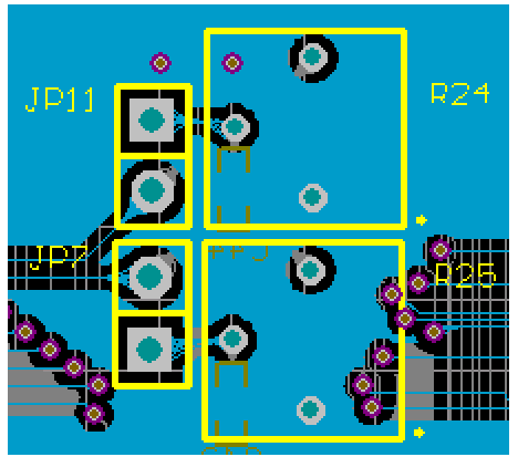
Figure 22. SPC56L-Discovery board – Potentiometers (schematic)
2.12 I/O header
The I/O microcontroller ins are connected to a 4×37 pin array (connector X6).
Figure 23. SPC56L-Discovery board – I/O header (schematic)
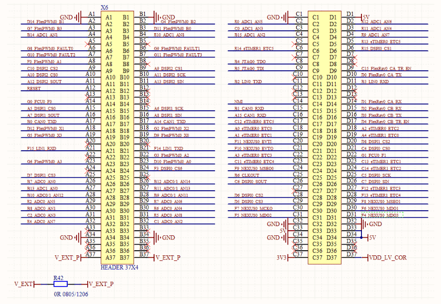
Table 4. SPC56L-Discovery board – I/O header (Table, part 1)
| X6 Pin | Port | Description | X6 Pin | Port | Description |
| A1 | GND | B1 | GND | ||
| A2 | D14 | FlexPWM0_B1 | B2 | G4 | FlexPWM0_B2 |
| A3 | G7 | FlexPWM0_B3 | B3 | D11 | FlexPWM0_B0 |
| A4 | B14 | ADC1_AN1 | B4 | E10 | ADC1_AN8 |
| A5 | NC | B5 | NC | ||
| A6 | G8 | FlexPWM0_FAULT0 | B6 | G9 | FlexPWM0_FAULT1 |
| A7 | G10 | FlexPWM0_FAULT2 | B7 | G11 | FlexPWM0_FAULT3 |
| A8 | F0 | FlexPWM0_A1 | B8 | NC | |
| A9 | C10 | DSPI2_CS2 | B9 | A9 | DSPI2_CS1 |
| A10 | A10 | DSPI2_CS0 | B10 | A11 | DSPI2_SCK |
| A11 | A12 | DSPI2_SOUT | B11 | A13 | DSPI2_SIN |
| A12 | RESET_B | RESET | B12 | NC | |
| A13 | NC | B13 | NC | ||
| A14 | G0 | FCU0_F0 | B14 | NC | |
| A15 | A5 | DSPI1_CS0 | B15 | A6 | DSPI1_SCK |
| A16 | A7 | DSPI1_SOUT | B16 | A8 | DSPI1_SIN |
| A17 | B0 | CAN0_TXD | B17 | A14 | CAN1_TXD |
| A18 | D12 | FlexPWM0_X1 | B18 | G2 | FlexPWM0_X2 |
| A19 | G5 | FlexPWM0_X3 | B19 | D9 | FlexPWM0_X0 |
| A20 | NC | B20 | NC | ||
| A21 | F15 | LIN1_RXD | B21 | F14 | LIN1_TXD |
| A22 | NC | B22 | G3 | FlexPWM0_A2 | |
| A23 | G6 | FlexPWM0_A3 | B23 | D10 | FlexPWM0_A0 |
| A24 | NC | B24 | F3 | DSPI0_CS6 | |
| A25 | D7 | DSPI1_CS3 | B25 | NC | |
| A26 | B7 | DC0_AN0 | B26 | B12 | ADC0/1_AN14 |
| A27 | B13 | ADC1_AN0 | B27 | B11 | ADC0/1_AN13 |
| A28 | B10 | ADC0/1_AN12 | B28 | B9 | ADC0/1_AN11 |
| A29 | E2 | ADC0_AN5 | B29 | E7 | ADC0_AN6 |
| A30 | B8 | ADC0_AN1 | B30 | E6 | ADC0_AN4 |
| A31 | C2 | ADC0_AN3 | B31 | E5 | ADC0_AN8 |
| A32 | E4 | ADC0_AN7 | B32 | C1 | ADC0_AN2 |
| A33 | NC | B33 | NC |
Table 4. SPC56L-Discovery board – I/O header (Table, part 1) (continued)
| X6 Pin | Port | Description | X6 Pin | Port | Description |
| A34 | GND | B34 | GND | ||
| A35 | NC | B35 | NC | ||
| A36 | NC | B36 | NC | ||
| A37 | V_EXT_P | B37 | V_EXT_P |
Table 5. SPC56L-Discovery board – I/O header (Table, part 2)
| X6 Pin | Port | Description | X6 Pin | Port | Description |
| C1 | GND | D1 | 5V | ||
| C2 | E0 | ADC1_AN5 | D2 | E12 | ADC1_AN6 |
| C3 | C0 | ADC1_AN3 | D3 | E11 | ADC1_AN4 |
| C4 | B15 | ADC1_AN2 | D4 | E9 | ADC1_AN7 |
| C5 | NC | D5 | E13 | eTIMER0_ETC5 | |
| C6 | E14 | eTIMER1_ETC5 | D6 | E15 | DSPI0_CS1 |
| C7 | NC | D7 | NC | ||
| C8 | B4 | JTAG0_TDO | D8 | NC | |
| C9 | B5 | JTAG0_TDI | D9 | C15 | FlexRay0_CA_TR_EN |
| C10 | NC | D10 | D10 | FlexRay0_CA_TX | |
| C11 | B2 | LIN0_TXD | D11 | B3 | LIN0_RXD |
| C12 | NC | D12 | NC | ||
| C13 | NC | D13 | NC | ||
| C14 | NMI | D14 | D1 | FlexRay0_CA_RX | |
| C15 | B1 | CAN0_RXD | D15 | D2 | FlexRay0_CB_RX |
| C16 | A15 | CAN1_RXD | D16 | D3 | FlexRay0_CA_TX |
| C17 | C12 | eTIMER0_ETC5 | D17 | D4 | FlexRay0_CB_TR_EN |
| C18 | A0 | eTIMER0_ETC0 | D18 | A2 | eTIMER0_ETC2 |
| C19 | A1 | eTIMER0_ETC1 | D19 | A4 | eTIMER1_ETC0 |
| C20 | F11 | NEXUS0_EVTI | D20 | D8 | DSPI1_CS2 |
| C21 | F10 | NEXUS0_EVTO | D21 | C4 | DSPI1_CS0 |
| C22 | A3 | eTIMER0_ETC3 | D22 | G1 | FCU0_F1 |
| C23 | C11 | eTIMER0_ETC4 | D23 | C13 | eTIMER1_ETC1 |
| C24 | F9 | NEXUS0_MSEO0 | D24 | C14 | eTIMER1_ETC2 |
| C25 | B6 | CLKOUT | D25 | C5 | DSPI0_SCK |
| C26 | C6 | DSPI0_SOUT | D26 | C7 | DSPI0_SIN |
Table 5. SPC56L-Discovery board – I/O header (Table, part 2) (continued)
| X6 Pin | Port | Description | X6 Pin | Port | Description |
| C27 | NC | D27 | F12 | eTIMER1_ETC3 | |
| C28 | D6 | DSPI0_CS2 | D28 | F13 | eTIMER1_ETC4 |
| C29 | D5 | DSPI0_CS3 | D29 | F8 | NEXUS0_MSEO1 |
| C30 | F7 | NEXUS0_MCKO | D30 | F6 | NEXUS0_MDO1 |
| C31 | F5 | NEXUS0_MDO2 | D31 | F4 | NEXUS0_MDO3 |
| C32 | GND | D32 | GND | ||
| C33 | 5V | D33 | 5V | ||
| C34 | GND | D34 | 5V | ||
| C35 | NC | D35 | NC | ||
| C36 | NC | D36 | NC | ||
| C37 | 3V3 | D37 | VDD_LV_COR |
Appendix A General handling precautions
The following precautions are recommended when using the SPC56EL70L5DISP, the PSU or the SPC56L-Discovery board:
- Do not modify or manipulate the board when the DC supply is connected to the board.
- Do not open and tamper the PSU. Use AC plug adaptor if the main socket is not compatible with the PSU.
- Do not supply the board with a DC source higher than 12 V.
- Any equipment or tool used for any manipulation of the semiconductor devices or board modification should be shielded and connected to ground.
- The connectors and cables should be plugged and removed when the board is off.
- It is suggested recommended to use antistatic tools.
Revision history
Revision history
| Date | Revision | Changes |
| 05-July-2013 | 1 | Initial release. |
| 05-Aug-2013 | 2 | Update title. Update Figure 1 and Figure 2. Replaced RPN SPC56EL70L5DISP with SPC56L-Discovery |
| 17-Sep-2013 | 3 | Updated Disclaimer. |
Please Read Carefully:
Information in this document is provided solely in connection with ST products. STMicroelectronics NV and its subsidiaries (“ST”) reserve the right to make changes, orrections, modifications or improvements, to this document, and the products and services described herein at any time, without notice.
All ST products are sold pursuant to ST’s terms and conditions of sale.
Purchasers are solely responsible for the choice, selection and use of the ST products and services described herein, and ST assumes no liability whatsoever relating to the hoice, selection or use of the ST products and services described herein. No license, express or implied, by estoppel or otherwise, to any intellectual property rights is granted nder this document. If any part of this document refers to any third party products or services it shall not be deemed a license grant by ST for the use of such third party roducts or services, or any intellectual property contained therein or considered as a warranty covering the use in any manner whatsoever of such third party products or services or any intellectual property contained therein.
UNLESS OTHERWISE SET FORTH IN ST’S TERMS AND CONDITIONS OF SALE ST DISCLAIMS ANY EXPRESS OR IMPLIED WARRANTY WITH RESPECT TO THE USE AND/OR SALE OF ST PRODUCTS INCLUDING WITHOUT LIMITATION IMPLIED WARRANTIES OF MERCHANTABILITY, FITNESS FOR A PARTICULAR PURPOSE (AND THEIR EQUIVALENTS UNDER THE LAWS OF ANY JURISDICTION), OR INFRINGEMENT OF ANY PATENT, COPYRIGHT OR OTHER INTELLECTUAL PROPERTY RIGHT.
ST PRODUCTS ARE NOT DESIGNED OR AUTHORIZED FOR USE IN: (A) SAFETY CRITICAL APPLICATIONS SUCH AS LIFE SUPPORTING, ACTIVE IMPLANTED DEVICES OR SYSTEMS WITH PRODUCT FUNCTIONAL SAFETY REQUIREMENTS; (B) AERONAUTIC APPLICATIONS; (C) AUTOMOTIVE APPLICATIONS OR ENVIRONMENTS, AND/OR (D) AEROSPACE APPLICATIONS OR ENVIRONMENTS. WHERE ST PRODUCTS ARE NOT DESIGNED FOR SUCH USE, THE PURCHASER SHALL USE PRODUCTS AT PURCHASER’S SOLE RISK, EVEN IF ST HAS BEEN INFORMED IN WRITING OF SUCH USAGE, UNLESS A PRODUCT IS EXPRESSLY DESIGNATED BY ST AS BEING INTENDED FOR “AUTOMOTIVE, AUTOMOTIVE SAFETY OR MEDICAL” INDUSTRY DOMAINS ACCORDING TO ST PRODUCT DESIGN SPECIFICATIONS. PRODUCTS FORMALLY ESCC, QML OR JAN QUALIFIED ARE DEEMED SUITABLE FOR USE IN AEROSPACE BY THE CORRESPONDING GOVERNMENTAL AGENCY.
Resale of ST products with provisions different from the statements and/or technical features set forth in this document shall immediately void any warranty granted by ST or the ST product or service described herein and shall not create or extend in any manner whatsoever, any liability of ST.
ST and the ST logo are trademarks or registered trademarks of ST in various countries.
Information in this document supersedes and replaces all information previously supplied.
The ST logo is a registered trademark of STMicroelectronics. All other names are the property of their respective owners.
![]()
© 2013 STMicroelectronics – All rights reserved
STMicroelectronics group of companies
www.st.com


