![]()
User manual
Discovery kit with STM32C011F6 MCU
Introduction
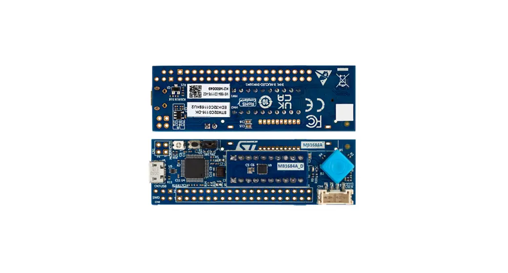
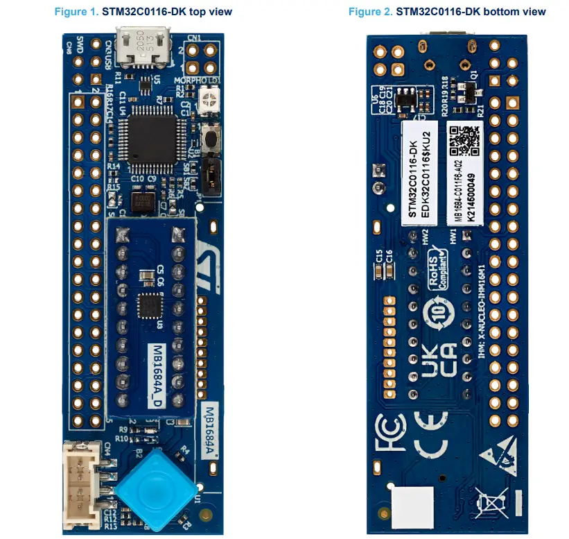
The STM32C0116-DK Discovery kit helps to discover features of the STM32C0 Series microcontroller in a UFQFPN20 package.
This Discovery kit features one UFQFPN20 to DIL20 module designed with the STM32C011F6 microcontroller and allows the user to develop and share applications. It includes an on-board ST-LINK/V2-1 to debug and program the embedded STM32 microcontroller.The STM32C0116-DK Discovery kit is operated by plugging it into a PC through a standard USB Type-A or USB Type-C® Micro-B cable.
Features
- STM32C011F6 Arm® Cortex® ‑M0+ core-based microcontroller with 32 Kbytes of flash memory and 6 Kbytes of RAM, in a UFQFPN20 package
- User LED
- Reset push-button
- 5‑way joystick using a single ADC input pin
- Individual STM32 UFQFPN20 to DIL20 module
Board connectors:
– USB Micro-B
– DIL20 socket
– Dedicated LCD footprint
– Grove (UART)
– 2 x 10‑pin headers for MCU daughterboard
– Extension connectors - On-board ST-LINK/V2-1 debugger/programmer with USB re-enumeration capability: mass storage and debug port
- Comprehensive free software libraries and examples available with the STM32Cube MCU Package
- Support of a wide choice of Integrated Development Environments (IDEs) including IAR Embedded Workbench®, MDK-ARM, and STM32CubeIDE Arm is a registered trademark of Arm Limited (or its subsidiaries) in the US and/or elsewhere.
Ordering information
To order the STM32C0116-DK Discovery kit, refer to Table 1. Additional information is available from the datasheet and reference manual of the target STM32.
Table 1. Ordering information
| Order code | Board reference | Target STM32 |
| STM32C0116-DK | MB1684 | STM32C011F6U6 |
Codification
The meaning of the codification is explained in Table 2.
Table 2. Codification explanation
| STM32C0XXY-DK | Description | Example: STM32C0116-DK |
| STM32C0 | MCU series in STM32 32-bit Arm Cortex MCUs | STM32C0 Series |
| XX | MCU product line in the series | STM32C0x1 product line |
| Y | STM32 flash memory size: • 6 for 32 Kbytes | 32 Kbytes |
| DK | Discovery kit | Discovery kit |
Development environment
3.1 System requirements
- Multi-OS support: Windows° 10, Linux° 64-bit, or macOS°
- USB Type-A or USB Type-C° to Miao-B cable
Note: macOS® is a trademark of Apple Inc.. registered in the U.S. and other countries and regions.
Linux® is a registered trademark of Linus Torvalds.
Al! other trademarks are the property of their respective owners.
3.2 Development toolchains
- IAR Systems® – IAR Embedded Workbench
- Keil® – MDK-ARM
- STMicroelectronics – STM32CubeIDE
On Windows only
3.3 Demonstration software
The demonstration software, included in the STM32Cube MCU Package corresponding to the on-board controller, is preloaded in the STM32 flash memory for easy demonstration of the device peripherals in standalone mode. The latest versions of the demonstration source code and associated documentation can be downloaded from www.st.com.
Conventions
Table 3 provides the conventions used for the ON and OFF settings in the present document.
Table 3. ON/OFF convention
| Convention | Definition |
| Jumper JPx ON | Jumper fitted |
| Jumper JPx OFF | Jumper not fitted |
| Jumper JPx [1-2] | Jumper fitted between Pin 1 and Pin 2 |
| Solder bridge SBx ON | SBx connections closed by 0 Ω resistor |
| Solder bridge SBx OFF | SBx connections left open |
| Resistor Rx ON | Resistor soldered |
| Resistor Rx OFF | Resistor not soldered |
| Capacitor Cx ON | Capacitor soldered |
| Capacitor Cx OFF | Capacitor not soldered |
Quick start
Before installing and using the product, accept the Evaluation Product License Agreement from the www.st.com/epla webpage. For more information on the STM32C0116-DK Discovery kit and demonstration software, visit the STM32C0116-DK product webpage.
5.1 Getting started
Follow the sequence below to configure the Discovery kit and launch the demonstration application (Refer to Figure 3 for component location):
- Check the JP1 jumper position on the board (Refer to Table 4).
- For the correct identification of the device interfaces from the host PC and before connecting the board, install the ST-LINK/V2-1 USB driver, available on the www.st.com website.
- To power the board, connect the Discovery kit to a PC with a Type-A to Micro-B USB cable through the CN3 USB connector of the board.
- Then, the LD1 COM red LED lights up, and the LD3 green LED blinks.
- The demonstration software, as well as other software examples for exploring features, are available in STM32C0116-DK product web page.
Table 4. Jumper configuration
| Jumper | Definition | Position (1) | Comment (1) |
| JP1 | IDD | ON | For current measurement |
Hardware layout and configuration
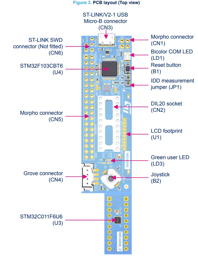
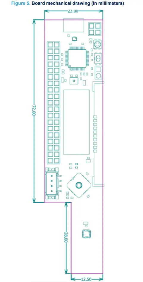
Figure 3 and Figure 4 show the location of the STM32C0116-DK features. The mechanical dimensions of the board are shown in Figure 5.
6.1 PCB layout
Figure 3. PCB layout (Top view)
6.2 Mechanical drawing
6.3 Embedded ST-LINK/V2-1
The embedded ST-LINK/V2-1 supports only the SWD for STM32 devices.
The ST-LINK/V2-1 programming and debugging tool is integrated into the STM32C0116-DK Discovery kit. For information about debugging and programming features, refer to the user manual ST-LINK/V2 in-circuit debugger/programmer for STM8 and STM32 (UM1075), and the technical note Overview of ST-LINK derivatives (TN1235), which describe in detail all the ST-LINK/V2 features.
The additional features supported on the ST-LINK/V2-1 are:
- USB software re-enumeration
- Mass storage interface on USB
- USB power management request for more than 100 mA power on USB Known limitation:
- Activating the readout protection on the STM32 target prevents the target application from running afterward.
The target readout protection must be kept disabled on ST-LINK/V2-1 boards.
6.3.1 Drivers
The ST-LINK/V2-1 requires a dedicated USB driver, which, for Windows 7® and Windows 8® , is found at www.st.com. For Windows 10®, it is not necessary to install the driver, as the ST-LINK is automatically identified.
In case the STM32C0116-DK Discovery kit is connected to the PC before the driver is installed, some Discovery board interfaces may be declared as “Unknown” in the PC device manager. In this case, the user must install the dedicated driver files, and update the driver of the connected device from the device manager as shown in Figure 6.
Note:
Prefer using the “USB Composite Device” handle for a full recovery.
Figure 6. USB composite device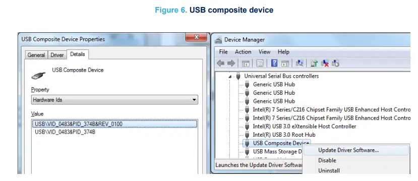
6.3.2 ST-LINK/V2-1 firmware upgrade
The ST-LINK/V2-1 embeds a firmware upgrade mechanism for the in-situ upgrade through the USB port. As the firmware may evolve during the lifetime of the ST-LINK/V2-1 product (for example new functionalities, bug fixes, support for new microcontroller families), it is recommended to visit the www.st.com website before starting to use the STM32C0116-DK Discovery kit and periodically, to stay up-to-date with the latest firmware version.
6.4 Power supply
The STM32C0116-DK Discovery kit is designed to be powered using the CN3 ST-LINK/V2-1 USB connector.
6.5 Board functions
6.5.1 LEDs
LD1 ST-LINK COM LED
The LD1 green and red bicolor LED provides information about the ST-LINK communication status. LD1 default color is red. LD1 turns green to indicate that the communication is in progress between the PC and ST-LINK, with the following setup:
- Blinking red: The first USB enumeration with the PC is taking place
- Red LED ON: When the initialization between the PC andST-LINK is complete
- Blinking red or green: During programming and debugging with target
- Orange ON: Communication failure
LD3 user LED
This green LED is connected to the PB6 GPIO of the STM32C011F6 microcontroller. To light this LED, a LOW logic state must be written in the corresponding GPIO.
6.5.2 Push-buttons
B1 Reset/user button
This push-button is connected to NRST (PF2-NRST) and is used to reset the STM32C0 Series microcontroller or to generate a user event.
B2 joystick
This joystick is a 5‑way rock switch using a single ADC input pin (PA8). Push-in “Select” can be used as a digital user button and EXTI wakeup interrupt. The joystick position for the ADC value refers to Table 5.
Table 5. Joystick position versus ADC value
| Joystick position | Measurement ratio | ADC value (In volts) |
| Select | 0 | 0 |
| Left | 0.2 | 0.67 |
| Down | 0.4 | 1.32 |
| Up | 0.61 | 2.01 |
| Right | 0.8 | 2.65 |
| No key pressed | 1 | 3.3 |
6.5.3 IDD current consumption measurement
The IDD‑labeled JP1 jumper is used to measure the STM32C0 Series microcontroller consumption by removing the jumper and by connecting an ammeter.
- JP1 ON: The STM32C0 Series microcontroller is powered by 3V3 voltage (Default).
- JP1 OFF: An ammeter must be connected to measure the STM32C0 Series microcontroller current. If there is no ammeter, the microcontroller is not powered.
6.5.4 Solder bridges
The solder bridges are located on the top layer of STM32C0116-DK. Their configuration appears in Table 6.
Table 6. Solder bridge configuration
Board connectors
7.1 CN2 DIL20 socket
An STM32 device mounted on a DIL20 module can be programmed or debugged by plugging it into the CN2 socket. The DIL20 socket pinout is detailed in Table 7.
Table 7. DIL20 socket pinout
| Connector | Pin number | Pin name | Port |
| CN2 | 1 | PC15‑OSCX_OUT | Not used |
| 3 | VDD | Power supply | |
| 5 | GND | Ground | |
| 7 | PF2‑NRST | RESET or USER button | |
| 9 | PA0 | Not used | |
| 11 | PA1 | Not used | |
| 13 | PA2 | Grove_USART2_TX | |
| 15 | PA3 | Grove_USART2_RX | |
| 17 | PA4 | LCD_SPI1_NSS | |
| 19 | PA5 | LCD_SPI1_SCK | |
| 2 | PA6 | LCD_SPI1_MISO | |
| 4 | PA7 | LCD_SPI1_MOSI | |
| 6 | PA8 | Joystick with ADC | |
| 8 | PA11 [PA9] | VCP_USART1_TX remap to PA9 | |
| 10 | PA12 [PA10] | VCP_USART1_RX remap to PA10 | |
| 12 | PA13 | Serial wire debug I/O | |
| 14 | PA14‑BOOT0 | Serial wire clock | |
| 16 | PB6 | User LED | |
| 18 | PB7 | Not used | |
| 20 | PC14‑OSCX_IN | Not used |
7.2 CN4 Grove connector
The Grove connector is 4 pins UART connector. It is described in Table 8.
Table 8. Grove connector pinout
| Connector | Pin number | Pin name | Port |
| CN4 | 1 | PA3 | USART2_RX for receiver |
| 2 | PA2 | USART2_TX for transmitter | |
| 3 | VDD | 3.3 V power supply | |
| 4 | GND | Ground |
7.3 CN1/CN5 extension connectors
The silkscreen morpho extension connectors are available on the STM32C0116-DK Discovery kit to support flexibility in user applications. It is described in Table 9.
Table 9. CN1/CN5 extension connectors
| Connector | Pin number | Pin name | Port |
| CN1 | 1 | VDD | – |
| 2 | GPIO | PA2 | |
| 3 | NC | – | |
| 4 | GND | – | |
| CN5 | 1 | NC | – |
| 3 | NC | – | |
| 5 | NC | – | |
| 7 | AVDD | – | |
| 9 | GND | – | |
| 11 | GPIO | PA7 | |
| 13 | GPIO | PA4 | |
| 15 | GPIO | PA8 | |
| 17 | NC | – | |
| 19 | GPIO | PC14 | |
| 21 | GPIO | PA1 | |
| 23 | GPIO | PA0 | |
| 25 | NC | – | |
| 27 | NC | – | |
| 29 | NC | – | |
| 31 | NC | – | |
| 33 | GPIO | PB6 | |
| 35 | NC | – | |
| 37 | NC | – | |
| 2 | GPIO | PC15 | |
| 4 | GPIO | PB7 | |
| 6 | GPIO | PA9 | |
| 8 | 5V | – | |
| 10 | NC | – | |
| 12 | NC | – | |
| 14 | NC | – | |
| 16 | GPIO | PA6 | |
| 18 | GPIO | PA3 | |
| 20 | GND | – | |
| 22 | NC | – | |
| 24 | NC | – | |
| 26 | GPIO | PA5 | |
| 28 | NC | – | |
| 30 | NC | – | |
| 32 | GND | – | |
| 34 | GPIO | PA10 | |
| 36 | NC | – | |
| 38 | NC | – |
STM32C011F6 I/O assignment
The STM32C011F6 pin-out can be directly transposed to the DIL20 module pin-out, as shown in Table 11.
Table 11. STM32C011F6 I/O assignment
| Pin number | Pin name | Description |
| 1 | PC15-OSCX_OUT | Not used |
| 2 | VDD | Power supply |
| 3 | VSS | Ground |
| 4 | PF2-NRST | RESET or USER button |
| 5 | PA0 | Not used |
| 6 | PA1 | Not used |
| 7 | PA2 | Grove_USART2_TX |
| 8 | PA3 | Grove_USART2_RX |
| 9 | PA4 | LCD_SPI1_NSS |
| 10 | PA5 | LCD_SPI1_SCK |
| 11 | PA6 | LCD_SPI1_MISO |
| 12 | PA7 | LCD_SPI1_MOSI |
| 13 | PA8 | Joystick with ADC |
| 14 | PA11 [PA9] | VCP_USART1_TX remap to PA9 |
| 15 | PA12 [PA10] | VCP_USART1_RX remap to PA10 |
| 16 | PA13 | Serial wire debug I/O |
| 17 | PA14-BOOT0 | Serial wire clock |
| 18 | PB6 | User LED |
| 19 | PB7 | Not used |
| 20 | PC14-OSCX_IN | Not used |
STM32C0116-DK board information
9.1 Product marking
The stickers located on the top or bottom side of the PCB provide product information:
- Product order code and product identification for the first sticker
- Board reference with revision, and serial number for the second sticker
On the first sticker, the first line provides the product order code, and the second line the product identification.
On the second sticker, the first line has the following format: “MBxxxx-Variant-yzz”, where “MBxxxx” is the board reference, “Variant” (optional) identifies the mounting variant when several exist, “y” is the PCB revision and “zz” is the assembly revision, for example B01. The second line shows the board serial number used for traceability. Evaluation tools marked as “ES” or “E” are not yet qualified and therefore not ready to be used as reference design or in production. Any consequences deriving from such usage will not be at ST charge. In no event, ST will be liable for any customer usage of these engineering sample tools as reference designs or in production.
“E” or “ES” marking examples of location: - On the targeted STM32 that is soldered on the board (For an illustration of STM32 marking, refer to the STM32 datasheet “Package information” paragraph at the www.st.com website).
- Next to the evaluation tool ordering part number that is stuck or silk-screen printed on the board.
Some boards feature a specific STM32 device version, which allows the operation of any bundled commercial stack/library available. This STM32 device shows a “U” marking option at the end of the standard part number and is not available for sales.
In order to use the same commercial stack in his application, a developer may need to purchase a part number specific to this stack/library. The price of those part numbers includes the stack/library royalties.
9.2 STM32C0116-DK product history
9.2.1 Product identification DK32C0116$KU1
This product identification is based on the MB1684 revision B-01 board.
It embeds the STM32C011F6U6 microcontroller with revision code “A”. The limitations of this revision are detailed in the errata sheet STM32C011 device errata (ES0569).
Product limitations
No limitation identified for this product identification.
9.3 Board revision history
9.3.1 Board MB1684 revision B-01
The revision B-01 is the initial release of the MB1684 board.
Board limitation
No limitation identified for this board revision.
Federal Communications Commission (FCC) and Innovation, Science and Economic Development Canada (ISED) Compliance Statements
10.1 FCC Compliance Statement
Part 15.19
This device complies with Part 15 of the FCC Rules. Operation is subject to the following two conditions: (1) this device may not cause harmful interference, and (2) this device must accept any interference received, including interference that may cause undesired operation.
Part 15.21
Any changes or modifications to this equipment not expressly approved by STMicroelectronics may cause harmful interference and void the user’s authority to operate this equipment.
Part 15.105
This equipment has been tested and found to comply with the limits for a Class B digital device, pursuant to part 15 of the FCC Rules. These limits are designed to provide reasonable protection against harmful interference in a residential installation. This equipment generates uses and can radiate radio frequency energy and, if not installed and used in accordance with the instruction, may cause harmful interference to radio communications.
However, there is no guarantee that interference will not occur in a particular installation. If this equipment does cause harmful interference to radio or television reception which can be determined by turning the equipment off and on, the user is encouraged to try to correct interference by one or more of the following measures:
- Reorient or relocate the receiving antenna.
- Increase the separation between the equipment and receiver.
- Connect the equipment into an outlet on circuit different from that to which the receiver is connected.
- Consult the dealer or an experienced radio/TV technician for help.
Note:
Use only shielded cables.
Responsible party (in the USA)
Terry Blanchard
Americas Region Legal | Group Vice President and Regional Legal Counsel, The Americas
STMicroelectronics, Inc.
750 Canyon Drive | Suite 300 | Coppell, Texas 75019
USA
Telephone: +1 972-466-7845
10.2 ISED Compliance Statement
This device complies with FCC and ISED Canada RF radiation exposure limits set forth for general population for mobile application (uncontrolled exposure). This device must not be collocated or operating in conjunction with any other antenna or transmitter.
Compliance Statement
Notice: This device complies with ISED Canada licence-exempt RSS standard(s). Operation is subject to the following two conditions: (1) this device may not cause interference, and (2) this device must accept any interference, including interference that may cause undesired operation of the device.
ISED Canada ICES-003 Compliance Label: CAN ICES-3 (B) / NMB-3 (B).


