 ALINX ZYNQ FPGA Development Board AC7Z020
 Version Record
| Version | Date | Release By | Description |
| Rev 1.0 | 2020-06-28 | Rachel Zhou | First Release |
AC7Z020 Core Board Introduction
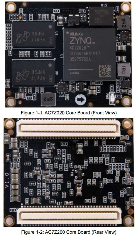
AC7Z020 (core board model, the same below) FPGA core board, ZYNQ chip is based on XC7Z020-2CLG400I of XILINX company ZYNQ7000 series. The ZYNQ chip’s PS system integrates two ARM CortexTM-A9 processors, AMBA® interconnects, internal memory, external memory interfaces and peripherals. The FPGA of the ZYNQ chip contains a wealth of programmable logic cells, DSP and internal RAM.
This core board uses two Micron’s MT41K256M16TW-107 DDR3 chips, each of which has a capacity of 512MB; the two DDR chips combine to form a 32-bit data bus width, and the clock frequency of read and write data between ZYNQ and DDR3 Up to 533Mhz; this configuration can meet the needs of the system’s high-bandwidth data processing
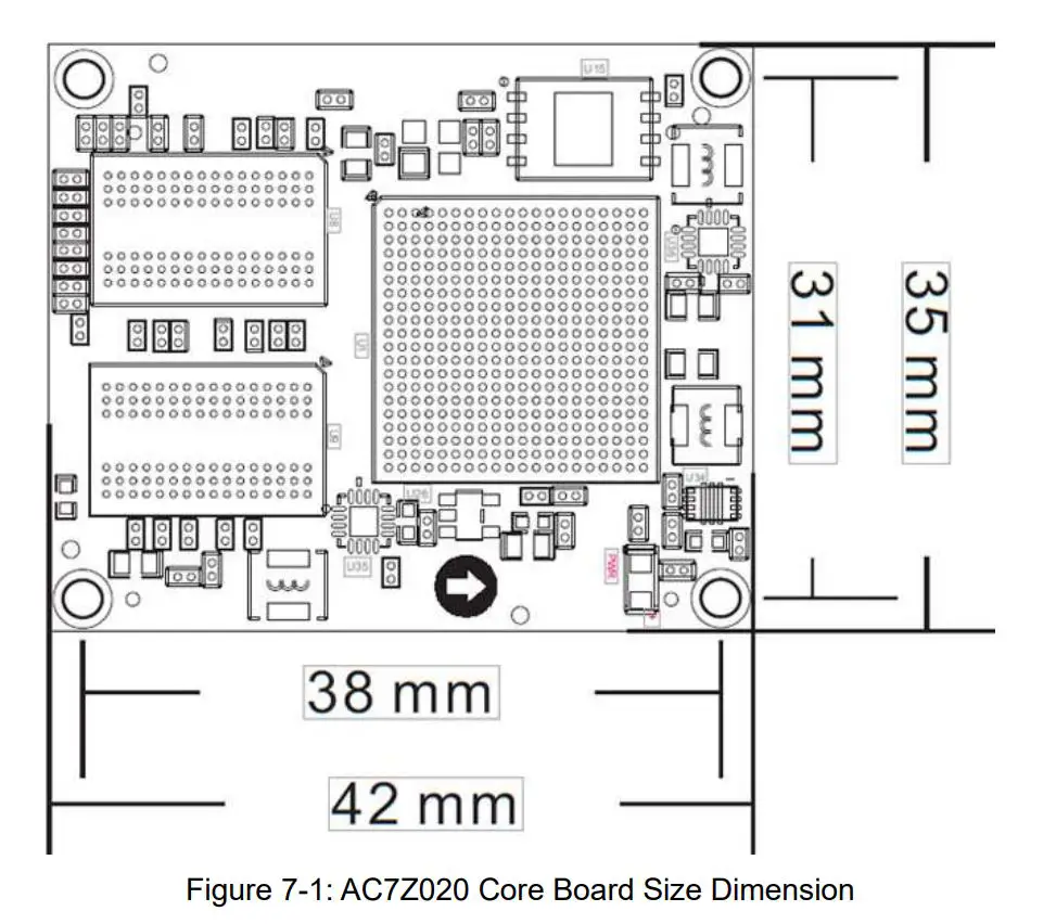
In order to connect with the carrier board, the two board-to-board connectors of this core board are extended with USB ports on the PS side, Gigabit Ethernet interfaces, SD card interfaces, and other remaining MIO ports (48). And almost all IO ports (122) of the BANK13, BAN34 and BANK35 on the PL side, of which the IO levels of BANK34 and BANK35 can be modified by replacing the LDO chip on the core board to meet the user’s requirements for different level interfaces. For users who need a lot of IO, this core board will be a good choice. And the IO connection part, the ZYNQ chip to the interface between the equal length and differential processing, and the core board size is only 35 * 42 (mm), which is very suitable for secondary development.
ZYNQ Chip
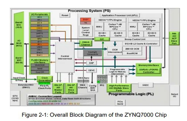
The FPGA core board AC7Z020 uses Xilinx’s Zynq7000 series chip, module XC7Z020-2CLG400I. The chip’s PS system integrates two ARM Cortex™-A9 processors, AMBA® interconnects, internal memory, external memory interfaces and peripherals. These peripherals mainly include USB bus interface, Ethernet-interface, SD/SDIO interface, I2C bus interface, CAN bus interface, UART interface, GPIO etc. The PS can operate independently and start up at power on or reset. Figure 2-1 detailed the Overall Block Diagram of the ZYNQ7000 Chip.
The main parameters of the PS system part are as follows
- ARM dual-core CortexA9-based application processor, ARM-v7 architecture, up to 1GHz
- 32KB level 1 instruction and data cache per CPU, 512KB level 2 cache 2 CPU shares
- On-chip boot ROM and 256KB on-chip RAM
- External storage interface, support 16/32 bit DDR2, DDR3 interface
- Two Gigabit NIC support: divergent-aggregate DMA, GMII, RGMII, SGMII interface
- Two USB2.0 OTG interfaces, each supporting up to 12 nodes
- Two CAN2.0B bus interfaces
- Two SD card, SDIO, MMC compatible controllers
- 2 SPIs, 2 UARTs, 2 I2C interfaces
- 4 pairs of 32bit GPIO, 54 (32 + 22) as PS system IO, 64 connected to PL
- High bandwidth connection within PS and PS to PL
The main parameters of the PL logic part are as follows
- Logic Cells: 85K
- Look-up-tables (LUTs): 53,200
- Flip-flops: 106,400
- 18x25MACCs:220
- Block RAM:4.9Mb
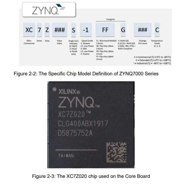
- Two AD converters for on-chip voltage, temperature sensing and up to 17 external differential input channels, 1MBPS XC7Z020-2CLG400I chip speed grade is -2, industrial grade, package is BGA400, pin pitch is 0.8mm the specific chip model definition of ZYNQ7000 series is shown in Figure 2-2
 DDR3 DRAM
 DDR3 DRAM
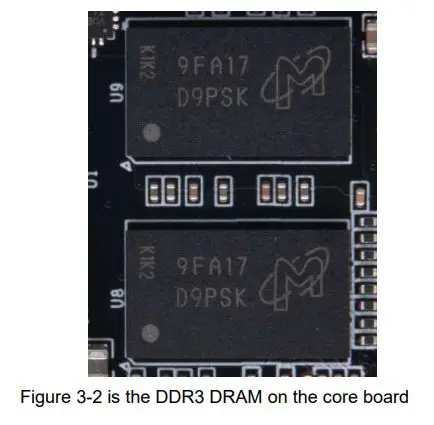
The FPGA core board AC7Z020 is equipped with two Micron 512MB DDR3 SDRAM chips, model MT41K257M16TW-107 (Compatible with Hynix H5TQ4G63AFR-PBI). The total bus width of DDR3 SDRAM is 32bit. DDR3 SDRAM operates at a maximum speed of 533MHz (data rate 1066Mbps). The DDR3 memory system is directly connected to the memory interface of the BANK 502 of the ZYNQ Processing System (PS). The specific configuration of DDR3 SDRAM is shown in Table 3-1 below:
| Bit Number | Chip Model | Capacity | Factory |
| U8,U9 | MT41K256M16TW-107 | 256M x 16bit | Micron |
The hardware design of DDR3 requires strict consideration of signal integrity. We have fully considered the matching resistor/terminal resistance, trace impedance control, and trace length control in circuit design and PCB design to ensure high-speed and stable operation of DDR3. The hardware connection of DDR3 DRAM is shown in Figure 3-1: 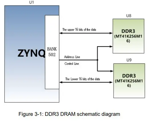
DDR3 DRAM pin assignment
| Signal Name | ZYNQ Pin Name | ZYNQ Pin Number |
| DDR3_DQS0_P | PS_DDR_DQS_P0_502 | C2 |
| DDR3_DQS0_N | PS_DDR_DQS_N0_502 | B2 |
| DDR3_DQS1_P | PS_DDR_DQS_P1_502 | G2 |
| DDR3_DQS1_N | PS_DDR_DQS_N1_502 | F2 |
| DDR3_DQS2_P | PS_DDR_DQS_P2_502 | R2 |
| DDR3_DQS2_N | PS_DDR_DQS_N2_502 | T2 |
| DDR3_DQS3_P | PS_DDR_DQS_P3_502 | W5 |
| DDR3_DQS4_N | PS_DDR_DQS_N3_502 | W4 |
| DDR3_D0 | PS_DDR_DQ0_502 | C3 |
| DDR3_D1 | PS_DDR_DQ1_502 | B3 |
| DDR3_D2 | PS_DDR_DQ2_502 | A2 |
| DDR3_D3 | PS_DDR_DQ3_502 | A4 |
| DDR3_D4 | PS_DDR_DQ4_502 | D3 |
| DDR3_D5 | PS_DDR_DQ5_502 | D1 |
| DDR3_D6 | PS_DDR_DQ6_502 | C1 |
| DDR3_D7 | PS_DDR_DQ7_502 | E1 |
| DDR3_D8 | PS_DDR_DQ8_502 | E2 |
| DDR3_D9 | PS_DDR_DQ9_502 | E3 |
| DDR3_D10 | PS_DDR_DQ10_502 | G3 |
| DDR3_D11 | PS_DDR_DQ11_502 | H3 |
| DDR3_D12 | PS_DDR_DQ12_502 | J3 |
| DDR3_D13 | PS_DDR_DQ13_502 | H2 |
| DDR3_D14 | PS_DDR_DQ14_502 | H1 |
| DDR3_D15 | PS_DDR_DQ15_502 | J1 |
| DDR3_D16 | PS_DDR_DQ16_502 | P1 |
| DDR3_D17 | PS_DDR_DQ17_502 | P3 |
| DDR3_D18 | PS_DDR_DQ18_502 | R3 |
| DDR3_D19 | PS_DDR_DQ19_502 | R1 |
| DDR3_D20 | PS_DDR_DQ20_502 | T4 |
| DDR3_D21 | PS_DDR_DQ21_502 | U4 |
| DDR3_D22 | PS_DDR_DQ22_502 | U2 |
| DDR3_D23 | PS_DDR_DQ23_502 | U3 |
| DDR3_D24 | PS_DDR_DQ24_502 | V1 |
| DDR3_D25 | PS_DDR_DQ25_502 | Y3 |
| DDR3_D26 | PS_DDR_DQ26_502 | W1 |
| DDR3_D27 | PS_DDR_DQ27_502 | Y4 |
| DDR3_D28 | PS_DDR_DQ28_502 | Y2 |
| DDR3_D29 | PS_DDR_DQ29_502 | W3 |
| DDR3_D30 | PS_DDR_DQ30_502 | V2 |
| DDR3_D31 | PS_DDR_DQ31_502 | V3 |
| DDR3_DM0 | PS_DDR_DM0_502 | A1 |
| DDR3_DM1 | PS_DDR_DM1_502 | F1 |
| DDR3_DM2 | PS_DDR_DM2_502 | T1 |
| DDR3_DM3 | PS_DDR_DM3_502 | Y1 |
| DDR3_A0 | PS_DDR_A0_502 | N2 |
| DDR3_A1 | PS_DDR_A1_502 | K2 |
| DDR3_A2 | PS_DDR_A2_502 | M3 |
| DDR3_A3 | PS_DDR_A3_502 | K3 |
| DDR3_A4 | PS_DDR_A4_502 | M4 |
| DDR3_A5 | PS_DDR_A5_502 | L1 |
| DDR3_A6 | PS_DDR_A6_502 | L4 |
| DDR3_A7 | PS_DDR_A7_502 | K4 |
| DDR3_A8 | PS_DDR_A8_502 | K1 |
| DDR3_A9 | PS_DDR_A9_502 | J4 |
| DDR3_A10 | PS_DDR_A10_502 | F5 |
| DDR3_A11 | PS_DDR_A11_502 | G4 |
| DDR3_A12 | PS_DDR_A12_502 | E4 |
| DDR3_A13 | PS_DDR_A13_502 | D4 |
| DDR3_A14 | PS_DDR_A14_502 | F4 |
| DDR3_BA0 | PS_DDR_BA0_502 | L5 |
| DDR3_BA1 | PS_DDR_BA1_502 | R4 |
| DDR3_BA2 | PS_DDR_BA2_502 | J5 |
| DDR3_S0 | PS_DDR_CS_B_502 | N1 |
| DDR3_RAS | PS_DDR_RAS_B_502 | P4 |
| DDR3_CAS | PS_DDR_CAS_B_502 | P5 |
| DDR3_WE | PS_DDR_WE_B_502 | M5 |
| DDR3_ODT | PS_DDR_ODT_502 | N5 |
| DDR3_RESET | PS_DDR_DRST_B_502 | B4 |
| DDR3_CLK0_P | PS_DDR_CKP_502 | L2 |
| DDR3_CLK0_N | PS_DDR_CKN_502 | M2 |
| DDR3_CKE | PS_DDR_CKE_502 | N3 |
QSPI Flash
The FPGA core board AC7Z020 is equipped with one 256MBit Quad-SPI FLASH chip, the flash model is W25Q256FVEI, which uses the 3.3V CMOS voltage standard. Due to the non-volatile nature of QSPI FLASH, it can be used as a boot device for the system to store the boot image of the system. These images mainly include FPGA bit files, ARM application code, and other user data files. The specific models and related parameters of QSPI FLASH are shown in Table 4-1.
| Position | Model | Capacity | Factory |
| U15 | W25Q256FVEI | 32M Byte | Winbond |
QSPI FLASH is connected to the GPIO port of the BANK500 in the PS section of the ZYNQ chip. In the system design, the GPIO port functions of these PS ports need to be configured as the QSPI FLASH interface. Figure 4-1 shows the QSPI Flash in the schematic. 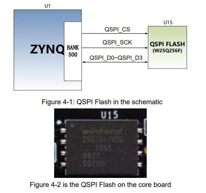
Configure chip pin assignments
| Signal Name | ZYNQ Pin Name | ZYNQ Pin Number |
| QSPI_SCK | PS_MIO6_500 | A5 |
| QSPI_CS | PS_MIO1_500 | A7 |
| QSPI_D0 | PS_MIO2_500 | B8 |
| QSPI_D1 | PS_MIO3_500 | D6 |
| QSPI_D2 | PS_MIO4_500 | B7 |
| QSPI_D3 | PS_MIO5_500 | A6 |
Clock configuration
The AC7Z020 core board provides an active clock for the PS system, so that the PS system can work independently. PS system clock source The ZYNQ chip provides 33.333333MHz clock input for the PS part through the X1 crystal on the core board. The clock input is connected to the PS_CLK_500 pin of the ZYNQ chip BANK500. Its schematic diagram is shown in Figure 2-5-1: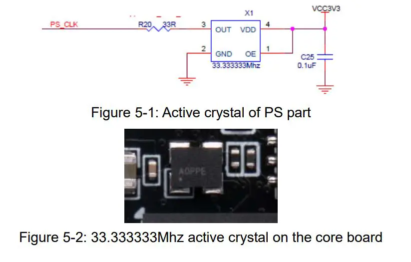
Clock pin assignment
| Signal name | ZYNQ Pin |
| PS_CLK_500 | E7 |
Power Supply
The power supply voltage of the AC7Z020 core board is DC5V, which is supplied by connecting the carrier board. In addition, the power of BANK34 and BANK35 is also provided through the carrier board. The schematic diagram of the power supply design on the core board is shown in Figure 2-6-1: 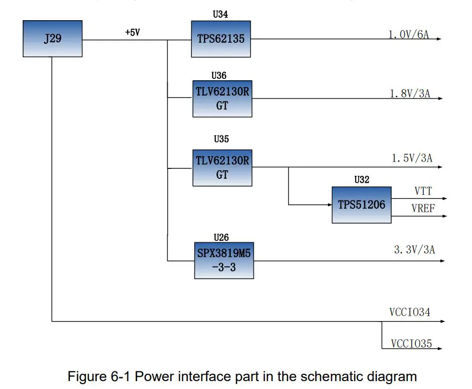
The FPGA development board is powered by + 5V, and is converted into + 1.0V, + 1.8V, + 1.5V, + 3.3V four power supplies through four DC / DC power chips. The output current of + 1.0V can reach 6A, + 1.8V and + 1.5V power output current is 3A, + 3.3V output current is 500mA. J29 also has 4 pins each to supply power to FPGA BANK34 and BANK35. The default is 3.3V. Users can change the power of BANK34 and BANK35 by changing VCCIO34 and VCCIO35 on the backplane. 1.5V generates the VTT and VREF voltages required by DDR3 through TI’s TPS51206. The functions of each power distribution are shown in the following table:
| Power Supply | Function |
| +1.0V | ZYNQ PS and PL section Core Voltage |
| +1.8V | ZYNQ PS and PL partial auxiliary voltage BANK501 IO voltage |
| +3.3V | The VCCIO, QSIP FLASH, Clock Crystal of ZYNQ Bank0, Bank500, Bank13 |
| +1.5V | DDR3, ZYNQ Bank501 |
| VREF,VTT(+0.75V) | DDR3 |
| VCCIO34/35 | Bank34, Bank35 |
Because the power supply of the ZYNQ FPGA has the power-on sequence requirements, in the circuit design, we have designed according to the power requirements of the chip. The power-on sequence is +1.0V->+1.8V->(+1.5 V, +3.3V, VCCIO) circuit design to ensure the normal operation of the chip. Because the level standards of BANK34 and BANK35 are determined by the power supply provided by the carrier board, the highest is 3.3V. When you design the carrier board to provide the VCCIO34 and VCCIO35 power for the core board, the power-on sequence is slower than + 5V.
AC7Z010 Core Board Size Dimension
Board to Board Connectors Pin Assignment
The core board has a total of two high-speed expansion ports. It uses two 120-pin inter-board connectors (J29/J30) to connect to the carrier board. The PIN spacing of the board to board connector is 0.5mm, among them, J29 is connected to 5V power, VCCIO power input, some IO signals and JTAG signals, and J30 is connected to the remaining IO signals and MIO. The IO level of BANK34 and BANK35 can be changed by adjusting the VCCIO inputon the connector, the highest level does not exceed 3.3V. The AX7Z010 carrier board we designed is 3.3V by default. Note that the IO of BANK13 is not available for AC7Z020 core board.
Pin assignment of board to board connector J29
| J29 Pin | Signal Name | ZYNQ Pin | J29 Pin | Signal Name | ZYNQ Pin |
| 1 | VCC5V | – | 2 | VCC5V | – |
| 3 | VCC5V | – | 4 | VCC5V | – |
| 5 | VCC5V | – | 6 | VCC5V | – |
| 7 | VCC5V | – | 8 | VCC5V | – |
| 9 | GND | – | 10 | GND | – |
| 11 | VCCIO_34 | – | 12 | VCCIO_35 | – |
| 13 | VCCIO_34 | – | 14 | VCCIO_35 | – |
| 15 | VCCIO_34 | – | 16 | VCCIO_35 | – |
| 17 | VCCIO_34 | – | 18 | VCCIO_35 | – |
| 19 | GND | – | 20 | GND | – |
| 21 | IO34_L10P | V15 | 22 | IO34_L7P | Y16 |
| 23 | IO34_L10N | W15 | 24 | IO34_L7N | Y17 |
| 25 | IO34_L15N | U20 | 26 | IO34_L17P | Y18 |
| 27 | IO34_L15P | T20 | 28 | IO34_L17N | Y19 |
| 29 | GND | – | 30 | GND | – |
| 31 | IO34_L9N | U17 | 32 | IO34_L8P | W14 |
| 33 | IO34_L9P | T16 | 34 | IO34_L8N | Y14 |
| 35 | IO34_L12N | U19 | 36 | IO34_L3P | U13 |
| 37 | IO34_L12P | U18 | 38 | IO34_L3N | V13 |
| 39 | GND | – | 40 | GND | – |
| 41 | IO34_L14N | P20 | 42 | IO34_L21N | V18 |
| 43 | IO34_L14P | N20 | 44 | IO34_L21P | V17 |
| 45 | IO34_L16N | W20 | 46 | IO34_L18P | V16 |
| 47 | IO34_L16P | V20 | 48 | IO34_L18N | W16 |
| 49 | GND | – | 50 | GND | – |
| 51 | IO34_L22N | W19 | 52 | IO34_L23P | N17 |
| 53 | IO34_L22P | W18 | 54 | IO34_L23N | P18 |
| 55 | IO34_L20N | R18 | 56 | IO34_L13N | P19 |
| 57 | IO34_L20P | T17 | 58 | IO34_L13P | N18 |
| 59 | GND | – | 60 | GND | – |
| 61 | IO34_L19N | R17 | 62 | IO34_L11N | U15 |
| 63 | IO34_L19P | R16 | 64 | IO34_L11P | U14 |
| 65 | IO34_L24P | P15 | 66 | IO34_L5N | T15 |
| 67 | IO34_L24N | P16 | 68 | IO34_L5P | T14 |
| 69 | GND | – | 70 | GND | – |
| 71 | IO34_L4P | V12 | 72 | IO34_L2N | U12 |
| 73 | IO34_L4N | W13 | 74 | IO34_L2P | T12 |
| 75 | IO34_L1P | T11 | 76 | IO34_L6N | R14 |
| 77 | IO34_L1N | T10 | 78 | IO34_L6P | P14 |
| 79 | GND | – | 80 | GND | – |
| 81 | IO13_L13P | Y7 | 82 | IO13_L21P | V11 |
| 83 | IO13_L13N | Y6 | 84 | IO13_L21N | V10 |
| 85 | IO13_L11N | V7 | 86 | IO13_L14N | Y8 |
| 87 | IO13_L11P | U7 | 88 | IO13_L14P | Y9 |
| 89 | GND | – | 90 | GND | – |
| 91 | IO13_L19N | U5 | 92 | IO13_L22N | W6 |
| 93 | IO13_L19P | T5 | 94 | IO13_L22P | V6 |
| 95 | IO13_L16P | W10 | 96 | IO13_L15P | V8 |
| 97 | IO13_L16N | W9 | 98 | IO13_L15N | W8 |
| 99 | GND | – | 100 | GND | – |
| 101 | IO13_L17P | U9 | 102 | IO13_L20P | Y12 |
| 103 | IO13_L17N | U8 | 104 | IO13_L20N | Y13 |
| 105 | IO13_L18P | W11 | 106 | IO13_L12N | U10 |
| 107 | IO13_L18N | Y11 | 108 | IO13_L12P | T9 |
| 109 | GND | – | 110 | GND | – |
| 111 | FPGA_TCK | F9 | 112 | VP | K9 |
| 113 | FPGA_TMS | J6 | 114 | VN | L10 |
| 115 | FPGA_TDO | F6 | 116 | PS_POR_B | C7 |
| 117 | FPGA_TDI | G6 | 118 | FPGA_DONE | R11 |
Pin assignment of board to board connector J30
| J30 Pin | Signal Name | ZYNQ Pin | J30 Pin | Signal Name | ZYNQ Pin |
| 1 | IO35_L1P | C20 | 2 | IO35_L15N | F20 |
| 3 | IO35_L1N | B20 | 4 | IO35_L15P | F19 |
| 5 | IO35_L18N | G20 | 6 | IO35_L5P | E18 |
| 7 | IO35_L18P | G19 | 8 | IO35_L5N | E19 |
| 9 | GND | T13 | 10 | GND | T13 |
| 11 | IO35_L10N | J19 | 12 | IO35_L3N | D18 |
| 13 | IO35_L10P | K19 | 14 | IO35_L3P | E17 |
| 15 | IO35_L2N | A20 | 16 | IO35_L4P | D19 |
| 17 | IO35_L2P | B19 | 18 | IO35_L4N | D20 |
| 19 | GND | T13 | 20 | GND | T13 |
| 21 | IO35_L8P | M17 | 22 | IO35_L9N | L20 |
| 23 | IO35_L8N | M18 | 24 | IO35_L9P | L19 |
| 25 | IO35_L7P | M19 | 26 | IO35_L6P | F16 |
| 27 | IO35_L7N | M20 | 28 | IO35_L6N | F17 |
| 29 | GND | T13 | 30 | GND | T13 |
| 31 | IO35_L17N | H20 | 32 | IO35_L16N | G18 |
| 33 | IO35_L17P | J20 | 34 | IO35_L16P | G17 |
| 35 | IO35_L19N | G15 | 36 | IO35_L13N | H17 |
| 37 | IO35_L19P | H15 | 38 | IO35_L13P | H16 |
| 39 | GND | T13 | 40 | GND | T13 |
| 41 | IO35_L12N | K18 | 42 | IO35_L14N | H18 |
| 43 | IO35_L12P | K17 | 44 | IO35_L14P | J18 |
| 45 | IO35_L24N | J16 | 46 | IO35_L20P | K14 |
| 47 | IO35_L24P | K16 | 48 | IO35_L20N | J14 |
| 49 | GND | T13 | 50 | GND | T13 |
| 51 | IO35_L21N | N16 | 52 | IO35_L11P | L16 |
| 53 | IO35_L21P | N15 | 54 | IO35_L11N | L17 |
| 55 | IO35_L22N | L15 | 56 | IO35_L23P | M14 |
| 57 | IO35_L22P | L14 | 58 | IO35_L23N | M15 |
| 59 | GND | T13 | 60 | GND | T13 |
| 61 | PS_MIO22 | B17 | 62 | PS_MIO50 | B13 |
| 63 | PS_MIO27 | D13 | 64 | PS_MIO45 | B15 |
| 65 | PS_MIO23 | D11 | 66 | PS_MIO46 | D16 |
| 67 | PS_MIO24 | A16 | 68 | PS_MIO41 | C17 |
| 69 | GND | T13 | 70 | GND | T13 |
| 71 | PS_MIO25 | F15 | 72 | PS_MIO7 | D8 |
| 73 | PS_MIO26 | A15 | 74 | PS_MIO12 | D9 |
| 75 | PS_MIO21 | F14 | 76 | PS_MIO10 | E9 |
| 77 | PS_MIO16 | A19 | 78 | PS_MIO11 | C6 |
| 79 | GND | T13 | 80 | GND | T13 |
| 81 | PS_MIO20 | A17 | 82 | PS_MIO9 | B5 |
| 83 | PS_MIO19 | D10 | 84 | PS_MIO14 | C5 |
| 85 | PS_MIO18 | B18 | 86 | PS_MIO8 | D5 |
| 87 | PS_MIO17 | E14 | 88 | PS_MIO0 | E6 |
| 89 | GND | T13 | 90 | GND | T13 |
| 91 | PS_MIO39 | C18 | 92 | PS_MIO13 | E8 |
| 93 | PS_MIO38 | E13 | 94 | PS_MIO47 | B14 |
| 95 | PS_MIO37 | A10 | 96 | PS_MIO48 | B12 |
| 97 | PS_MIO28 | C16 | 98 | PS_MIO49 | C12 |
| 99 | GND | T13 | 100 | GND | T13 |
| 101 | PS_MIO35 | F12 | 102 | PS_MIO52 | C10 |
| 103 | PS_MIO34 | A12 | 104 | PS_MIO51 | B9 |
| 105 | PS_MIO33 | D15 | 106 | PS_MIO40 | D14 |
| 107 | PS_MIO32 | A14 | 108 | PS_MIO44 | F13 |
| 109 | GND | T13 | 110 | GND | T13 |
| 111 | PS_MIO31 | E16 | 112 | PS_MIO15 | C8 |
| 113 | PS_MIO36 | A11 | 114 | PS_MIO42 | E12 |
| 115 | PS_MIO29 | C13 | 116 | PS_MIO43 | A9 |
| 117 | PS_MIO30 | C15 | 118 | PS_MIO53 | C11 |
| 119 | QSPI_D3_PS_MIO5 | A6 | 120 | QSPI_D2_PS_MIO4 | B7 |


