ALINX ZYNQ Ultrascale + FPGA Board AXU2CGA/B  Version Record
 Version Record
| Version | Date | Release By | Description |
| Rev 1.0 | 2021-04-08 | Rachel Zhou | First Release |
Part 1: AXU2CGA/B Introduction
The AXU2CGA/B Board is characterized by its small size and extensive peripherals. The main chip is Xilinx’s Zynq UltraScale+ MPSoCs CG family chip, the model is XCZU2CG-1SFVC784E. The PS side of AXU2CGA is mounted with 2 slices of DDR4 (total 1GB, 32bit) and 1 slice of 256Mb QSPI FLASH. The PS side of AXU2CGB is equipped with 4 DDR4 (total 2GB, 64bit), one 8GB eMMC FLASH memory chip and one 256Mb QSPI FLASH.
Peripheral interfaces include 1 MINI DP interface, 4 USB3.0 interfaces, 1 Gigabit Ethernet interface, 1 USB serial port, 1 PCIE interface, 1 TF card interface, 2 40-pin expansion ports, 2 MIPI Interface, KEYs and LEDs.
The board schematic is as Figure 1-1: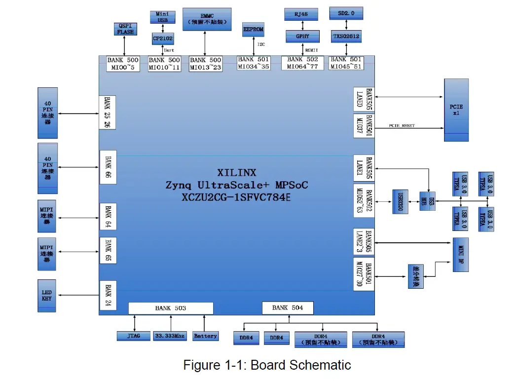
Part 2: ZYNQ Chip
The PS system of the XCZU2CG-1SFVC784E chip integrates two ARM Cortex™-A53 processors with a speed of up to 1.2Ghz and supports Level 2 Cache; it also contains two Cortex-R5 processors with a speed of up to 500Mhz. The XCZU2CG Chip supports 32-bit or 64-bit DDR4, LPDDR4, DDR3, DDR3L, and LPDDR3 memory chips, with rich high-speed interfaces on the PS side such as PCIE Gen2, USB3.0, SATA 3.1, DisplayPort; it also supports USB2.0, Gigabit Ethernet, SD/SDIO, I2C, CAN, UART, GPIO, and other interfaces. The PL end contains a wealth of programmable logic units, DSP and internal RAM. The overall block diagram of the XCZU2CG chip is shown in the Figures 2-1: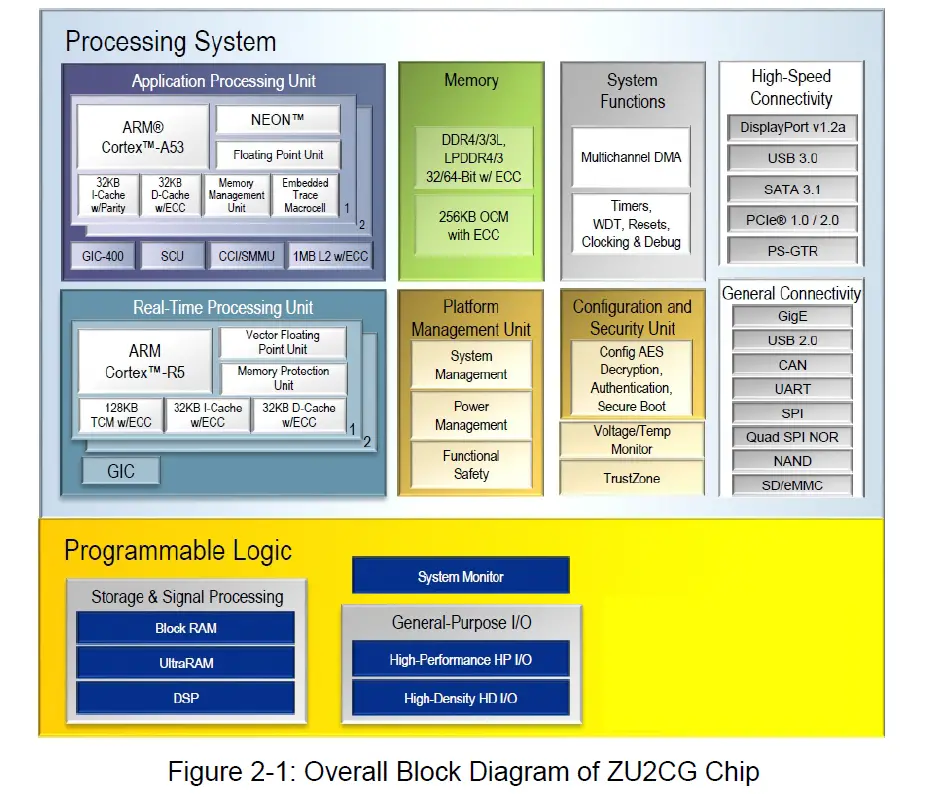
The main parameters of the PS system are as follows:
- ARM dual-core Cortex™-A53 processor, speeds up to 1.2GHz, each CPU 32KB level 1 instruction and data cache, 1MB level 2 cache, shared by 2 CPUs
- ARM dual-core Cortex-R5 processor, speeds up to 500MHz, each CPU 32KB level 1 instruction and data cache, and 128K tightly coupled memory
- External storage interface, support 32/64bit DDR4/3/3L, LPDDR4/3 interface
- Static storage interface, support NAND, 2xQuad-SPI FLASH
- High-speed connection interface, support PCIe Gen2 x4, 2xUSB3.0, SATA 3.1, Display Port, 4 x Tri-mode Gigabit Ethernet
- Common connection interface: 2xUSB2.0, 2x SD/SDIO, 2x UART, 2x CAN 2.0B, 2x I2C, 2x SPI, 4x 32b GPIO
- Power management: support the division of Full/Low/PL/Battery four parts of the power
- Encryption algorithm: support RSA, AES, and SHA
- System monitoring: 10-bit 1Mbps AD sampling for temperature and voltage detection
The main parameters of the PL logic part are as follows:
- Logic Cells: 103K
- flip-flops: 94K
- Lookup table (LUTs) : 47K;
- Block RAM: 5.3Mb
- Clock Management Unit (CMTs) : 3
- Multiplier 18x25MACCs: 240
Part 3: DDR4 DRAM
There are two Micron DDR4 chips on the PS side of the AXU2CGA board, which form a 32-bit data bus bandwidth and a total capacity of 1GB. There are 4 Micron DDR4 chips on the PS side of the AXU2CGB board, which form a 64-bit data bus bandwidth and a total capacity of 2GB. The maximum operating speed of DDR4 SDRAM on the PS side can reach 1200MHz (data rate 2400Mbps). The specific configuration of DDR4 SDRAM is shown below.
Among them, U71 and U72 are only AXU2CGB mounted.
| Location | Capacity | Manufacturer |
| U3,U5,(U71,U72) | 256M x 16bit | Micron |
Table 3-1: DDR4 SDRAM Configuration
The hardware connection of DDR4 on the PS side is shown in Figure 3-1: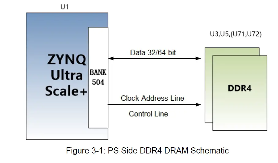
AXU2CGA PS side DDR4 SDRAM Pin Assignment:
| Signal Name | Pin Name | Pin Number |
| PS_DDR4_DQS0_P | PS_DDR_DQS_P0_504 | AF21 |
| PS_DDR4_DQS0_N | PS_DDR_DQS_N0_504 | AG21 |
| PS_DDR4_DQS1_P | PS_DDR_DQS_P1_504 | AF23 |
| PS_DDR4_DQS1_N | PS_DDR_DQS_N1_504 | AG23 |
| PS_DDR4_DQS2_P | PS_DDR_DQS_P2_504 | AF25 |
| PS_DDR4_DQS2_N | PS_DDR_DQS_N2_504 | AF26 |
| PS_DDR4_DQS3_P | PS_DDR_DQS_P3_504 | AE27 |
| PS_DDR4_DQS3_N | PS_DDR_DQS_N3_504 | AF27 |
| PS_DDR4_DQ0 | PS_DDR_DQ0_504 | AD21 |
| PS_DDR4_DQ1 | PS_DDR_DQ1_504 | AE20 |
| PS_DDR4_DQ2 | PS_DDR_DQ2_504 | AD20 |
| PS_DDR4_DQ3 | PS_DDR_DQ3_504 | AF20 |
| PS_DDR4_DQ4 | PS_DDR_DQ4_504 | AH21 |
| PS_DDR4_DQ5 | PS_DDR_DQ5_504 | AH20 |
| PS_DDR4_DQ6 | PS_DDR_DQ6_504 | AH19 |
| PS_DDR4_DQ7 | PS_DDR_DQ7_504 | AG19 |
| PS_DDR4_DQ8 | PS_DDR_DQ8_504 | AF22 |
| PS_DDR4_DQ9 | PS_DDR_DQ9_504 | AH22 |
| PS_DDR4_DQ10 | PS_DDR_DQ10_504 | AE22 |
| PS_DDR4_DQ11 | PS_DDR_DQ11_504 | AD22 |
| PS_DDR4_DQ12 | PS_DDR_DQ12_504 | AH23 |
| PS_DDR4_DQ13 | PS_DDR_DQ13_504 | AH24 |
| PS_DDR4_DQ14 | PS_DDR_DQ14_504 | AE24 |
| PS_DDR4_DQ15 | PS_DDR_DQ15_504 | AG24 |
| PS_DDR4_DQ16 | PS_DDR_DQ16_504 | AC26 |
| PS_DDR4_DQ17 | PS_DDR_DQ17_504 | AD26 |
| PS_DDR4_DQ18 | PS_DDR_DQ18_504 | AD25 |
| PS_DDR4_DQ19 | PS_DDR_DQ19_504 | AD24 |
| PS_DDR4_DQ20 | PS_DDR_DQ20_504 | AG26 |
| PS_DDR4_DQ21 | PS_DDR_DQ21_504 | AH25 |
| PS_DDR4_DQ22 | PS_DDR_DQ22_504 | AH26 |
| PS_DDR4_DQ23 | PS_DDR_DQ23_504 | AG25 |
| PS_DDR4_DQ24 | PS_DDR_DQ24_504 | AH27 |
| PS_DDR4_DQ25 | PS_DDR_DQ25_504 | AH28 |
| PS_DDR4_DQ26 | PS_DDR_DQ26_504 | AF28 |
| PS_DDR4_DQ27 | PS_DDR_DQ27_504 | AG28 |
| PS_DDR4_DQ28 | PS_DDR_DQ28_504 | AC27 |
| PS_DDR4_DQ29 | PS_DDR_DQ29_504 | AD27 |
| PS_DDR4_DQ30 | PS_DDR_DQ30_504 | AD28 |
| PS_DDR4_DQ31 | PS_DDR_DQ31_504 | AC28 |
| PS_DDR4_DM0 | PS_DDR_DM0_504 | AG20 |
| PS_DDR4_DM1 | PS_DDR_DM1_504 | AE23 |
| PS_DDR4_DM2 | PS_DDR_DM2_504 | AE25 |
| PS_DDR4_DM3 | PS_DDR_DM3_504 | AE28 |
| PS_DDR4_A0 | PS_DDR_A0_504 | W28 |
| PS_DDR4_A1 | PS_DDR_A1_504 | Y28 |
| PS_DDR4_A2 | PS_DDR_A2_504 | AB28 |
| PS_DDR4_A3 | PS_DDR_A3_504 | AA28 |
| PS_DDR4_A4 | PS_DDR_A4_504 | Y27 |
| PS_DDR4_A5 | PS_DDR_A5_504 | AA27 |
| PS_DDR4_A6 | PS_DDR_A6_504 | Y22 |
| PS_DDR4_A7 | PS_DDR_A7_504 | AA23 |
| PS_DDR4_A8 | PS_DDR_A8_504 | AA22 |
| PS_DDR4_A9 | PS_DDR_A9_504 | AB23 |
| PS_DDR4_A10 | PS_DDR_A10_504 | AA25 |
| PS_DDR4_A11 | PS_DDR_A11_504 | AA26 |
| PS_DDR4_A12 | PS_DDR_A12_504 | AB25 |
| PS_DDR4_A13 | PS_DDR_A13_504 | AB26 |
| PS_DDR4_WE_B | PS_DDR_A14_504 | AB24 |
| PS_DDR4_CAS_B | PS_DDR_A15_504 | AC24 |
| PS_DDR4_RAS_B | PS_DDR_A16_504 | AC23 |
| PS_DDR4_ACT_B | PS_DDR_ACT_N_504 | Y23 |
| PS_DDR4_ALERT_B | PS_DDR_ALERT_N_504 | U25 |
| PS_DDR4_BA0 | PS_DDR_BA0_504 | V23 |
| PS_DDR4_BA1 | PS_DDR_BA1_504 | W22 |
| PS_DDR4_BG0 | PS_DDR_BG0_504 | W24 |
| PS_DDR4_CS0_B | PS_DDR_CS_N0_504 | W27 |
| PS_DDR4_ODT0 | PS_DDR_ODT0_504 | U28 |
| PS_DDR4_PARITY | PS_DDR_PARITY_504 | V24 |
| PS_DDR4_RESET_B | PS_DDR_RST_N_504 | U23 |
| PS_DDR4_CLK0_P | PS_DDR_CK0_P_504 | W25 |
| PS_DDR4_CLK0_N | PS_DDR_CK0_N_504 | W26 |
| PS_DDR4_CKE0 | PS_DDR_CKE0_504 | V28 |
AXU2CGB PS side DDR4 SDRAM data pin assignment is the same as
AXU2CGA, additional data signal assignment is as follows:
| Signal Name | Pin Name | Pin Number |
| PS_DDR4_DQS4_P | PS_DDR_DQS_P4_504 | N23 |
| PS_DDR4_DQS4_N | PS_DDR_DQS_N4_504 | M23 |
| PS_DDR4_DQS5_P | PS_DDR_DQS_P5_504 | L23 |
| PS_DDR4_DQS5_N | PS_DDR_DQS_N5_504 | K23 |
| PS_DDR4_DQS6_P | PS_DDR_DQS_P6_504 | N26 |
| PS_DDR4_DQS6_N | PS_DDR_DQS_N6_504 | N27 |
| PS_DDR4_DQS7_P | PS_DDR_DQS_P7_504 | J26 |
| PS_DDR4_DQS7_N | PS_DDR_DQS_N7_504 | J27 |
| PS_DDR4_DQ32 | PS_DDR_DQ32_504 | T22 |
| PS_DDR4_DQ33 | PS_DDR_DQ33_504 | R22 |
| PS_DDR4_DQ34 | PS_DDR_DQ34_504 | P22 |
| PS_DDR4_DQ35 | PS_DDR_DQ35_504 | N22 |
| PS_DDR4_DQ36 | PS_DDR_DQ36_504 | T23 |
| PS_DDR4_DQ37 | PS_DDR_DQ37_504 | P24 |
| PS_DDR4_DQ38 | PS_DDR_DQ38_504 | R24 |
| PS_DDR4_DQ39 | PS_DDR_DQ39_504 | N24 |
| PS_DDR4_DQ40 | PS_DDR_DQ40_504 | H24 |
| PS_DDR4_DQ41 | PS_DDR_DQ41_504 | J24 |
| PS_DDR4_DQ42 | PS_DDR_DQ42_504 | M24 |
| PS_DDR4_DQ43 | PS_DDR_DQ43_504 | K24 |
| PS_DDR4_DQ44 | PS_DDR_DQ44_504 | J22 |
| PS_DDR4_DQ45 | PS_DDR_DQ45_504 | H22 |
| PS_DDR4_DQ46 | PS_DDR_DQ46_504 | K22 |
| PS_DDR4_DQ47 | PS_DDR_DQ47_504 | L22 |
| PS_DDR4_DQ48 | PS_DDR_DQ48_504 | M25 |
| PS_DDR4_DQ49 | PS_DDR_DQ49_504 | M26 |
| PS_DDR4_DQ50 | PS_DDR_DQ50_504 | L25 |
| PS_DDR4_DQ51 | PS_DDR_DQ51_504 | L26 |
| PS_DDR4_DQ52 | PS_DDR_DQ52_504 | K28 |
| PS_DDR4_DQ53 | PS_DDR_DQ53_504 | L28 |
| PS_DDR4_DQ54 | PS_DDR_DQ54_504 | M28 |
| PS_DDR4_DQ55 | PS_DDR_DQ55_504 | N28 |
| PS_DDR4_DQ56 | PS_DDR_DQ56_504 | J28 |
| PS_DDR4_DQ57 | PS_DDR_DQ57_504 | K27 |
| PS_DDR4_DQ58 | PS_DDR_DQ58_504 | H28 |
| PS_DDR4_DQ59 | PS_DDR_DQ59_504 | H27 |
| PS_DDR4_DQ60 | PS_DDR_DQ60_504 | G26 |
| PS_DDR4_DQ61 | PS_DDR_DQ61_504 | G25 |
| PS_DDR4_DQ62 | PS_DDR_DQ62_504 | K25 |
| PS_DDR4_DQ63 | PS_DDR_DQ63_504 | J25 |
| PS_DDR4_DM4 | PS_DDR_DM4_504 | R23 |
| PS_DDR4_DM5 | PS_DDR_DM5_504 | H23 |
| PS_DDR4_DM6 | PS_DDR_DM6_504 | L27 |
| PS_DDR4_DM7 | PS_DDR_DM7_504 | H26 |
Part 4: QSPI Flash
The AXU2CGA/B board has a 256MBit Quad-SPI FLASH chip, the model is MT25QU256ABA1EW9-0SIT. QSPI FLASH is connected to the GPIO port of BANK500 in the PS part of the ZYNQ chip. Figure 4-1 shows the part of QSPI Flash in the schematic.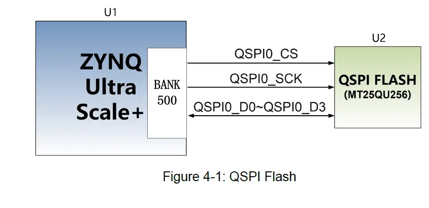
Configure Chip Pin Assignment:
| Signal Name | Pin Name | Pin Number |
| MIO0_QSPI0_SCLK | PS_MIO0_500 | AG15 |
| MIO1_QSPI0_IO1 | PS_MIO1_500 | AG16 |
| MIO2_QSPI0_IO2 | PS_MIO2_500 | AF15 |
| MIO3_QSPI0_IO3 | PS_MIO3_500 | AH15 |
| MIO4_QSPI0_IO0 | PS_MIO4_500 | AH16 |
| MIO5_QSPI0_SS_B | PS_MIO5_500 | AD16 |
Part 5: eMMC Flash (Only for AXU2CGB)
There is an eMMC FLASH chip with a capacity of 8GB on the AXU2CGB board. The eMMC FLASH is connected to the GPIO port of the BANK500 of the PS part of ZYNQ UltraScale+. Figure 5-1 is the eMMC Flash schematic.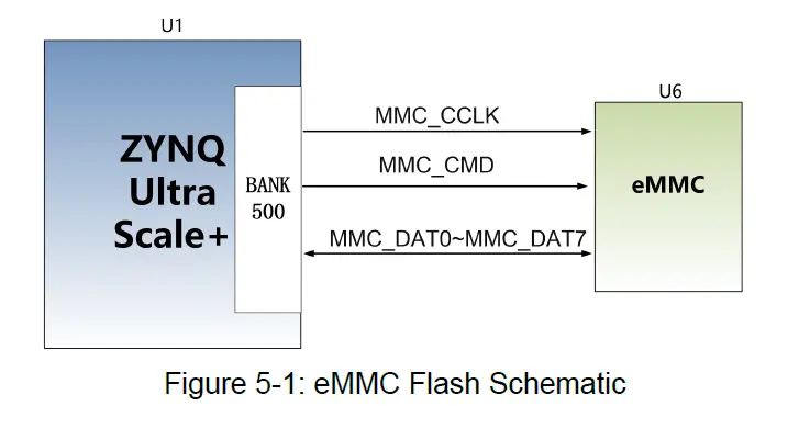
Configure Chip Pin Assignment:
| Signal Name | Pin Name | Pin Number |
| MMC_DAT0 | PS_MIO13_500 | AH18 |
| MMC_DAT1 | PS_MIO14_500 | AG18 |
| MMC_DAT2 | PS_MIO15_500 | AE18 |
| MMC_DAT3 | PS_MIO16_500 | AF18 |
| MMC_DAT4 | PS_MIO17_500 | AC18 |
| MMC_DAT5 | PS_MIO18_500 | AC19 |
| MMC_DAT6 | PS_MIO19_500 | AE19 |
| MMC_DAT7 | PS_MIO20_500 | AD19 |
| MMC_CMD | PS_MIO21_500 | AC21 |
| MMC_CCLK | PS_MIO22_500 | AB20 |
| MMC_RSTN | PS_MIO23_500 | AB18 |
Part 6: EEPROM
The AXU2CGA/B development board has a piece of EEPROM onboard, the model number is 24LC04. The I2C signal of the EEPROM is connected to the MIO port of the ZYNQ PS side. Figure 6-1 is EEPROM schematic: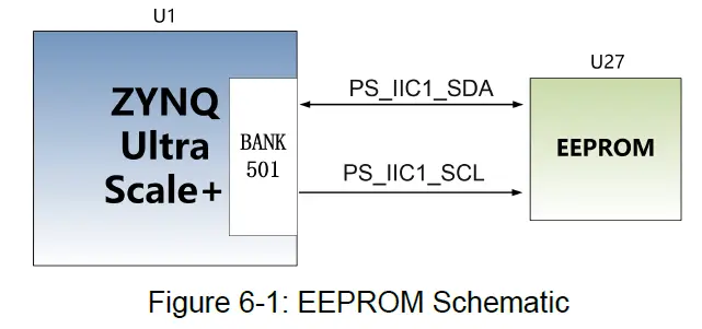
EEPROM Pin Assignment:
| Signal Name | Pin Name | Pin Number |
| PS_IIC1_SCL | PS_MIO32_501 | J16 |
| PS_IIC1_SDA | PS_MIO33_501 | L16 |
Part 7: DP Display Interface
The AXU2CGA/B board has a MINI-type DisplayPort output display interface, which is used for video image display, and supports up to 4K x 2K@30Fps output. The TX signals of LANE0 and LANE1 of ZU2CG PS MGT are connected to the DP connector in a differential signal mode. The DisplayPort auxiliary channel is connected to the MIO pin of the PS. The schematic diagram of the DP output interface is shown in Figure 7-1: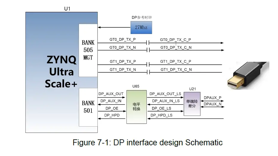
The DisplayPort interface ZYNQ pin assignment is as follows:
| Signal Name | ZYNQ Pin Number | ZYNQ Pin Number | Description |
| GT0_DP_TX_P | PS_MGTTXP3_505 | B23 | Low bits of DP Data Transmit Positive |
| GT0_DP_TX_N | PS_MGTTXN3_505 | B24 | Low bits of DP Data Transmit Negative |
| GT1_DP_TX_P | PS_MGTTXP2_505 | C25 | High bits of DP Data Transmit Positive |
| GT1_DP_TX_N | PS_MGTTXN2_505 | C26 | High bits of DP Data Transmit Negative |
| 505_DP_CLKP | PS_MGTREFCLK2P_50 5 | C21 | DP Reference Clock Positive |
| 505_DP_CLKP | PS_MGTREFCLK2N_50 5 | C22 | DP Reference Clock Negative |
| DP_AUX_OUT | PS_MIO27 | J15 | DP Auxiliary Data Output |
| DP_AUX_IN | PS_MIO30 | F16 | DP Auxiliary Data Input |
| DP_OE | PS_MIO29 | G16 | DP Auxiliary Data Output Enable |
| DP_HPD | PS_MIO28 | K15 | DP Insertion Signal Detection |
Part 8: USB 3.0 Interface
There are 4 USB3.0 interfaces on the AXU2CGA/B board, the interface is HOST working mode (Type A), and the data transmission speed is up to 5.0Gb/s. The USB3.0 interfaces connect external USB PHY chip and USB3.0 HUB chip through ULPI interface to realize high-speed USB3.0 data communication.
The USB Schematic is shown in Figure 8-1: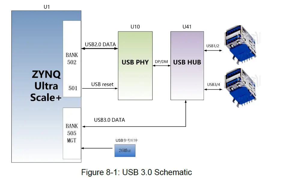
USB Pin Assignment:
| Signal Name | Pin Name | Pin Number | Description |
| USB_SSTXP | PS_MGTTXP2_505 | D23 | USB3.0 Data Transmission Positive |
| USB_SSTXN | PS_MGTTXN2_505 | D24 | USB3.0 Data Transmission Negative |
| USB_SSRXP | PS_MGTRXP2_505 | D27 | USB3.0 Data Receive Positive |
| USB_SSRXN | PS_MGTRXN2_505 | D28 | USB3.0 Data Receive Negative |
| 505_USB_CLKP | PS_MGTREFCLK2P_505 | E21 | USB3.0 Reference Clock Positive |
| 505_USB_CLKN | PS_MGTREFCLK2N_505 | E22 | USB3.0 Reference Clock Negative |
| USB_DATA0 | PS_MIO56 | C16 | USB2.0 Data Bit0 |
| USB_DATA1 | PS_MIO57 | A16 | USB2.0 Data Bit1 |
| USB_DATA2 | PS_MIO54 | F17 | USB2.0 Data Bit2 |
| USB_DATA3 | PS_MIO59 | E17 | USB2.0 Data Bit3 |
| USB_DATA4 | PS_MIO60 | C17 | USB2.0 Data Bit4 |
| USB_DATA5 | PS_MIO61 | D17 | USB2.0 Data Bit5 |
| USB_DATA6 | PS_MIO62 | A17 | USB2.0 Data Bit6 |
| USB_DATA7 | PS_MIO63 | E18 | USB2.0 Data Bit7 |
| USB_STP | PS_MIO58 | F18 | USB2.0 Stop Signal |
| USB_DIR | PS_MIO53 | D16 | USB2.0 Data Direction Signal |
| USB_CLK | PS_MIO52 | G18 | USB2.0 Clock Signal |
| USB_NXT | PS_MIO55 | B16 | USB2.0 the NEXT Data Signal |
Part 9: Gigabit Ethernet Interface
There is 1 Gigabit Ethernet interface on AXU2CGA/B, and the Ethernet interface is on BANK502 of PS connected through the GPHY chip. The GPHY chip uses the KSZ9031RNXIC Ethernet PHY chip from Micrel, and the PHY Address is 001. Figure 9-1 is a schematic diagram of the connection of the Ethernet PHY chip on the ZYNQ PS side: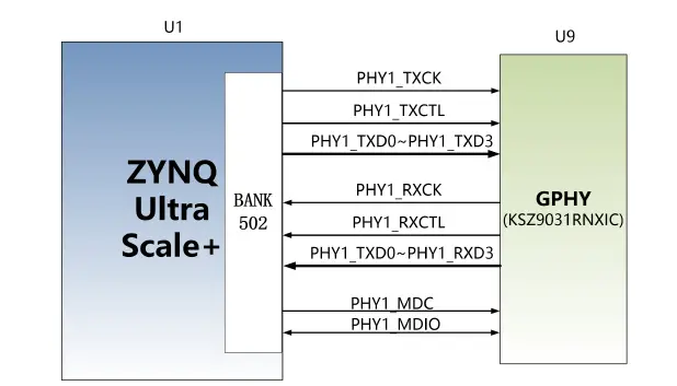
The Gigabit Ethernet pin assignments are as follows:
| Signal Name | Pin Name | Pin Number | Description |
| PHY1_TXCK | PS_MIO64 | E19 | RGMII Transmit Clock |
| PHY1_TXD0 | PS_MIO65 | A18 | Transmit data bit0 |
| PHY1_TXD1 | PS_MIO66 | G19 | Transmit data bit1 |
| PHY1_TXD2 | PS_MIO67 | B18 | Transmit data bit2 |
| PHY1_TXD3 | PS_MIO68 | C18 | Transmit data bit3 |
| PHY1_TXCTL | PS_MIO69 | D19 | Transmit data Enable Signal |
| PHY1_RXCK | PS_MIO70 | C19 | RGMII Receive Clock |
| PHY1_RXD0 | PS_MIO71 | B19 | Receive Data Bit0 |
| PHY1_RXD1 | PS_MIO72 | G20 | Receive Data Bit1 |
| PHY1_RXD2 | PS_MIO73 | G21 | Receive Data Bit2 |
| PHY1_RXD3 | PS_MIO74 | D20 | Receive Data Bit3 |
| PHY1_RXCTL | PS_MIO75 | A19 | Receive Data Enable Signal |
| PHY1_MDC | PS_MIO76 | B20 | MDIO Clock Management |
| PHY1_MDIO | PS_MIO77 | F20 | MDIO Management Data |
Part 10: USB to Serial Port
There is a Uart to USB interface on the AXU2CGA/B board for system debugging. The conversion chip uses the USB-UAR chip of Silicon Labs CP2102, and the USB interface uses the MINI USB interface. It can be connected to the USB port of the PC with a USB cable for independent power supply of the core board and serial data communication. The schematic diagram of the USB Uart circuit design is shown in Figure 10-1: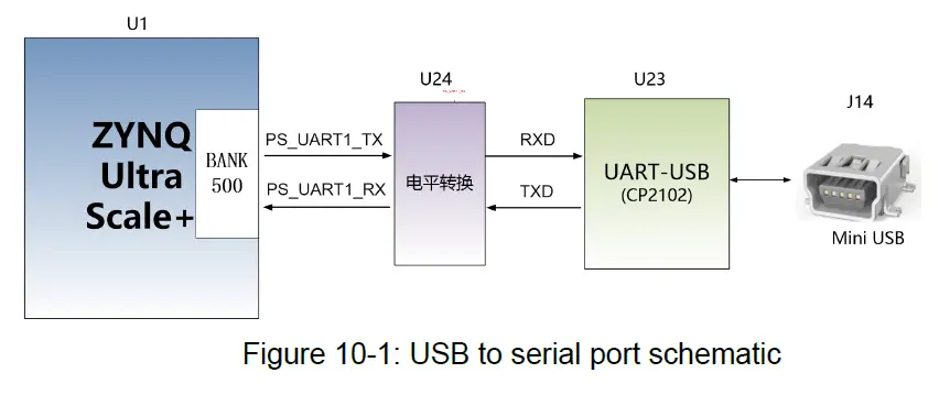
USB to serial port ZYNQ pin assignment:
| Signal name | Pin Name | Pin Number | Description |
| PS_UART1_TX | PS_MIO24 | AB19 | PL Uart Data Output |
| PS_UART1_RX | PS_MIO25 | AB21 | PL Uart Data Input |
Part 11: SD Card Slot Interface
The AXU2CGA/B board contains a Micro SD card interface. The SDIO signal is connected to the IO signal of BANK501. The SD card connector schematic is shown in Figure 11-1.
SD card slot pin assignment:
| Signal Name | Pin Name | Pin Number | Description |
| SD_CLK | PS_MIO51 | l21 | SD Clock Signal |
| SD_CMD | PS_MIO50 | M19 | SD Command Signal |
| SD_D0 | PS_MIO46 | L20 | SD Data0 |
| SD_D1 | PS_MIO47 | H21 | SD Data1 |
| SD_D2 | PS_MIO48 | J21 | SD Data2 |
| SD_D3 | PS_MIO49 | M18 | SD Data3 |
| SD_CD | PS_MIO45 | K20 | SD Card Detection Signal |
Part 12: PCIE Interface
There is a PCIE x1 slot on the AXU2CGA/B board for connecting PCIE peripherals, and the PCIE communication speed is up to 5Gbps. PCIE signal is directly connected to LANE0 of BANK505 PS MGT transceiver. The schematic diagram of PCIE x 1 design is shown in Figure 12-1: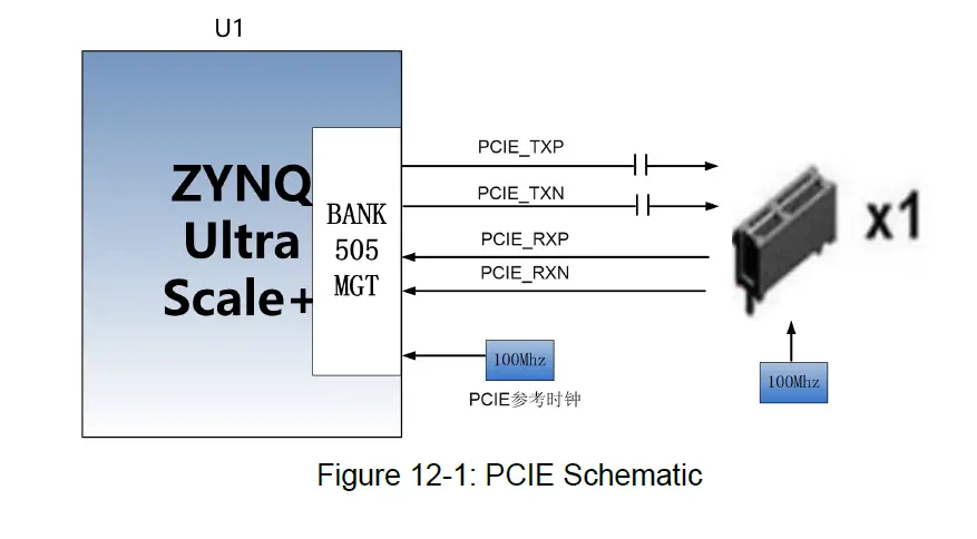
PCIE Interface ZYNQ Pin Assignment
| Signal Name | Pin Name | Pin Number | Description |
| PCIE_TXP | PS_MGTTXP0_505 | E25 | PCIE Data Transmission Positive |
| PCIE_TXN | PS_MGTTXN0_505 | E26 | PCIE Data Transmission Negative |
| PCIE_RXP | PS_MGTRXP0_505 | F27 | PCIE Data Receive Positive |
| PCIE_RXN | PS_MGTRXN0_505 | F28 | PCIE Data Receive Negative |
| PCIE_REFCLK_P | PS_MGTREFCLK0P_505 | F23 | PCIE Data Reference Clock Positive |
| PCIE_REFCLK_N | PS_MGTREFCLK0N_505 | F24 | PCIE Data Reference Clock Negative |
Part 13: 40-Pin Expansion Header
The AXU2CGA/B board is reserved with two 0.1-inch standard pitch 40-pin expansion ports J12 and J15, which are used to connect the ALINX modules or the external circuit designed by the user. The expansion port has 40 signals, of which 1-channel 5V power supply, 2-channel 3.3 V power supply, 3-channel ground, and 34 IOs. Do not directly connect the IO directly to the 5V device to avoid burning the FPGA. If you want to connect 5V equipment, you need to connect the level conversion chip.
The IO port of the J15 expansion port is connected to the ZYNQ chip BANK25 and BANK26, and the level standard is 3.3V. The schematic diagram of the design is shown in Figure 13-1: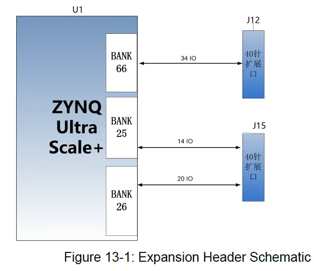
J12 Expansion Header ZYNQ Pin Assignment
| J12 Pin | Signal Name | Pin Number | J12 Pin | Signal Name | Pin Number |
| 1 | GND | – | 2 | VCC5V | – |
| 3 | IO1_1N | F7 | 4 | IO1_1P | G8 |
| 5 | IO1_2N | F6 | 6 | IO1_2P | G6 |
| 7 | IO1_3N | D9 | 8 | IO1_3P | E9 |
| 9 | IO1_4N | F5 | 10 | IO1_4P | G5 |
| 11 | IO1_5N | E8 | 12 | IO1_5P | F8 |
| 13 | IO1_6N | D5 | 14 | IO1_6P | E5 |
| 15 | IO1_7N | C4 | 16 | IO1_7P | D4 |
| 17 | IO1_8N | E3 | 18 | IO1_8P | E4 |
| 19 | IO1_9N | F1 | 20 | IO1_9P | G1 |
| 21 | IO1_10N | E2 | 22 | IO1_10P | F2 |
| 23 | IO1_11N | D6 | 24 | IO1_11P | D7 |
| 25 | IO1_12N | B9 | 26 | IO1_12P | C9 |
| 27 | IO1_13N | A4 | 28 | IO1_13P | B4 |
| 29 | IO1_14N | B6 | 30 | IO1_14P | C6 |
| 31 | IO1_15N | A6 | 32 | IO1_15P | A7 |
| 33 | IO1_16N | B8 | 34 | IO1_16P | C8 |
| 35 | IO1_17N | A8 | 36 | IO1_17P | A9 |
| 37 | GND | – | 38 | GND | – |
| 39 | VCC_3V3_BUCK4 | – | 40 | VCC_3V3_BUCK4 | – |
J15 Expansion Header ZYNQ Pin Assignment
| J15 Pin | Signal Name | Pin Number | J15 Pin | Signal Name | Pin Number |
| 1 | GND | – | 2 | VCC5V | – |
| 3 | IO2_1N | A11 | 4 | IO2_1P | A12 |
| 5 | IO2_2N | A13 | 6 | IO2_2P | B13 |
| 7 | IO2_3N | A14 | 8 | IO2_3P | B14 |
| 9 | IO2_4N | E13 | 10 | IO2_4P | E14 |
| 11 | IO2_5N | A15 | 12 | IO2_5P | B15 |
| 13 | IO2_6N | C13 | 14 | IO2_6P | C14 |
| 15 | IO2_7N | B10 | 16 | IO2_7P | C11 |
| 17 | IO2_8N | D14 | 18 | IO2_8P | D15 |
| 19 | IO2_9N | F11 | 20 | IO2_9P | F12 |
| 21 | IO2_10N | H13 | 22 | IO2_10P | H14 |
| 23 | IO2_11N | G14 | 24 | IO2_11P | G15 |
| 25 | IO2_12N | F10 | 26 | IO2_12P | G11 |
| 27 | IO2_13N | H12 | 28 | IO2_13P | J12 |
| 29 | IO2_14N | J14 | 30 | IO2_14P | K14 |
| 31 | IO2_15N | K12 | 32 | IO2_15P | K13 |
| 33 | IO2_16N | L13 | 34 | IO2_16P | L14 |
| 35 | IO2_17N | G10 | 36 | IO2_17P | H11 |
| 37 | GND | – | 38 | GND | – |
| 39 | VCC_3V3_BUCK4 | – | 40 | VCC_3V3_BUCK4 | – |
Part 14: MIPI Camera Interface
There are 2 MIPI interfaces on the AXU2CGA/B board for connecting MIPI cameras. The differential signal of MIPI is connected to the HP IO of BANK64 and 65, and the level standard is +1.2V; the control signal of MIPI is connected to BANK24, and the level standard is +3.3V. The schematic diagram of the MIPI port design is shown in Figure 14-1: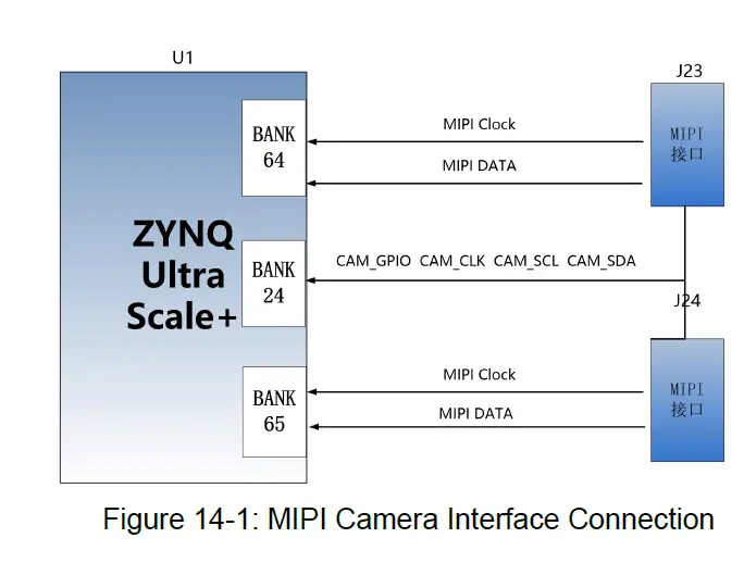
MIPI Interface J23 Pin Assignment
| PIN | Signal Name | ZYNQ Pin Name | ZYNQ Pin Number | Description |
| 1 | GND | – | – | Ground |
| 2 | MIPI1_LAN0_N | IO_L2N_64 | AE8 | MIPI Data 0 Signal N |
| 3 | MIPI1_LAN0_P | IO_L2P_64 | AE9 | MIPI Data 0 Signal P |
| 4 | GND | – | – | Ground |
| 5 | MIPI1_LAN1_N | IO_L3N_64 | AC8 | MIPI Data 1 Signal N |
| 6 | MIPI1_LAN1_P | IO_L3P_64 | AB8 | MIPI Data 1 Signal P |
| 7 | GND | – | – | Ground |
| 8 | MIPI1_CLK_N | IO_L1N_64 | AD9 | MIPI Clock Signal N |
| 9 | MIPI1_CLK_P | IO_L1P_64 | AC9 | MIPI Clock Signal P |
| 10 | GND | – | – | Ground |
| 11 | CAM1_GPIO | IO_L2N_24 | AH14 | Control Signal IO |
| 12 | CAM1_CLK | IO_L3P_24 | AG13 | Control Signal Clock |
| 13 | CAM1_SCL | IO_L3N_24 | AH13 | Control Signal SCL |
| 14 | CAM1_SDA | IO_L4P_24 | AE13 | Control Signal SDA |
| 15 | VCC_3V3 | – | – | 3.3V Power Supply |
MIPI Interface J24 Pin Assignment
| PIN | Signal Name | ZYNQ Pin Name | ZYNQ Pin Number | Description |
| 1 | GND | – | – | Ground |
| 2 | MIPI2_LAN0_N | IO_L2N_65 | V9 | MIPI Data 0 Signal N |
| 3 | MIPI2_LAN0_P | IO_L2P_65 | U9 | MIPI Data 0 Signal P |
| 4 | GND | – | – | Ground |
| 5 | MIPI2_LAN1_N | IO_L3N_65 | V8 | MIPI Data 1 Signal N |
| 6 | MIPI2_LAN1_P | IO_L3P_65 | U8 | MIPI Data 1 Signal P |
| 7 | GND | – | – | Ground |
| 8 | MIPI2_CLK_N | IO_L1N_65 | Y8 | MIPI Clock Signal N |
| 9 | MIPI2_CLK_P | IO_L1P_65 | W8 | MIPI Clock Signal P |
| 10 | GND | – | – | Ground |
| 11 | CAM2_GPIO | IO_L5P_24 | AD15 | Control Signal IO |
| 12 | CAM2_CLK | IO_L6P_24 | AC14 | Control Signal Clock |
| 13 | CAM2_SCL | IO_L5N_24 | AD14 | Control Signal SCL |
| 14 | CAM2_SDA | IO_L6N_24 | AC13 | Control Signal SDA |
| 15 | VCC_3V3 | – | – | 3.3V Power Supply |
Part 15: JTAG Debug Port
The 10-pin JTAG interface is reserved on the AXU2CGA/B board for downloading ZYNQ UltraScale+ programs or firmware programs to FLASH. The pin definition of JTAG is shown in the figure below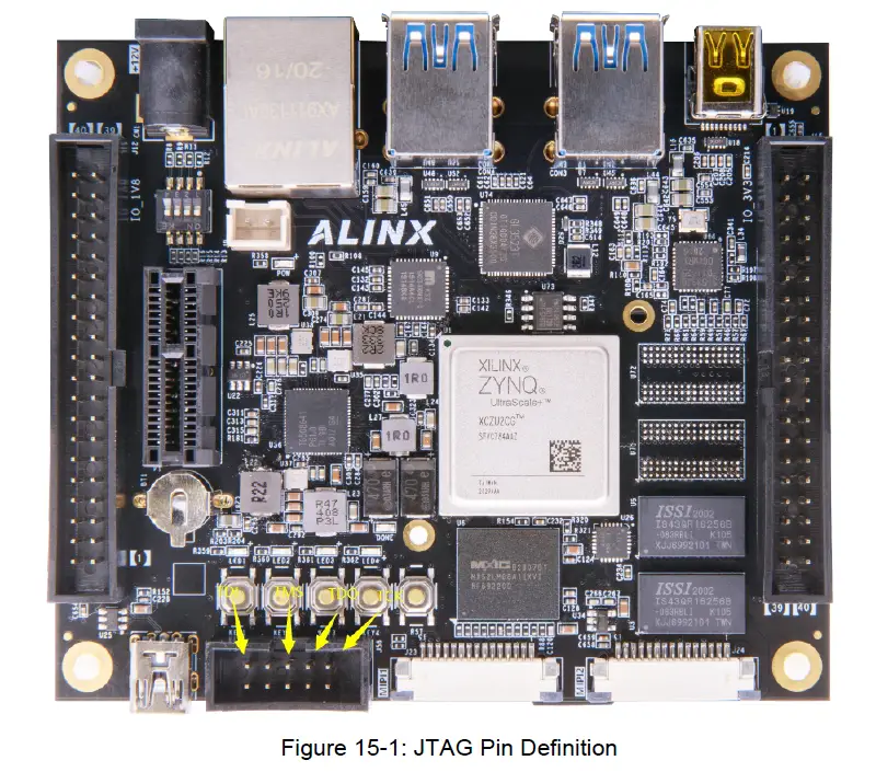
Part 16: DIP Switch Configuration
There is a 4-digit DIP switch SW1 on the FPGA development board to configure the startup mode of the ZYNQ system. The AXU2CGA/B system development platform supports 4 startup modes. The 4 startup modes are JTAG debug mode, QSPI FLASH, EMMC and SD2.0 card startup mode. After the ZU3EG chip is powered on, it will detect the level of (PS_MODE0~3) to determine the startup mode. The user can select different startup modes through the DIP switch SW1 on the expansion board. The SW1 startup mode configuration is shown in the following table 16-1.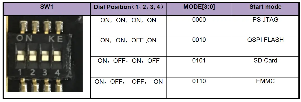
Table 16-1: SW1 startup mode configuration
Part 17: LEDs
There are 4 user indicator lights, 4 user control KEYs, and a reset KET on the AXU2CGA/B board. 4 user indicators and 4 user KEYs are all connected to the IO of BANK24. The schematic diagram of the LED light hardware connection is shown in Figure 17-1: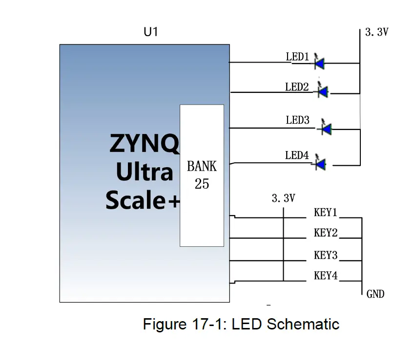
LED and Key Pin Assignment:
| Signal Name | Pin Name | Pin Number |
| LED1 | IO_L9N_24 | W13 |
| LED2 | IO_L12P_24 | Y12 |
| LED3 | IO_L12N_24 | AA12 |
| LED4 | IO_L7N_24 | AB13 |
| KEY1 | IO_L7P_24 | AA13 |
| KEY2 | IO_L1N_24 | AE14 |
| KEY3 | IO_L1P_24 | AE15 |
| KEY4 | IO_L2P_24 | AG14 |
Part 18: System Clock
The board provides reference clocks for the RTC circuit, PS system, and PL logic parts. The RTC clock is 32.768, the PS system clock is 33.3333Mhz, and the PL end clock is 25Mhz. The schematic diagram of the clock circuit design is shown in Figure 18-1: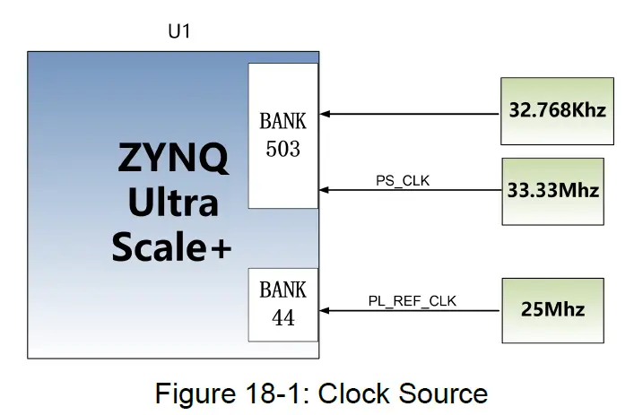
Clock Pin Assignment
| Signal Name | Pin Name | Pin Number |
| PL_REF_CLK | IO_L8P_44 | AB11 |
The level of PL_REF_CLK is +1.8V.
Part 19: ALINX Customized Fan Interface
The fan is powered by 12V, and the speed can be adjusted through the FAN_PWM signal. This board will come with a heatsink in fault, if you need this fan, purchase it separately.
| Signal Name | Pin Name | Pin Number |
| FAN_PWM | IO_L11P_24 | W12 |
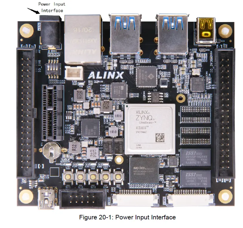
Part 20: Power Input
The power input of AXU2CGA/B is an adapter with DC12V and current 2A. The power interface is shown in the figure below