ALLEGRO A80804 Aid System Designers Demo Board User Manual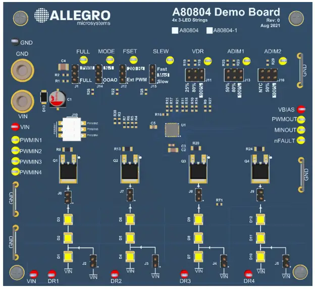
INTRODUCTION
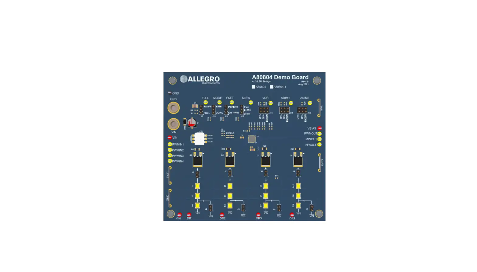
The A80804 demo board is designed to aid system designers with evaluating the operation and performance of Allegro’s A80804 and A80804-1 linear programmable current controllers. The A80804 and A80804-1 are capable of regulating current in four independent LED strings. The A80804 demo board is available in two configurations: one for the A80804 with VSENSE of 500 mV and one for the A80804-1 with VSENSE of 200 mV. The demo board will arrive with a mark on one of the silkscreen boxes in the top right of the demo board to identify which device the demo board was configured for. The demo board has four strings of three white LEDs.
Note: Use caution when powering-on the device as the on-board LEDs are very bright.
Figure 1: A80804 Demo Board
Table 1: A80804 Demo Board Configurations
| Configuration Name | Part Number | VSENSE (mV) | RSENSE (Ω) | ILED (mA) |
| A80804 | APEK80804KET | 500 | 2 | 250 |
| A80804-1 | APEK80804KET-1 | 200 | 0.82 | 240 |
GENERAL SETUP
This section provides an overview of the connections and configuration options of the demo board. Each group of connections highlighted in Figure 2 has a detail section below. The default jumper positions are highlighted in green. The A80804 datasheet contains detailed information on the use and functionality of each pin and should be consulted for more detailed information than is contained in this user manual.
Figure 2: A80804 Demo Board I/O Connections and Default Jumper Positions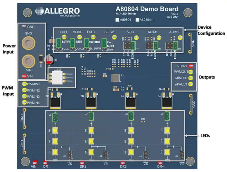
Power Input
Connect a power supply using banana cables to the VIN and GND through-hole banana jack or with test leads to the VIN and GND test points.
LEDs
The LEDs are configured for four independent channels of two or three LEDs in series. Each channel has a jumper which can be used to short-out the first LED in series, and a jumper which can open the LED string to examine fault behavior or monitor the LED current with a series ammeter. The LEDs used in this design are Samsung LM301Z+ 4000K, 400 mA white LEDs, part number SPMWH3326MP7WAT3S0.
PWM Input
The A80804 has four PWM input pins that control the corresponding LED channel. Each channel can be controlled independently or tied together. If the A80804 is configured for internal PWM generation, the PWMINx pins act as enable pins. If the A80804 is configured for external PWM, the PWMINx pins act as the PWM source for each channel. See the FSET section below for configuring the device for internal or external PWM. The 3PDT switch, J10, can optionally connect PWMIN2, PWMIN3, and PMWIN4 to PWMIN1 to minimize the number of input signals required if all PWMINx signals are to be shared.
Device Configuration
There are seven optional configuration jumpers on the demo board to exercise different operating modes of the A80804. Each jumper has a default state when no jumper is installed, indicated on the PCB by the inverted silkscreen text.
Table 2: Default State for Open Jumpers
| Jumper | A80804 Pin | Open State | Description |
| J1 | FULL | PWM | Duty cycle for LED brightness honors PWM configuration |
| J14 | MODE | N-1 | Non-faulted LED strings continue operating normally |
| J12 | FSET | 200 Hz | LED brightness controlled with internal PWM at 200 Hz |
| J15 | SLEW | Med | ILED slew time is configured with a 200 kΩ resistor to GND |
| J11 | VDR | 100% | Internal PWM uses 100% duty cycle |
| J13 | ADIM1 | 100% | LED current is not derated by analog dimming from ADIM1 |
| J16 | ADIM2 | 100% | LED current is not derated by analog dimming from ADIM2 |
UVLO, FDIS, and VINDERAT
The A80804 and A80804-1 demo boards are configured with voltage dividers from VBIAS to configure the UVLO, FDIS, and VINDERAT pins.
Table 3: UVLO, FDIS, and VINDERAT Configuration
| Pin | Description | RTOP (kΩ) | RBOT (kΩ) | Pin Voltage (V) | A80804 Configuration |
| UVLO | VIN Undervoltage Lockout | 10 | 3.92 | 1.4 | Undervoltage Lockout = 7 V |
| FDIS | VIN LED Fault Disable | 10 | 6.65 | 2.0 | LED Faults Disabled when VIN < 10 V |
| VINDERAT | VIN Input Voltage Derating Start | 10 | 6.34 | 1.93 | LED current derates for VIN > 20 V |
FULL
The FULL pin on the A80804, when pulled high, overrides any PWM dimming and forces the LEDs to operate at 100% brightness. Jumper J1 can be installed in either the “PWM” option to pull the FULL pin down and honor the PWM settings for the LED brightness, or the “FULL” option to force 100% duty cycle. If the jumper is not installed at “FULL”, it is pulled down and the A80804 behaves the same as when jumper is the “PWM” option. Operating in FULL mode sets the PWM duty cycle to 100% but does not override any analog dimming.
Table 4: FULL Pin Jumper J1
| J1 State | Effect |
| Open | LED brightness honors current PWM dimming setting |
| PWM | LED brightness honors current PWM dimming setting |
| FULL | LED brightness forced to 100% duty cycle |
MODE
The MODE pin controls the A80804 fault response. Set the MODE jumper, J14, to the “OOAO” option for “one-out-all-out” operation to disable all LEDs when a fault is detected. Set J14 to “N-1” or leave the jumper open to allow non-faulted LED strings to continue to operate normally. Jumpers J6 to J9 can be used to induce LED open faults.
Table 5: MODE Pin Jumper J14
| J14 State | Effect |
| Open | LED strings unaffected by a fault continue to operate |
| N-1 | LED strings unaffected by a fault continue to operate |
| OOAO | All LED strings are disabled when a fault is detected |
FSET
The FSET pin controls the PWM mode of the A80804. Set jumper J12 to the “Ext PWM” option to use external PWM and control each LED string’s brightness individually with the four PWMINx test points. Optionally, the switches in J10 can be used to tie any combination of PWMIN2, PWMIN3, or PWMIN4 to PWMIN1 to reduce the number of external PWM sources needed. Set J12 to the “200 Hz” option to enable internal PWM at 200 Hz. While using internal PWM the PWMINx pins act as LED string enable pins, and the duty cycle is set by VDR, see the VDR section.
Table 6: FSET Pin Jumper J12
| J14 State | Effect |
| Open | A80804 operates with internal PWM at 200 Hz |
| 200 Hz | A80804 operates with internal PWM at 200 Hz |
| Ext PWM | A80804 operates with external PWM using PWMINx pins |
SLEW
The SLEW jumper, J15, controls the slew time of the LED current. Install jumper J15 at the top two pins to select “Fast”, the bottom two pins to select “Slow”, or open the jumper to select “Med”.
Table 7: SLEW Pin Jumper J15
| J15 State | Effect |
| Fast | ILED slew time is 6 µs (typical) |
| Open (Med) | ILED slew time is 50 µs (typical) |
| Slow | ILED slew time is 80 µs (typical) |
VDR
The VDR jumper, J11, controls the duty cycle for the internal PWM generation.
Set jumper J11 to “100%”, “80%”, or “25%” to select the corresponding duty cycle when using internal PWM (FSET installed to “PWM” or open). Leaving J11 open will also select 100% duty cycle.
Table 8: VDR Pin Jumper J11
| J11 State | Effect |
| Open | Internal PWM operates at 100% duty cycle |
| 100% | Internal PWM operates at 100% duty cycle |
| 80% | Internal PWM operates at 80% duty cycle |
| 25% | Internal PWM operates at 25% duty cycle |
ADIM1
The ADIM1 jumper, J13, selects the level of analog dimming to use in order to derate the peak LED current using the ADIM1 pin on the A80804. Set J13 to “100%”, “80%”, or “50%” to select the corresponding level of analog dimming. Leaving jumper J13 open will also select “100%”.
Table 9: ADIM1 Pin Jumper J13
| J13 State | Effect |
| Open | LED current is not derated |
| 100% | LED current is not derated |
| 80% | LED current is derated to 80% of its full value |
| 50% | LED current is derated to 50% of its full value |
ADIM2
The ADIM2 jumper, J16, selects the level of analog dimming to use to derate the peak LED current using the ADIM2 pin on the A80804. Set J16 to “100%” or “50%” to select the corresponding level of analog dimming. Set J16 to “NTC” to derate the LED current based the NTC thermistor RT1 temperature, which is placed between Q3 and Q4; see the NTC Derating section in this document for more information about the temperature derating circuit. Leaving jumper J16 open it will also select “100%”.
Table 10: ADIM2 Pin Jumper J16
| J16 State | Effect |
| Open | LED current is not derated |
| 100% | LED current is not derated |
| 50% | LED current is derated to 50% of its full value |
| NTC | LED current is derated based on the temperature at RT1 |
Outputs
VBIAS
The VBIAS test point can be used to measure the VBIAS rail that is used for several voltage dividers for device configuration. The VBIAS rail is meant to source no more than 10 mA total, including the voltage dividers already on the board.
PWMOUT
The PWMOUT signal represents the signal used by the internal PWM generator and is disabled when the A80804 is configured for external PWM.
MINOUT
The MINOUT signal represents the minimum MOSFET drain voltage of all enabled channels.
NFAULT
The open drain fault flag, nFAULT, will be pulled low when a fault is detected and released when the fault is removed.
GETTING STARTED
The A80804 demo board has LEDs included and arrives ready for use. Apply power with a power supply that can supply more than 1 A to support the LED current for all four channels. Recommended input voltage range while getting started is between 12 and 18 V to fully drive the LEDs and stay under the input voltage derating threshold.
If the jumpers are all open or set in their default positions as defined in Table 2, and the PWMINx pins are left open or pulled high, the device will turn on in internal PWM at 100% duty cycle with no analog dimming, resulting in 250 mA per LED channel.
Warning: Use caution when powering up the board. The LEDs are very bright and will turn on when power is applied to the demo board unless the PWMINx pins are pulled low, VIN is less than the 7 V UVLO threshold, or jumpers J6 to J9 are open.
The three position DIP switch, J10, can be used to connect PWMIN2, PWMIN3 and PWMIN4 to PWMIN1, allowing the PMWIN1 test point to act as a single connection to enable/disable or drive a single PWM source to the PWMINx pins to simplify the connections required. Open any or all the DIP switches to control the related PWMINx pins independently.
The following sections highlight how to set up the board for different applications.
Internal PWM
To operate in internal PWM, see Table 11 for the required jumper positions and see Figure 3 for an example of the remaining jumper positions. Note, only the jumper settings in Table 11 are required for internal PWM; the other jumpers in Figure 3 can be modified.
The PWMINx test points act as LED channel enable signal while operating in internal PWM.
Table 11: Internal PWM Configuration
| Jumper | A80804 Pin | State | Description |
| J1 | FULL | PWM | Duty cycle for LED brightness honors PWM configuration |
| J12 | FSET | 200 Hz | LED brightness controlled with internal PWM at 200 Hz |
Figure 3: A80804 Demo Board I/O Connections and Default Jumper Positions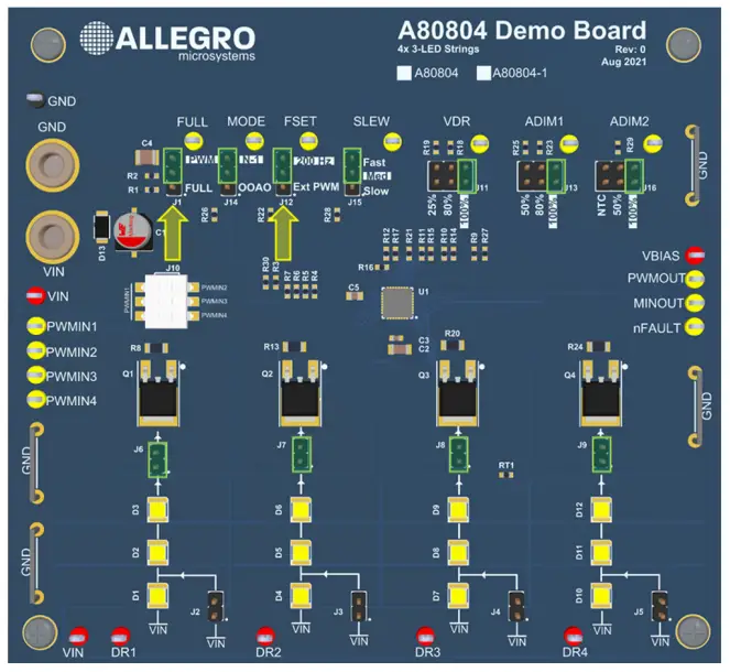
The VDR and ADIMx jumper settings are configured by the user for the desired application. The internal duty cycle can be set with the VDR jumper to 100%, 50%, or 25%. For other internal dimming duty cycles, open the VDR jumper, J11, and apply a voltage source between 0 and 3.6 V to the VDR test point. For example, to set internal PWM duty cycle to 10%, apply 0.34 V to the VDR test point. Refer to the datasheet for more information about configuring internal PWM. See Figure 4 below showing 25% duty cycle on LED channel 1. When analog dimming is used, the peak LED current is derated by the level of analog dimming, as shown in Figure 5 with the ADIM1 jumper installed to the 50% option.
Figure 4: ILED1 with Internal PWM at 25% Duty Cycle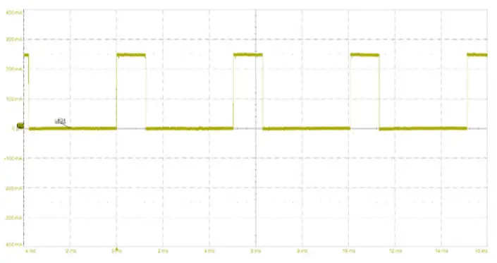
Figure 5: ILED1 with 25% Duty Cycle and 50% Analog Dimming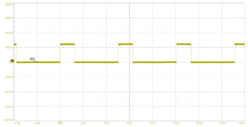
When the FULL pin is pulled high by installing J1 for the “FULL” option, the PWM duty cycle is forced to 100%; the analog dimming level is unaffected.
Figure 6: Toggling the FULL Pin While Dimming At 25% Duty Cycle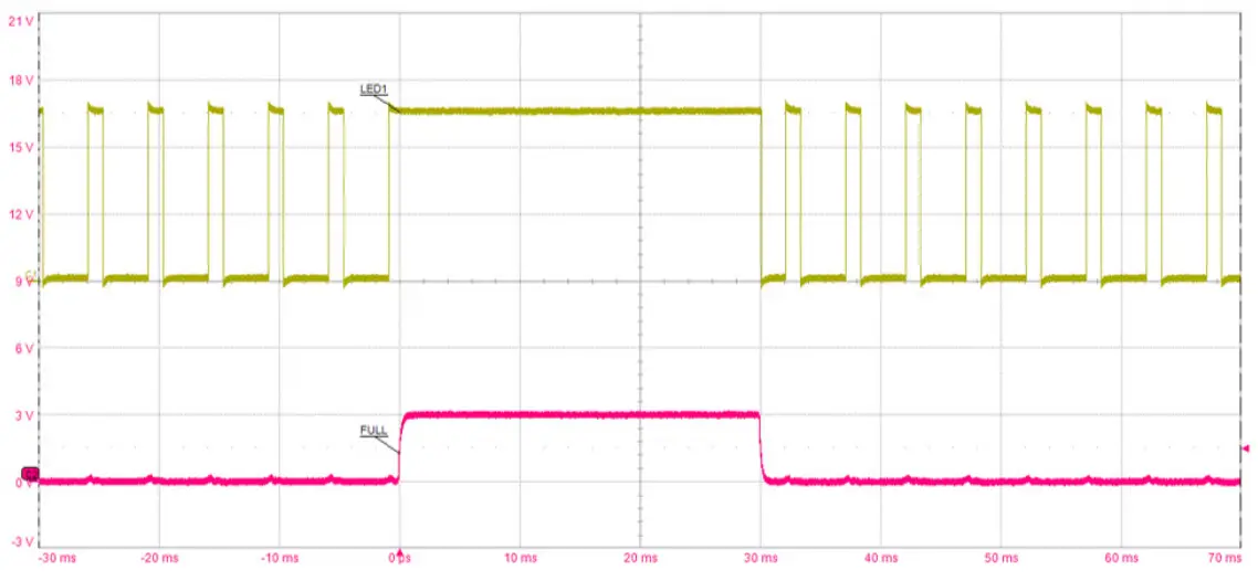
External PWM
To operate in external PWM, see Table 12 for the required jumper positions and see Figure 7 for an example of the remaining jumper positions. Note, the VDR jumper in Figure 7 is ignored when FSET is set for external PWM.
Table 12: External PWM Configuration
| Jumper | A80804 Pin | State | Description |
| J1 | FULL | PWM | Duty cycle for LED brightness honors PWM configuration |
| J12 | FSET | Ext PWM | LED brightness controlled with internal PWM at 200 Hz |
The duty cycle for each LED channel can be independently controlled by applying a PWM signal to each of the four PWMINx test points. If desired, multiple PWMINx test points can be grouped together with PWMIN1 using switch J10 so a single PWM source can drive multiple PWMINx pins.
Figure 7: A80804 Demo Board Configured for External PWM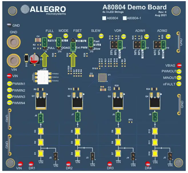
See Figure 8 for an example oscilloscope capture with ILED1 and ILED2 driven with independent PWMIN signals, where LED1 is driven with 10% duty cycle and LED2 is driven with 50% duty cycle.
Figure 8: ILED1 and ILED2 with Independent Duty Cycles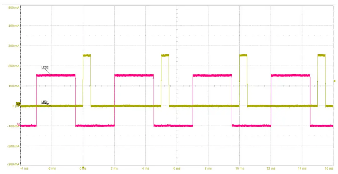
Cascading Multiple Demo Boards
To cascade multiple demo boards together for additional light output, configure a master demo board for internal PWM and a slave demo board for external PWM. Set J10 of the slave demo board so all PWMIN signals are tied to PWMIN1, then tie PWMIN1 to PWMOUT of the master demo board. Optionally, to maintain “one-out-all-out” behavior with multiple A80804 devices, set the MODE jumper on both demo boards to “OOAO” and tie the nFAULT test points together. See Figure 9 for a connection drawing.
Figure 9: Cascading Multiple A80804 Demo Boards Together with PWMOUT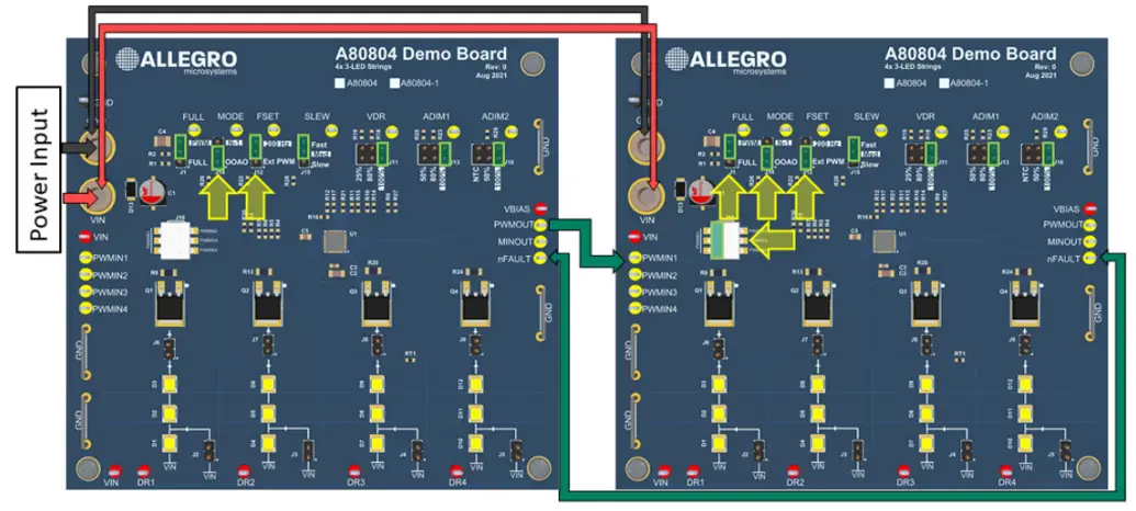
Alternatively, external PWM signals can be synchronized across multiple demo boards when the PWMIN signals are tied to the same external PWM source. Remove the FULL jumper from the slave demo board and tie the FULL test points together to share a common FULL signal. See Figure 10 for a connection diagram.
Figure 10: Cascading Multiple A80804 Demo Boards with Synchronized External PWM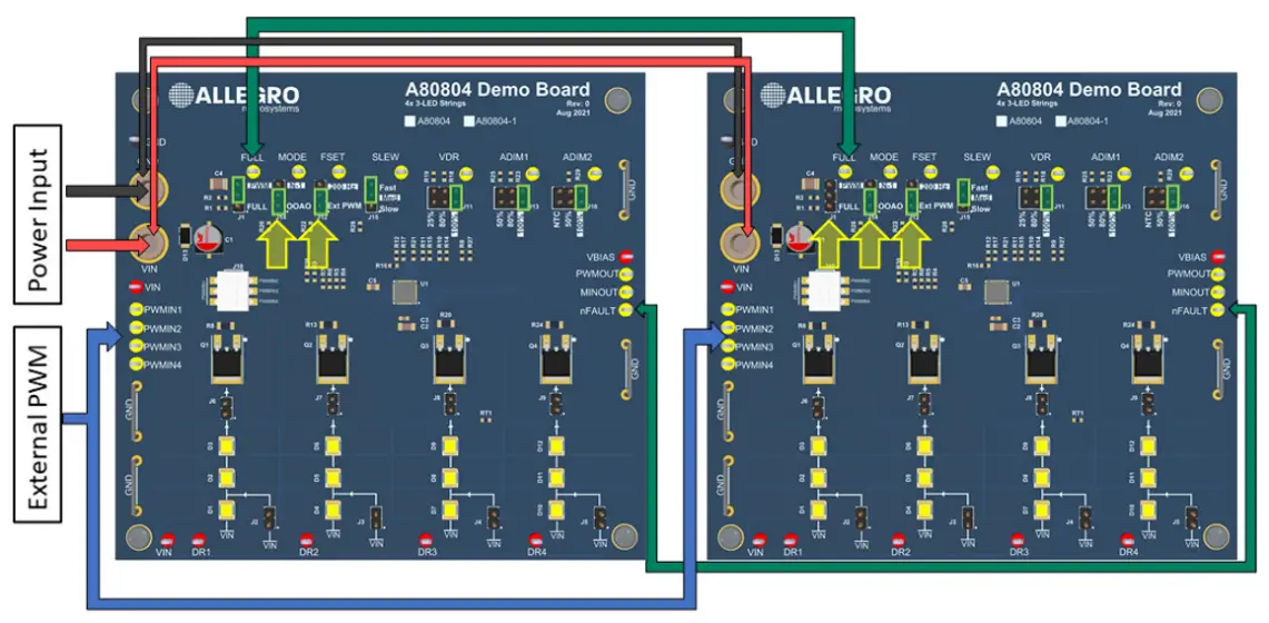
THERMAL MANAGEMENT
The A80804 is a linear MOSFET controller and therefore most of the heat generation occurs within the external MOSFETs and the LEDs. The A80804 Demo Board is designed to operate all four channels at 100% duty cycle at 250 mA over the full input voltage range of the A80804 at room temperature. Large copper areas are added around the MOSFETs and LEDs for heat dissipation. There are also vias in the pad for each MOSFET and LED to the bottom copper layer for additional heat dissipation. The outer layers of the PCB have 2-ounce copper which allows heat to dissipate more efficiently.
Thermal Performance
The following figures show the thermal performance of the A80804 Demo Board at 100% duty cycle and input voltage of 14 V after 10 minutes of continuous operation with ambient temperature near 25°C. The MOSFET drain tabs are the four warm spots across the middle of the image and the LED grid is at the bottom of the image.
Figure 11: A80804 Demo Board Thermal Image at VIN = 14 V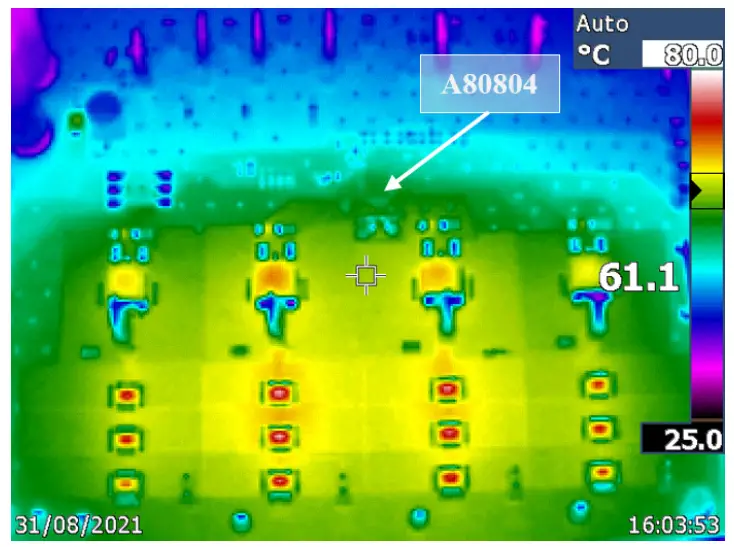
Figure 12: A80804-1 Demo Board Thermal Image at VIN = 14 V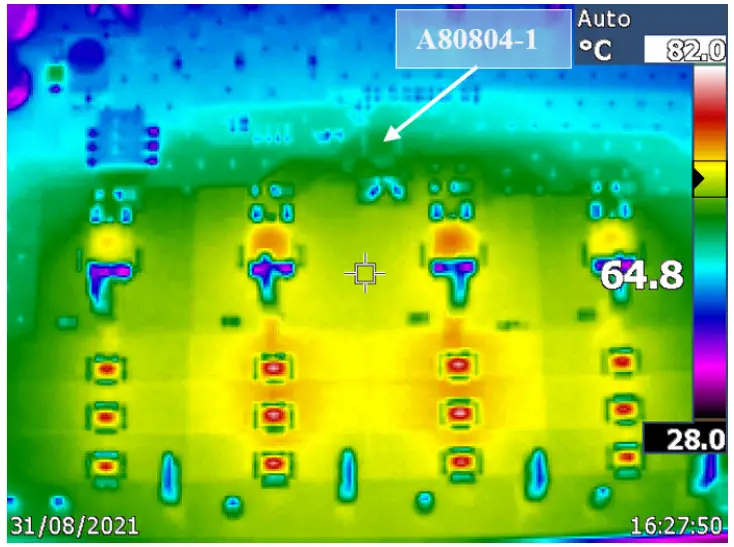
NTC Derating
The A80804 Demo Board is equipped with an NTC thermistor, part number NTCS0603E3104FXT, available on ADIM2, populated on the PCB between MOSFETs Q3 and Q4, highlighted in Figure 13. To use the NTC derating circuit, set jumper J16 to the NTC option. An example jumper configuration is shown in Figure 13. The schematic for the NTC derating circuit is reproduced in Figure 14.
Figure 13: ADIM2 Jumper J16 Installed for NTC Derating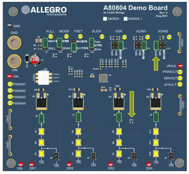
Figure 14: Voltage Divider at ADIM2 when J16 Installed at NTC Option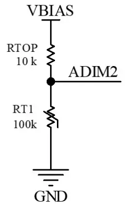
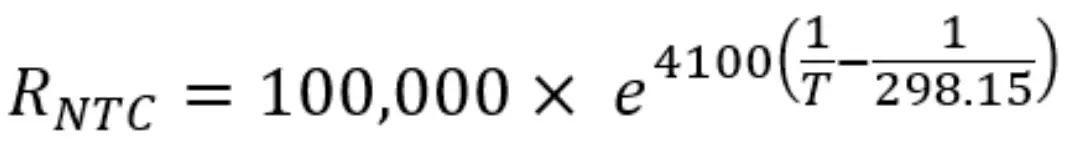
The voltage at the ADIM2 pin with the circuit as shown in Figure 14 changes with temperature as RT1 heats up. The expected derating curve is calculated with: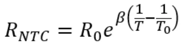
Where:
- RNTC: Thermistor resistance at temperature T
- R0: Thermistor resistance at 25°C
- T: Thermistor temperature in Kelvin
- T0: Thermistor baseline temperature in Kelvin, typically 298.15 K (25°C)
- β: Thermistor 25°C to 85°C Beta Constant (B25/85)

The blue curve in Figure 14 shows the expected voltage at the output of the voltage divider leading to ADIM2, and the yellow curve is the measured data at the ADIM2 test point. Since ADIM2 does not derate until VADIM2 is less than half of VBIAS, or VADIM2 / VBIAS < 0.5 V, the NTC thermal derating using this circuit starts at 85°C, as shown in Figure 15. The percent dimming on the right axis of Figure 15 is the ratio of the VSENSE voltage to the nominal VSENSE voltage of 500 mV.
Figure 14: Voltage at ADIM2 pin Over Temperature with NTC Derating Circuit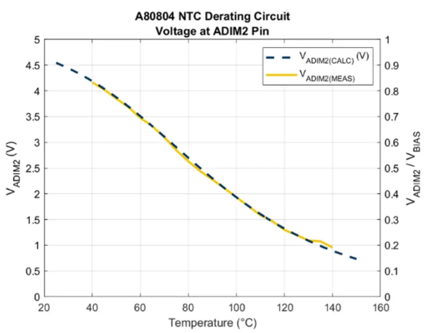
Figure 15: VSENSE and LED Dimming vs. Temperature with NTC Derating Circuit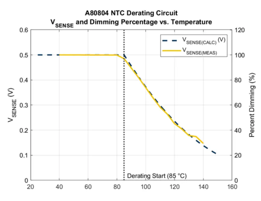
APEK80804KET SCHEMATIC
Figure 16: APEK80803KET Schematic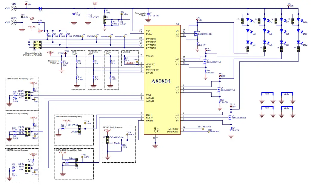
APEK80804KET Bill of Materials
| Designator | Description | Quantity | Manufacturer | Manufacturer P/N |
| U1 | A80804 in QFN-32 | 1 | Allegro MicroSystems | A80804KETASR |
| C1 | Aluminum Electrolytic Capacitor, 47 µF, 50 V, Radial Can, 6.3 mm | 1 | ||
| C2 | Ceramic 2.2 µF 50 V X7R 10% 1206 | 1 | ||
| C3 | Ceramic 0.1 µF 50 V X7R 10% 0603 | 1 | ||
| C4 | Ceramic 3.3 µF 50 V X7R 10% 1210 | 1 | ||
| C5 | Ceramic 2.2 µF 16 V X7R 10% 0805 | 1 | ||
| CN1, CN2 | Banana Jack – Non-Insulated 0.218″ | 2 | Keystone Electronics | 575-4 |
| D1, D2, D3, D4, D5, D6, D7, D8, D9, D10, D11, D12 | LM301Z+ 4000K 400 mA 90CRI | 12 | Samsung | SPMWH3326MP7WAT3S0 |
| D13 | Diode Schottky 60 V 5 A Surface Mount | 1 | Rohm | RB088LAM-60TFTR |
| J1, J12, J14, J15 | CONN HEADER VERT 3POS 2.54 mm | 4 | ||
| J2, J3, J4, J5, J6, J7, J8, J9 | CONN HEADER VERT 2POS 2.54 mm | 8 | ||
| J10 | SWITCH SLIDE DIP SPST 25 mA 24 V | 1 | ITT C&K | SDA03H1SBD |
| J11, J13, J16 | CONN HEADER VERT 6POS 2.54 mm | 3 | ||
| MS1, MS2, MS3, MS4 | PAN HEAD SCREW_M3 × 8 mm CROSS SL | 4 | Wurth Electronics | 97790803111 |
| Q1, Q2, Q3, Q4 | MOSFET N-CH 60 V 8 A TO-252-2 (DPAK) | 4 | Rohm | RD3L080SNTL1 |
| R1, R2, R4, R5, R6, R7, R26 | Resistor, 100 kΩ, 1/8 W, 1%, 0603 | 7 | ||
| R8, R13, R20, R24 | Resistor, 2 Ω, 1/2 W, 1%, 1206 | 4 | ||
| R9, R10, R11, R12, R17, R21 | Resistor, 10 kΩ, 1/10 W, 1%,0603 | 6 | ||
| R14 | Resistor, 6.65 kΩ, 1/10 W 1%, 0603 | 1 | ||
| R15 | Resistor, 6.34 kΩ, 1/10 W, 1%,0603 | 1 | ||
| R16 | Resistor, 3.92 kΩ, 1/10 W, 1%,0603 | 1 | ||
| R18 | Resistor, 12.1 kΩ, 1/10 W, 1%, 0603 | 1 | ||
| R19 | Resistor, 2.05 kΩ, 1/10 W, 1%, 0603 | 1 | ||
| R22 | Resistor, 30.9 kΩ, 1/10 W, 1%, 0603 | 1 | ||
| R23 | Resistor, 17.8 kΩ, 1/10 W, 1%, 0603 | 1 | ||
| R25 | Resistor, 6.65 kΩ, 1/10 W, 1%, 0603 | 1 | ||
| R27 | Resistor, 10 kΩ, 1/10 W, 1%,0603 | 1 | ||
| R28 | Resistor, 200 kΩ, 1/10 W, 1%,0603 | 1 | ||
| R29 | Resistor, 3.83 kΩ, 1/10 W, 1%, 0603 | 1 | ||
| R30 | Resistor, 0 Ω, 1/10 W, 1%, 0603 | 1 | ||
| RT1 | Thermistor NTC 100 kΩ 1% 0603 4100K | 1 | Vishay | NTCS0603E3104FXT |
| STND1, STND2, STND3, STND4 | Standoffs & Spacers 5.0 HEX 15.0mm NYLON | 4 | Keystone Electronics | 25512 |
| TP1, TP2, TP5, TP10, TP11, TP13, TP15 | Test Point, Red, Through Hole Mount, 1.6 mm | 7 | Keystone Electronics | 5010 |
| TP3 | Test Point, Black, Through Hole Mount, 1.6 mm | 1 | Keystone Electronics | 5011 |
| TP4, TP6, TP7, TP8, TP9, TP12, TP14, TP16, TP17, TP18, TP19, TP20, TP21, TP22 | Test Point, Yellow, Through Hole Mount, 1.6 mm | 14 | Keystone Electronics | 5014 |
APEK80804KET-1 SCHEMATIC
Figure 17: APEK80803KET-1 Schematic 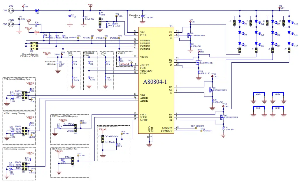
APEK80804KET-1 Bill of Materials
| Designator | Description | Quantity | Manufacturer | Manufacturer P/N |
| U1 | A80804-1 in QFN-32 | 1 | Allegro MicroSystems | A80804KETASR-1 |
| C1 | Aluminum Electrolytic Capacitor, 47 µF, 50 V, Radial Can, 6.3 mm | 1 | ||
| C2 | Ceramic 2.2 µF 50 V X7R 10% 1206 | 1 | ||
| C3 | Ceramic 0.1 µF 50 V X7R 10% 0603 | 1 | ||
| C4 | Ceramic 3.3 µF 50 V X7R 10% 1210 | 1 | ||
| C5 | Ceramic 2.2 µF 16 V X7R 10% 0805 | 1 | ||
| CN1, CN2 | Banana Jack – Non-Insulated 0.218″ | 2 | Keystone Electronics | 575-4 |
| D1, D2, D3, D4, D5, D6, D7, D8, D9, D10, D11, D12 | LM301Z+ 4000K 400 mA 90CRI | 12 | Samsung | SPMWH3326MP7WAT3S0 |
| D13 | Diode Schottky 60 V 5 A Surface Mount | 1 | Rohm | RB088LAM-60TFTR |
| J1, J12, J14, J15 | CONN HEADER VERT 3POS 2.54 mm | 4 | Wurth Electronics | 61300311121 |
| J2, J3, J4, J5, J6, J7, J8, J9 | CONN HEADER VERT 2POS 2.54 mm | 8 | Wurth Electronics | 61300211121 |
| J10 | SWITCH SLIDE DIP SPST 25 mA 24 V | 1 | ITT C&K | SDA03H1SBD |
| J11, J13, J16 | CONN HEADER VERT 6POS 2.54 mm | 3 | Wurth Electronics | 61300621121 |
| MS1, MS2, MS3, MS4 | PAN HEAD SCREW_M3 × 8 mm CROSS SL | 4 | Wurth Electronics | 97790803111 |
| Q1, Q2, Q3, Q4 | MOSFET N-CH 60 V 8 A TO-252-2 (DPAK) | 4 | Rohm | RD3L080SNTL1 |
| R1, R2, R4, R5, R6, R7, R26 | Resistor, 100 kΩ, 1/10 W, 1%, 0603 | 7 | ||
| R8, R13, R20, R24 | Resistor, 0.82 Ω, 1/2 W, 1%, 1206 | 4 | ||
| R9, R10, R11, R12, R17, R21 | Resistor, 10 kΩ, 1/10 W, 1%, 0603 | 6 | ||
| R14 | Resistor, 6.65 kΩ, 1/10 W 1%, 0603 | 1 | ||
| R15 | Resistor, 6.34 kΩ, 1/10 W, 1%, 0603 | 1 | ||
| R16 | Resistor, 3.92 kΩ, 1/10 W, 1%,0603 | 1 | ||
| R18 | Resistor, 12.1 kΩ, 1/10 W, 1%, 0603 | 1 | ||
| R19 | Resistor, 2.05 kΩ, 1/10 W, 1%, 0603 | 1 | ||
| R22 | Resistor, 30.9 kΩ, 1/10 W, 1%, 0603 | 1 | ||
| R23 | Resistor, 17.8 kΩ, 1/10 W, 1%, 0603 | 1 | ||
| R25 | Resistor, 6.65 kΩ, 1/10 W, 1%, 0603 | 1 | ||
| R27 | Resistor, 10 kΩ, 1/10 W, 1%, 0603 | 1 | ||
| R28 | Resistor, 200 kΩ, 1/10 W, 1%,0603 | 1 | ||
| R29 | Resistor, 3.83 kΩ, 1/10 W, 1%, 0603 | 1 | ||
| R30 | Resistor, 0 Ω, 1/10 W, 1%, 0603 | 1 | ||
| RT1 | Thermistor NTC 100 kΩ 1% 0603 4100K | 1 | Vishay | NTCS0603E3104FXT |
| STND1, STND2, STND3, STND4 | Standoffs & Spacers 5.0 HEX 15.0 mm NYLON | 4 | Keystone Electronics | 25512 |
| TP1, TP2, TP5, TP10, TP11, TP13, TP15 | Test Point, Red, Through Hole Mount, 1.6 mm | 7 | Keystone Electronics | 5010 |
| TP3 | Test Point, Black, Through Hole Mount, 1.6 mm | 1 | Keystone Electronics | 5011 |
| TP4, TP6, TP7, TP8, TP9, TP12, TP14, TP16, TP17, TP18, TP19, TP20, TP21, TP22 | Test Point, Yellow, Through Hole Mount, 1.6 mm | 14 | Keystone Electronics | 5014 |
BOARD LAYOUT
Figure 18: Top Layer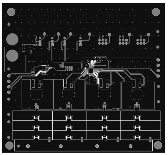
Figure 19: Inner Layer 1 (GND Plane)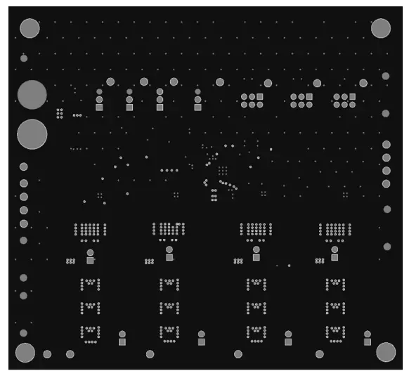
Figure 20: Inner Layer 2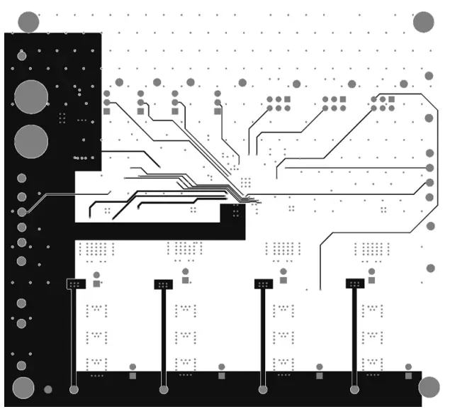
Figure 21: Bottom Layer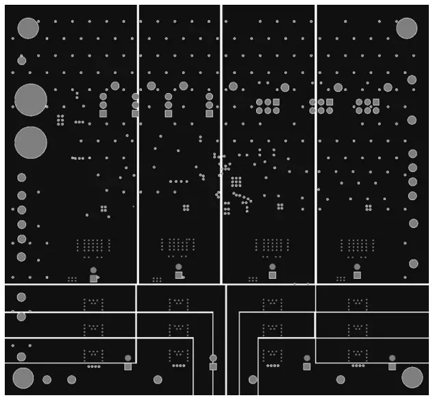
Copyright 2021, Allegro MicroSystems.
Allegro MicroSystems reserves the right to make, from time to time, such departures from the detail specifications as may be required to permit improvements in the performance, reliability, or manufacturability of its products. Before placing an order, the user is cautioned to verify that the information being relied upon is current.
Allegro’s products are not to be used in any devices or systems, including but not limited to life support devices or systems, in which a failure of Allegro’s product can reasonably be expected to cause bodily harm.
The information included herein is believed to be accurate and reliable. However, Allegro MicroSystems assumes no responsibility for its use; nor for any infringement of patents or other rights of third parties which may result from its use.
Copies of this document are considered uncontrolled documents.
Allegro MicroSystems
955 Perimeter Road
Manchester, NH 03103-3353 U.S.A.
www.allegromicro.com