![]() 10W AP3928 EV1 User Guide
10W AP3928 EV1 User Guide
EVB User Guide
Chapter 1. Introduction
General Description
AP3928 is an off-line universal AC Voltage input step-down regulator which provides accurate constant voltage (CV) output, outstanding low standby power, high efficiency at light loading, and excellent dynamic response based on non-isolated buck topology.
The AP3928 EV1 Evaluation Board provides a good design example for a cost-effective 9.9W single output 18V/550mA power application used in home appliances.
AP3928 Key Features
- Universal 85V to 265V VAC Input
- Internal MOSFET 700V (6.5Ω max)
- Maximum 600mA rated Output current
- Low Standby Power Consumption (<30mW at no load)
- High Light-Loading and Average efficiency can meet DOE and CoC requirement
- Frequency Modulation to suppress EMI to meet EN55022 class B
- Rich Protection including OTP, OLP, OLD, SCP
- Extremely low system component count
- Totally Lead-free & Fully RoHS Compliant (SO-8)
- Halogen and Antimony Free. “Green” Device
Applications
- Non-Isolated Home Appliances: AC Fans, Rice Cookers, Air conditioners, Coffee Machines, Soy Milk Machines, etc.
- Auxiliary Power for IoT Devices.
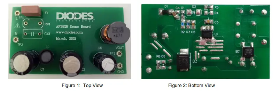
Board Pictures
Chapter 2. Power Supply Specification
System Performance
The system performance contains input/output characters, specifications, EMC, protections, etc.
| Min. | Typ. | Max. | Comments | ||||
| Input Characters | |||||||
| Input AC voltage rating | 100V/60Hz | 115/230 | 240V/50Hz | Two wires, no PE | |||
| Input AC voltage range | 85V/60Hz | – | 265V/50Hz | ||||
| Input AC frequency range | 47Hz | 50/60 | 63Hz | ||||
| Output Characters | |||||||
| Output voltage | 17.1V | 18V | 18.9V | Tested at board terminal | |||
| Output tolerance | ±5% | ||||||
| Loading current | 550 | mA | |||||
| Measurement Performance | |||||||
| Standby power | 16.5mW | Q230V/50Hz | |||||
| Efficiency standard | 115Vac | 10% load | 88.% | – | DoE VI: 71.97% CoC V5 tier 2: 72.03%/62.03% | ||
| Avg. eff. | 87.% | – | |||||
| 230Vac | 10% load | 85.% | |||||
| Avg. eff. | 86.% | ||||||
| Load regulation | ±2.19% | – | Tested at board terminal | ||||
| Line regulation | ±0.28% | – | Tested at board terminal | ||||
| Ripple & Noise | – | 57.6mV | – | Mull load and full voltage range | |||
| Startup time | – | 18.6ms | – | 85V/60Hz | |||
| EMC Test | |||||||
| ESD test | Air | 15kV | – | – | @loon concrete resistor | ||
| Contact | 8kV | – | – | ||||
| EFT test | 2kV | – | – | ±5kHz/100kHz | |||
| Surge Test | 1kV | – | – | Differential mode, 2ohm, 1.2/50us | |||
| Conduction EMI | 110V | 6dB margin | – | – | FCC Part 15 Class B | ||
| 230V | 6dB margin | – | – | EN55022 | |||
| Protection Functions | |||||||
| SCP test | – | – | OK | ||||
| OLD test | – | – | – | OK | |||
| OLP test | 8.2V | – | OK | ||||
| OTP test | 135°C | 150°C | 165°C | OK(IC internal Temp) | |||
Environment
| Operation temperature: | -20°C~85°C |
| Operation Humidity: | 20%~90% R.H. |
| Storage temperature: | 0~40°C |
| Storage Humidity: | 0%~95% R.H. |
Chapter 3. Schematic and Bill of Material
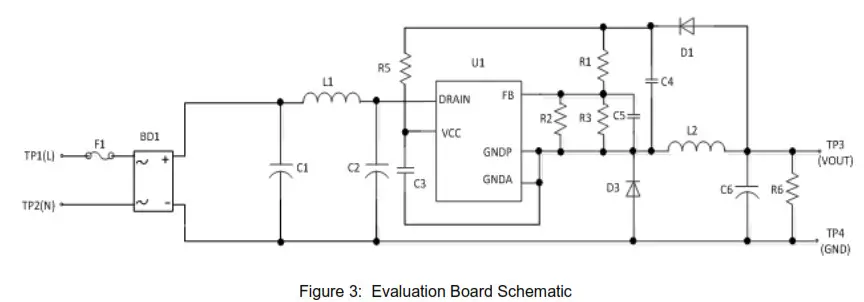
Schematic
Bill of Material
Table 1: Bill of Material
| Items | Designator | Description | Footprint | Qty. | Manufacturer |
| 1 | Ft | 3.15A/300V: Fuse | 8.4*8mm | 1 | OAHE |
| 2 | BD1 | ABS10A | SOPA-4 | 1 | Diodes |
| 3 | C1. C2 | 10uF/400V, Electrolytic capacitor | 010*13mm | 2 | Rubycon |
| 4 | C3 | 2.2pF/25V. X7R | SMD 0805 | 1 | Murata |
| 5 | C4 | 1 pF/50V, X7R | SMD 1206 | 1 | Murata |
| 6 | C5 | 1.5nF/50V, X7R | SMD 0805 | 1 | Murata |
| 7 | C6 | 220pF/35V, Electrolytic capacitor | 08-12rnm | 1 | Rubycon |
| 8 | D1 | RS1MSWF: Fast type diode | SOD123F | 1 | Diodes |
| 9 | D3 | STTH2R06S; Fast diode, 2A/600V | SMC | 1 | ST |
| 10 | L1 | 220pH; Inductor, 0.960, 0.5A | DIP, 05’8mm | 1 | Wurth |
| 11 | L2 | 470pH; Inductor. 0.470. 1.15A | DIP.010’15mm | 1 | Wurth |
| 12 | R1 | 100k0 | SMD 0805, 1% | 1 | Yageo |
| 13 | R2 | 16.2k0 | SMD 0805, 1% | 1 | Yageo |
| 14 | R3 | 300.1k0 | SMD 0805, 1% | 1 | Yageo |
| 15 | R5 | 5.1k0 | SMD 0805, 5% | 1 | Yageo |
| 16 | R6 | 68k0 | SMD 0805, 5% | 1 | Yageo |
| 17 | U1 | AP3928 | SO-8 | 1 | Diodes |
| Total | 18pcs | ||||
Chapter 4. The Evaluation Board Connections
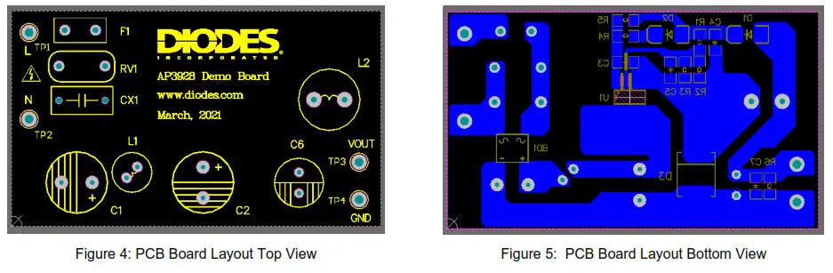
PCB Layout
Circuit Description
4.2.1 Input EMI Filtering
The input stage is composed of fusible resistor F1, rectifier bridge DB1, filtering inductor L1, Capacitors C1 and C2. Resistor F1 is a flame-proof, fusible, wire-wound resistor. It limits inrush current to safe levels for input rectifier diodes, provides differential mode noise reduction and acts as an input fuse in the event of a short circuit.
4.2.2 Control IC
AP3928 co-packages a 700V power MOSFET and control circuitry into a cost-effective SO-8 package. The device is self-starting from the Drain pin with local supply decoupling provided by a small capacitor C3 (at least 100nF) connected to the BP pin when AC source is applied.
4.2.3 Output Rectification
During the ON time of U1, current ramps in L2 and is simultaneously delivered to the load. During the OFF time the inductor current ramps down via the free-wheeling diode D3, feedback diode D1, and the load. Diode D3 should be ultra-fast diodes (Trr<50ns or lower). Capacitor C3 should be selected to have an adequate ripple margin (low ESR type).
4.2.4 Output Feedback
The voltage across L2 is rectified by C4 and D1 during the off-time of U1. For forwarding voltage drop of D1 and D3 is approximately equal, the voltage across C4 tracks the output voltage. To provide a feedback signal, the voltage across C4 is divided by R1 and R2//R3. This voltage is specified for U1 at FB pin (2.5V). This allows the simple feedback to meet the required overall output tolerance of ±5% at rated output current.
4.3 Quick Start Guide
- The evaluation board is preset at 18V/550mA from the output.
- Ensure that the AC source is switched OFF or disconnected before doing connection.
- Connect the AC line wires of the power supply to “L” & “N” connectors on the left side of the board.
- Turn on the AC main switch.
- Measure “+V” & “GND” connectors to ensure correct output voltage, 18V.
CAUTION: This EV board is non-isolated. Do not touch anywhere there are electrical connections because they are all coupled to a high voltage potential.
Chapter 5. System Test
Input & Output Characteristics
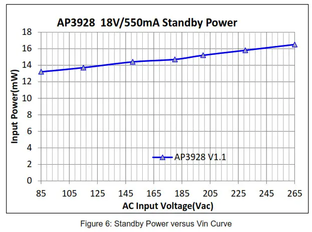
5.1.1 Input Standby Power
Standby power and the output voltage is measured after 10-minute aging. The voltage data is tested at the PCB terminal. All data is tested at ambient temperature.
Table 2: Standby Power and Output Voltage @ no load
| AC Input Voltage | Pin (mW) | Vo (V) |
| 85V/60Hz | 13.2 | 19.025 |
| 115V/60Hz | 13.7 | 19.015 |
| 230V/50Hz | 15.8 | 19.006 |
| 265V/50Hz | 16.5 | 18.999 |
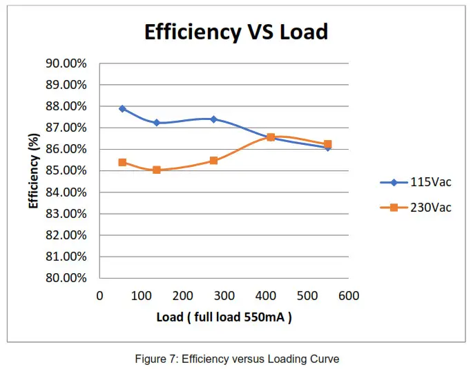
5.1.2 Efficiency
The efficiency data is measured after 10-minute aging, and it is tested at the PCB terminal. All the data is tested at ambient temperature.
Table 3: Conversion Efficiency
| AC Input voltage | Items | 10% | 25% | 50% | 75% | 100% | Avg. Eft |
| 115V/60Hz | Vo (V) | 18.603 | 18.537 | 18.514 | 18.513 | 18.502 | 86.81% |
| Io (mA) | 55 | 137.5 | 275 | 412.5 | 550 | ||
| Pin (W) | 1.0231 | 2.5488 | 5.0913 | 7.6366 | 10.1761 | ||
| Efficiency (% | 87.88% | 87.24% | 87.39% | 86.54% | 86.07% | ||
| 230V/50Hz | Vo (V) | 18.565 | 18.513 | 18.491 | 18.492 | 18.488 | 85.82% |
| Io (mA) | 55 | 137.5 | 275 | 412.5 | 550 | ||
| Pin (W) | 1.0211 | 2.5455 | 5.0851 | 7.6279 | 10.1684 | ||
| Efficiency (% | 85.39% | 85.04% | 85.47% | 86.56% | 86.24% |
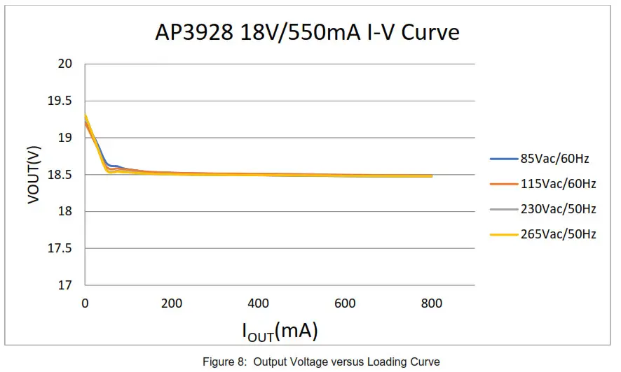
 5.1.3 Line and Load Regulation
The line and load regulation data is measured after 10-minute aging. The voltage data is tested at the PCB terminal. All the data is tested at ambient temperature.
Table 4: Line and Load Regulation Data
| AC input voltage | Loading mA) | ||||||
| 0 | 50 | 100 | 150 | 200 | 250 | 300 | |
| 85Vac/60Hz | 19.215 | 18.654 | 18.572 | 18.532 | 18.524 | 18.516 | 18.512 |
| 115Vac/60Hz | 19.206 | 18.603 | 18.569 | 18.537 | 18.526 | 18.518 | 18.514 |
| 230Vac/50Hz | 19.312 | 18.565 | 18.538 | 18.513 | 18.504 | 18.496 | 18.495 |
| 265Vac/50Hz | 19.315 | 18.556 | 18.530 | 18.512 | 18.505 | 18.501 | 18.498 |
| Line Regulation | ±0.28% | ±0.26% | ±0.11% | ±0.08% | ±0.06% | ±0.06% | ±0.05% |
| AC input voltage | Loading(mA) | Load Regulation | CV Regulation | ||||
| 350 | 400 | 450 | 500 | 550 | |||
| 85Vac/60Hz | 18.503 | 18.494 | 18.489 | 18.485 | 18.483 | ±1.94% | ±4.05% |
| 115Vac/60Hz | 18.513 | 18.511 | 18.509 | 18.506 | 18.502 | ±1.87% | |
| 230Vac/50Hz | 18.493 | 18.492 | 18.491 | 18.489 | 18.488 | ±2.18% | |
| 265Vac/50Hz | 18.495 | 18.493 | 18.491 | 18.488 | 18.487 | ±2.19% | |
| Line Regulation | ±0.05% | ±0.05% | ±0.06% | ±0.06% | ±0.05% | – | |
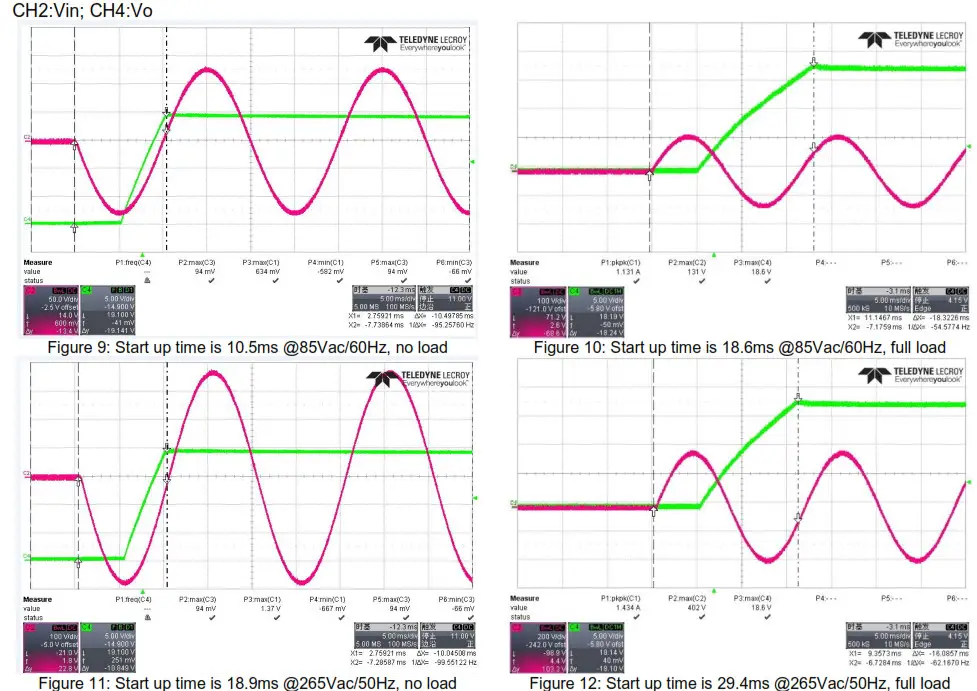
Key Performance Test
5.2.1 Start-up Performance
The start-up time is measured with a differential probe across AC inputs, “L” and “N” connectors, and a common low-voltage probe across output terminals, “+V” and “GND” connectors. Before starting up, buck capacitors should be discharged.
Table 5: Start-up Performance
| AC input voltage | Loading conditions | Figures | |
| No-load | Full load | ||
| 85Vac/60Hz | 10.5ms | 18.6ms | Fig. 9, Fig. 10 |
| 115Vac/60Hz | 10.4ms | 17.9ms | – |
| 230Vac/50Hz | 10.2ms | 16.5ms | – |
| 265Vac/50Hz | 10.1ms | 16.1ms | Fig. 11, Fig. 12 |
CH2:Vin; CH4:Vo
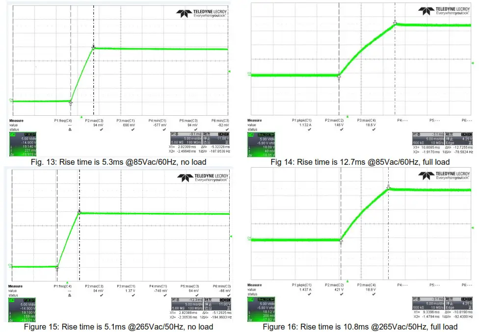
5.2.2 Rise Time
The rise time is measured with a common low-voltage probe across output terminals, “+V” and “GND” connectors. Before starting up, output capacitors should be discharged.
Table 6: Rise Time
| AC input voltage | Loading conditions | Figures | |
| No-load | Full load | ||
| 85Vac/60Hz | 5.3ms | 12.7ms | Fig. 13, Fig.14 |
| 115Vac/50Hz | 5.3ms | 12.4ms | – |
| 230Vac/50Hz | 5.1ms | 11.2ms | – |
| 265Vac/50Hz | 5.1ms | 10.8ms | Fig. 15, Fig.16 |
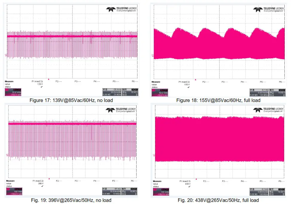
5.2.3 Voltage Stress
The voltage is measured between the “Drain” and “S” pins of AP3928. The test needs differential probes.
Table 7: Internal MOSFET Drain-Source Voltage Stress
| AC input voltage | Loading conditions | Figures | |
| No-load | Full load | ||
| 85Vac/60Hz | 139V | 155V | Fig. 17, Fig 18 |
| 115Vac/60Hz | 184V | 197V | – |
| 230Vac/50Hz | 358V | 364V | – |
| 265Vac/50Hz | 396V | 438V | Fig. 19, Fig. 20 |
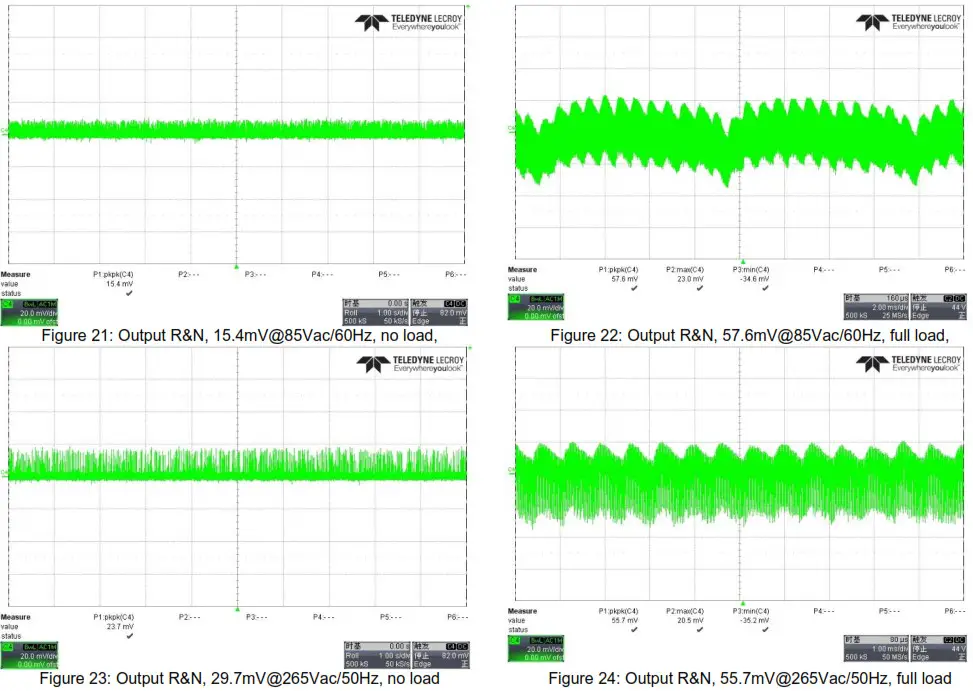
5.2.4 Output Ripple & Noise
The ripple and noise is tested at PCB terminal, using a 10:1 probe without probe cap and ground clip. The bandwidth is limited to 20MHz. A 10µF electrolytic capacitor and a 100nF ceramic capacitor should be paralleled to the output terminal.
Table 8: Ripple & Noise
| AC input voltage | Loading conditions | Figures | |
| No load | Full load | ||
| 85Vac/60Hz | 15.4mV | 57.6mV | Fig. 21, Fig.22 |
| 115Vac/60Hz | 25.5mV | 56.9mV | – |
| 230Vac/50Hz | 27.8mV | 55.2mV | – |
| 265Vac/50Hz | 29.7mV | 55.7mV | Fig. 23, Fig. 24 |
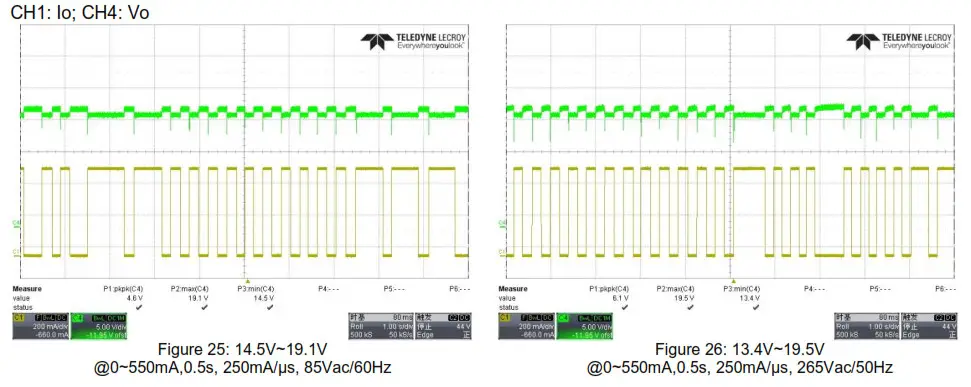
5.2.5 Dynamic Response
The dynamic response of output voltage is tested at the PCB terminal and the bandwidth is limited to 20MHz. Loading is set 0A as low load and 550mA as high load. Besides, the period is 2 seconds and the ramp is set at 250mA/µs.
Table 9: Dynamic Response
| AC input voltage | Output voltage | Figures | |
| Max Vo(V) | Min Vo(V) | ||
| 85Vac/60Hz | 19.1 | 14.5 | Fig. 25 |
| 115Vac/60Hz | 19.2 | 14.6 | – |
| 230Vac/50Hz | 19.4 | 13.9 | – |
| 265Vac/50Hz | 19.5 | 13.4 | Fig. 26 |
Protection Test
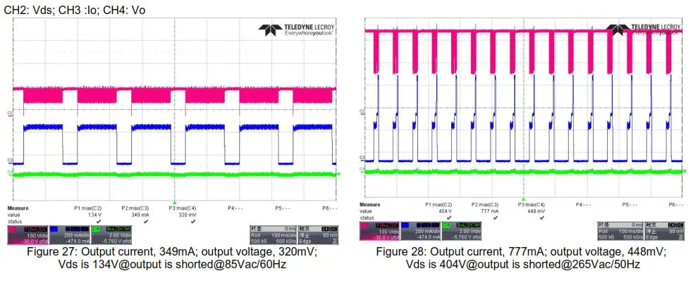
5.3.1 Short Circuit Protection (SCP) Test
The SCP test is measured under the condition that output cable terminals are shorted. The cable end short resistance value used is 50mΩ.
Table 10: Short Circuit Protection Test
| AC input voltage | Max Vo (mV) | Max Io(mA) | Vds(V) | Average input power (W) | Figures |
| 85Vac/60Hz | 320 | 349 | 134 | 0.48 | Fig. 27 |
| 115Vac/60Hz | 320 | 364 | 179 | 0.698 | – |
| 230Vac/50Hz | 448 | 694 | 352 | 0.442 | – |
| 265Vac/50Hz | 448 | 777 | 404 | 0.234 | Fig. 28 |
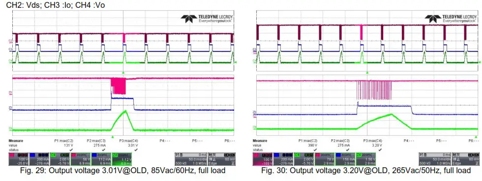
5.3.2 Open Loop Detection (OLD) Protection Test
The open-loop detection protection is measured when FB pin is connected to the Source pin.
Table 11: Open Loop Detection Test
| AC input voltage | The peak of output voltage(V) | Figures |
| 85Vac/60Hz | 3.01 | Fig. 29 |
| 115Vac/60Hz | 3.07 | – |
| 230Vac/50Hz | 3.2 | – |
| 265Vac/50Hz | 3.2 | Fig. 30 |
5.3.3 Overload Protection (OLP) Test
The overload protection point is tested as below: increase the loading by 10mA/step until the system cannot maintain a stable output, and then mark the loading level as overload protection point.
Table 12: Overload Protection Point test
| AC input voltage | Overload protection point(mA) |
| 85Vac/60Hz | 750 |
| 115Vac/60Hz | 750 |
| 230Vac/50Hz | 750 |
| 265Vac/50Hz | 750 |
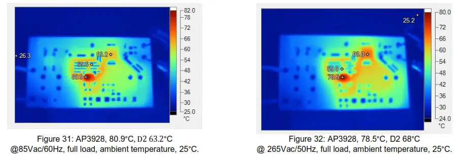
Thermal Test
The thermal test is under ambient temperature after 1-hour aging. The board has no case in open frame. The thermal imager is used to observe the surface temperature of AP3928.

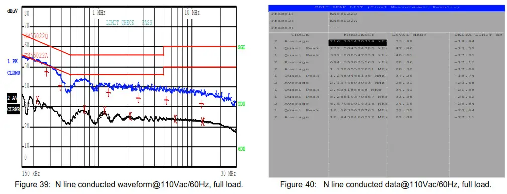
System EMI Scan
The power supply meets EN55022 Class B (for 110Vac input and 230Vac input) EMI requirements with more than 6dB margin.
5.5.1 Conducted EMI Test of 230V@full load
The test result can pass the EN55022 Class B limit with more than 6dB margin.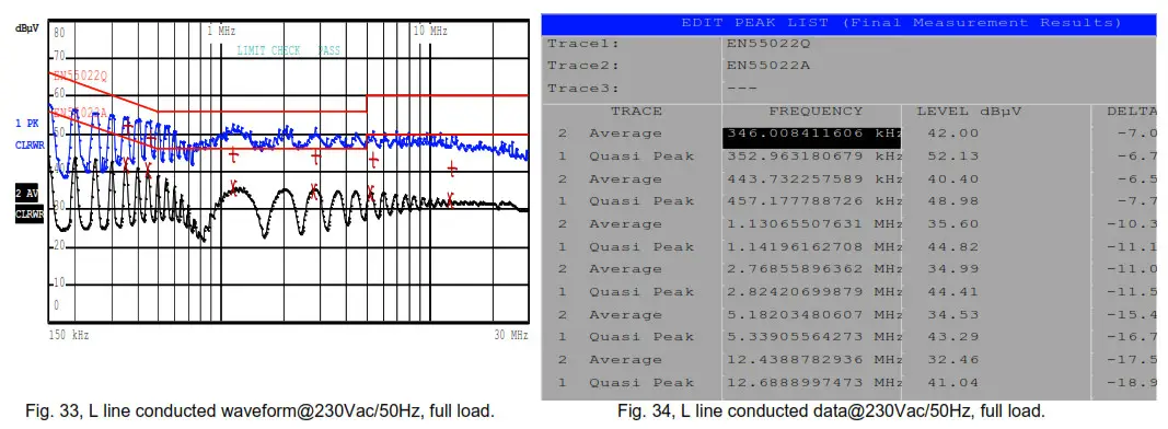
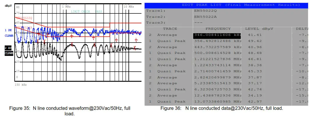
5.5.2 Conducted EMI Test of 110V@full load
The test result can pass the EN55022 Class B limit with more than 6dB margin.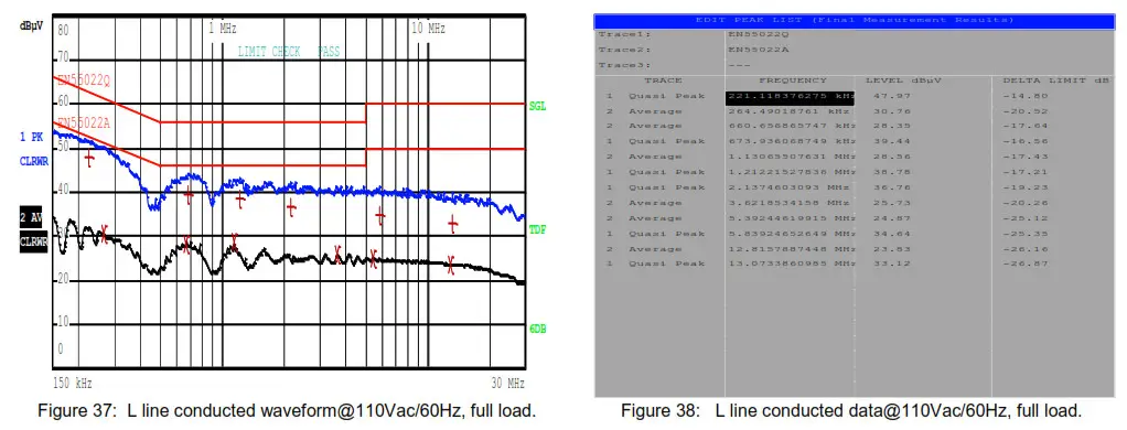
IMPORTANT NOTICE
- DIODES INCORPORATED AND ITS SUBSIDIARIES (“DIODES”) MAKE NO WARRANTY OF ANY KIND, EXPRESS OR IMPLIED, WITH REGARDS TO ANY INFORMATION CONTAINED IN THIS DOCUMENT, INCLUDING, BUT NOT LIMITED TO, THE IMPLIED WARRANTIES OF MERCHANTABILITY, FITNESS FOR A PARTICULAR PURPOSE OR NON-INFRINGEMENT OF THIRD PARTY INTELLECTUAL PROPERTY RIGHTS (AND THEIR EQUIVALENTS UNDER THE LAWS OF ANY JURISDICTION).
- The Information contained herein is for informational purposes only and is provided only to illustrate the operation of Diodes products described herein and application examples. Diodes does not assume any liability arising out of the application or use of this document or any product described herein. This document is intended for skilled and technically trained engineering customers and users who design with Diodes products. Diodes products may be used to facilitate safety-related applications; however, in all instances, customers and users are responsible for (a) selecting the appropriate Diodes products for their applications, (b) evaluating the suitability of the Diodes products for their intended applications, (c) ensuring their applications, which incorporate Diodes products, comply the applicable legal and regulatory requirements as well as safety and functional-safety related standards, and (d) ensuring they design with appropriate safeguards (including testing, validation, quality control techniques, redundancy, malfunction prevention, and appropriate treatment for aging degradation) to minimize the risks associated with their applications.
- Diodes assumes no liability for any application-related information, support, assistance or feedback that may be provided by Diodes from time to time. Any customer or user of this document or products described herein will assume all risks and liabilities associated with such use, and will hold Diodes and all companies whose products are represented herein or on Diodes’ websites, harmless against all damages and liabilities.
- Products described herein may be covered by one or more United States, international or foreign patents and pending patent applications. Product names and markings noted herein may also be covered by one or more United States, international or foreign trademarks and trademark applications. Diodes does not convey any license under any of its intellectual property rights or the rights of any third parties (including third parties whose products and services may be described in this document or on Diodes’ website) under this document.
- Diodes products are provided subject to Diodes’ Standard Terms and Conditions of Sale (https://www.diodes.com/about/company/terms-and-conditions/terms-and-conditions-of-sales/) or other applicable terms. This document does not alter or expand the applicable warranties provided by Diodes. Diodes do not warrant or accept any liability whatsoever in respect of any products purchased through unauthorized sales channels.
- Diodes products and technology may not be used for or incorporated into any products or systems whose manufacture, use or sale is prohibited under any applicable laws and regulations. Should customers or users use Diodes products in contravention of any applicable laws or regulations, or for any unintended or unauthorized application, customers and users will (a) be solely responsible for any damages, losses or penalties arising in connection therewith or as a result thereof, and (b) indemnify and hold Diodes and its representatives and agents harmless against any and all claims, damages, expenses, and attorney fees arising out of, directly or indirectly, any claim relating to any noncompliance with the applicable laws and regulations, as well as any unintended or unauthorized application.
- While efforts have been made to ensure the information contained in this document is accurate, complete and current, it may contain technical inaccuracies, omissions and typographical errors. Diodes does not warrant that information contained in this document is error-free and Diodes is under no obligation to update or otherwise correct this information. Notwithstanding the foregoing, Diodes reserves the right to make modifications, enhancements, improvements, corrections or other changes without further notice to this document and any product described herein. This document is written in English but may be translated into multiple languages for reference. Only the English version of this document is the final and determinative format released by Diodes.
- Any unauthorized copying, modification, distribution, transmission, display, or other use of this document (or any portion thereof) is prohibited. Diodes assume no responsibility for any losses incurred by the customers or users or any third parties arising from any such unauthorized use.
Copyright © 2021 Diodes Incorporated www.diodes.com
www.didoes.com
© Diodes Incorporated


