![]() 100W PFC+QR+GaN PD3.0 Adapter
100W PFC+QR+GaN PD3.0 Adapter
EVB1 User Guide
Summary
General Description
The 100W PD3.0 Evaluation Board (EVB1) is composed of four main controllers, AP33510, APR349, AP43771V and UCC28056B (TI). The AP33510, a highly integrated QuasiResonant (QR) controller with direct Enhancement-mode Gallium Nitride (E-Gann) driver integration, is optimally designed to meet ultra-low standby power and high power density (HPD) charger applications. The APR349, a secondary side synchronous rectifier (SR) controller, is adopted for efficiency optimization. The AP43771V, a PD3.0 PPS protocol controller, automatically manages the PD3.0 PPS attachment process for the attached USB Type C ® -equipped device under charge (DUC), regulates the feedback information of the charger to fulfill voltage and current requirements from DUC. By adopting growing popularity of E-Gann FETs, the 100W EVB1 exemplifies HPD charger design with system BOM optimization to meet market trend.
Key Features
1.2.1 System Key Features
- Quasi-Resonant operation for Critical E-GaN switch Operation and Efficiency Improvement Approaches
- Cost-Effective Implementation for HPD Chargers
- High-Voltage Startup low standby power (<20mW)
- Meets DOE VI and COC Tier 2 Efficiency Requirements
- USB Type-C Port – Support the Maximum Output of 100W PD3.0 PPS (3.3V to 21V@20mV/step, 50mA/step)
- SSR Topology Implementation with an Opto-coupler for Accurate Step Voltage / Current Control
- Low overall system BOM cost
1.2.2 AP33510 Key Features
- QR Fullback Topology with Valley-on and Valley lock
- High-Voltage Startup
- Embedded VCC LDO for VCCIN pin to Guarantee Wide Range Output Voltage
- Integration of Accurate E-Gann direct-driver
- Low Constant Output Current for Output Short
- Non-Audible-Noise QR Control
- Soft Start During Startup Process
- Frequency Foldback for High Average Efficiency
- Secondary Winding Short Protection with FOCP
- Frequency Dithering for Reducing EMI
- Integration of X-CAP Discharge Function
- Useful Pin fault protection: SENSE Pin Floating Protection/FB/Opto-Coupler Open/Short Protection
- Comprehensive System Protection Feature: VOVP/OLP/BNO/SOVP/SUVP
1.2.3 APR349 Key Features
- SR Works with CCM / DCM / QR operation modes
- Eliminate Resonant Ringing Interference
- Fewest External Components used
1.2.4 AP43771V Key Feature
- Support USB PD Rev 3.0 V1.2
- USB-IF PD3.0/PPS Certified TID 4312
- Qualcomm® Quick Charge™ 5 Certified: QC20201127203
- MTP for System Configuration
- OTP for Main Firmware
- Operating Voltage Range: 3.3V to 21V
- Built-In Regulator for CV and CC Control
- Programmable OVP/UVP/OCP/OTP
- Support Power Saving Mode
- External N-MOSFET Control for VBUS Power Delivery
- Supports E-Marker Cable Detection
- QFN-14 and QFN-24
1.3 Applications
- Quick Charger with PD3.0
1.4 Main Power Specifications
| Parameter | Value |
| Input Voltage | 90VAC to 264VAC |
| Input standby power | < 50mW@230VAC/50Hz |
| Main Output (Vo / Io) | PDO: 5V/3A, 9V/3A, 15V/3A, 20V/5A, |
| Efficiency | Comply with CoC version 5 tier-2 |
| Total Output Power | 100W (at PDO 20V/3.25A) |
| Protections | OCP, OVP, UVP, OLP, OTP, SCP |
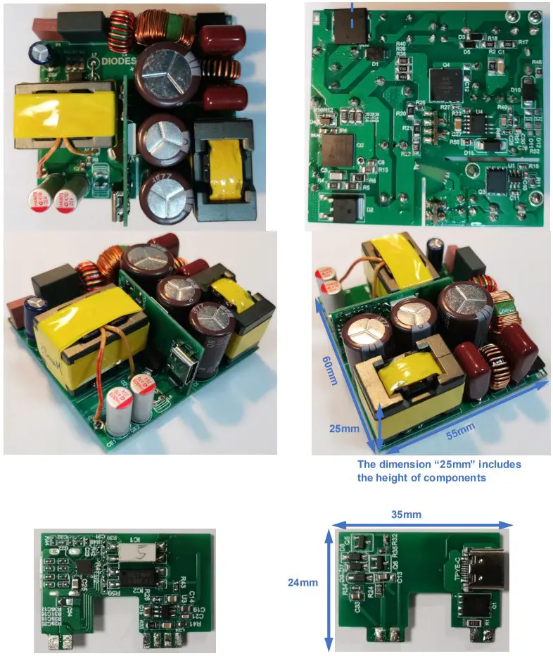
| Dimensions | PCB: 60 * 55 * 25 mm3, 2.362” * 2.165” * 0.984” inch3 |
| Power Density Index | 1.25 W/CC; 20.48 W/CI |
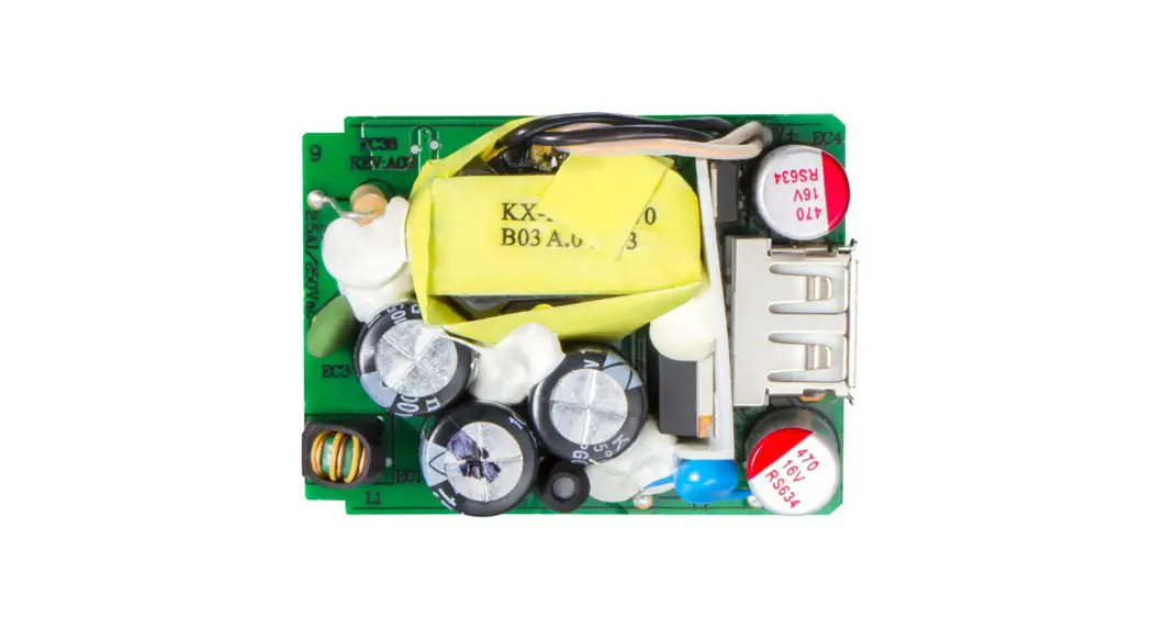
1.5 Evaluation Board Pictures
Power Supply Specification
Specification and Test Results
| Parameter | Value | Test Summary |
| Input Voltage / Frequency | 90VAC to 264VAC / 50Hz or 60Hz | Test Condition |
| Input Current | <2ARMS | |
| Standby Power | < 50mW, load disconnected | PASS, 45mW@230VAC/50Hz |
| 5V/3A Average Efficiency | Choc Version 5, Tier-2 Efficiency >81.84% | PASS, 91.88@115VAC/60Hz 89.74@230VAC/50Hz |
| 5V/0.3A Efficiency (10% Load) | CoCr Version 5, Tier2 Efficiency >72.48% | PASS, 89.77@115VAC/60Hz 85.70@230VAC/50Hz |
| 9V/3A Average Efficiency | CoCr Version 5,Tier2 Efficiency >87.30% | PASS, 92.93@115VAC/60Hz 91.94@230VAC/50Hz |
| 9V/0.3A Efficiency (10% Load) | CoCr Version 5,Tier2 Efficiency >77.30% | PASS, 91.19@115VAC/60Hz 87.98@230VAC/50Hz |
| 15V/3A Average Efficiency | CoCr Version 5,Tier2 Efficiency >88.85% | PASS, 92.94@115VAC/60Hz 92.62@230VAC/50Hz |
| 15V/0.3A Efficiency (10% Load) | Choc Version 5,Tier2 Efficiency >78.85% | PASS, 90.06@115VAC/60Hz 87.48@230VAC/50Hz |
| 20V/5A Average Efficiency | Choc Version 5,Tier2 Efficiency >89% | PASS, 92.69@115VAC/60Hz 93.43@230VAC/50Hz |
| 20V/0.5A Efficiency (10% Load) | CoCr Version 5,Tier2 Efficiency >79% | PASS, 91.09@115VAC/60Hz 89.80@230VAC/50Hz |
| Output Voltage Regulation Tolerance | +/- 5% | PASS, |
Compliance
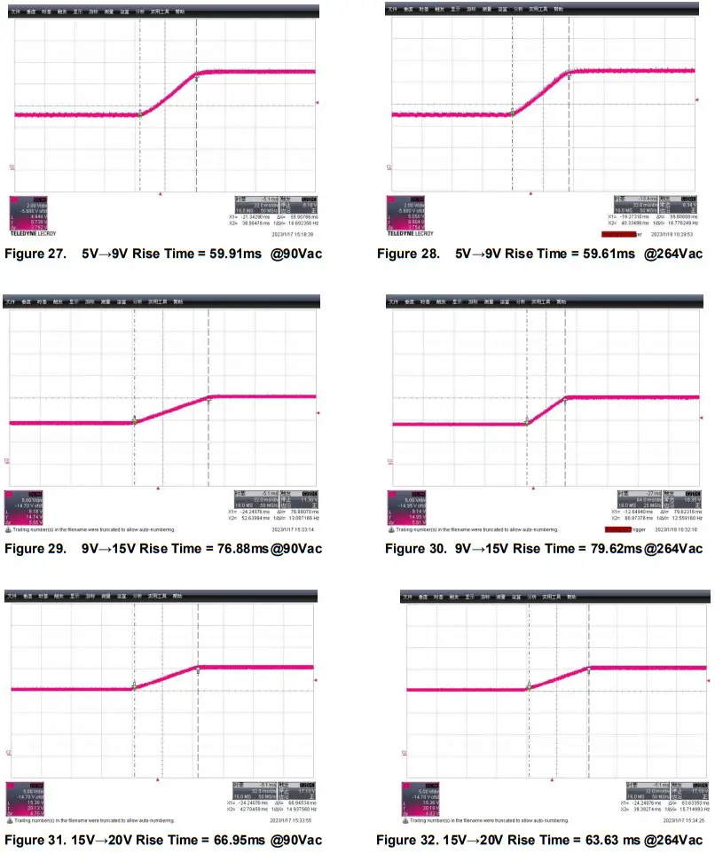
| Parameter | Test conditions | Low to High | High to Low | standard | Test Summary |
| Output Voltage Transition time | 5V/3A to 9V/3A, 90Vac/60Hz | 59.91ms | 60.44ms | 275ms < | Pass |
| 5V/3A to 9V/3A, 264Vac/50Hz | 59.61ms | 66.24ms | Pass | ||
| 9V/3A to 15V/3A, 90Vac/60Hz | 76.88ms | 78.60ms | Pass | ||
| 9V/3A to 15V/3A, 2640Vac/50Hz | 79.62ms | 81.15ms | Pass | ||
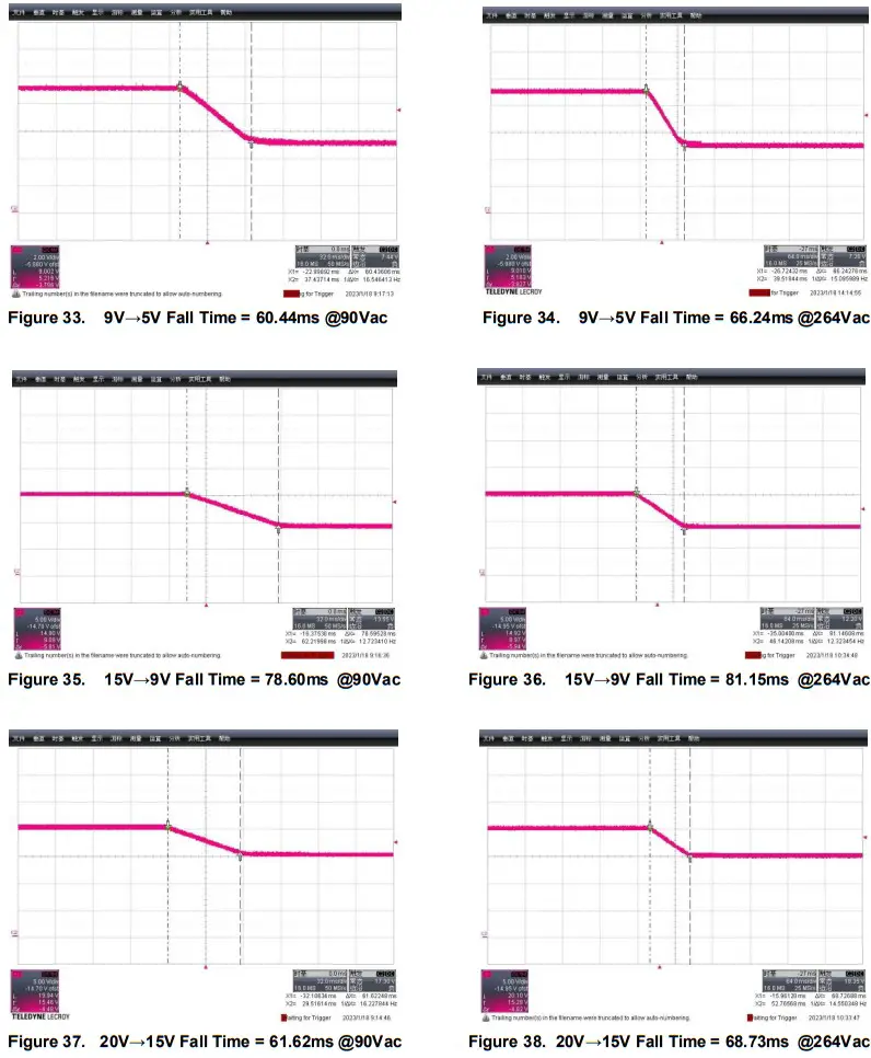
| 15V/3A to 20V/3A, 90Vac/60Hz | 66.95ms | 61.62ms | Pass | ||
| 15V/3A to 20V/3A, 264Vac/50Hz | 63.36ms | 68.73ms | Pass | ||
| USB Type-C *1- | |||||
| 90Vac , Full Load | |||||
| Output Connector | L46mm x 46mm x 22mm (with foldable AC pin) | ||||
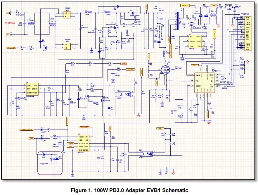
Schematic
Board Schematic
Bill of Material (BOM)
| Item | Quantity | Reference | Description | Manufacturer |
| 1 | 1 | U1 | APR349 | Diodes Incorporated (Diodes) |
| 2 | 1 | U2 | AP43771 | Diodes |
| 3 | 1 | U3 | UCC28056B | TI |
| 4 | 1 | U4 | AP35510 | Diodes |
| 5 | 1 | TPYE-C | TYPE-C | |
| 6 | 1 | R8 | 30K 0603_R | fenghua |
| 7 | 3 | R7, R9, R53 | 39R 1206_R | fenghua |
| 8 | 1 | R55 | 2R 0805_R | fenghua |
| 9 | 1 | R51 | 15K 0603_R | fenghua |
| 10 | 1 | R49 | 220K 0603_R | fenghua |
| 11 | 1 | R48 | BEAD 0805_R | muRata(村田) |
| 12 | 1 | R47 | 1.6K 0402_R | fenghua |
| 13 | 1 | R46 | 300R 0603_R | fenghua |
| 14 | 1 | R44 | 100R 0402_R | fenghua |
| 15 | 1 | R42 | 2k 0402_R | fenghua |
| 16 | 1 | R41 | 61.9k 0603_R | fenghua |
| 17 | 3 | R4, R5, R6 | 3M1206_R | fenghua |
| 18 | 3 | R38, R39, R40 | 0.56R 1206_R | fenghua |
| 19 | 1 | R37 | 470K 0402_R | fenghua |
| 20 | 2 | R35, R43 | 180K 0603_R | fenghua |
| 21 | 1 | R33 | 1K 0805_R | fenghua |
| 22 | 1 | R32 | 750K 0603_R | fenghua |
| 23 | 3 | R30, R45, R50 | 4.7K 0402_R | fenghua |
| 24 | 2 | R3, R24 | 10R 0805_R | fenghua |
| 25 | 4 | R28, R29, R31, R36 | 20R 0402_R | fenghua |
| 26 | 1 | R27 | 10K 0603_R | fenghua |
| 27 | 1 | R26 | 82K 0603_R | fenghua |
| 28 | 1 | R25 | 300K 0603_R | fenghua |
| 29 | 1 | R23 | 15R 0603_R | fenghua |
| 30 | 1 | R22 | 3M6 1206_R | fenghua |
| 31 | 1 | R21 | 3M 1206_R | fenghua |
| 32 | 1 | R20 | 2M7 1206_R | fenghua |
| 33 | 1 | R2 | 330K 1206_R | fenghua |
| 34 | 1 | R19 | 33K 0603_R | fenghua |
| 35 | 2 | R17, R18 | 20K 1206_R | fenghua |
| 36 | 2 | R15, R16, R14 | 0.33R 1206_R | fenghua |
| 37 | 1 | R13 | 22K 1206_R | fenghua |
| 38 | 1 | R11 | 20R 0805_R | fenghua |
| 39 | 2 | R10, R34 | 2.2R 0603_R | fenghua |
| 40 | 1 | R1 | 10mR 1206_R | YAGE |
| 41 | 2 | Q5, Q6 | 2N7002 SOT23_B | Diodes |
| 42 | 1 | Q4 | INN650D260A DFN8*8 | InnoScience |
| 43 | 1 | Q3 | DMT10H045 DFN5*6 | Diodes |
| 44 | 1 | Q2 | TP65H300G4LSG | Transport |
| 45 | 1 | Q1 | TH43M8LS DFN5*6 | Diodes |
| 46 | 1 | L6 | 20uHRING_D9.8 | SANCI |
| 47 | 1 | L5 | 40mHEMC_14*8.5 SQ1010 | SANCI |
| 48 | 1 | L4 | 150uHRING_D9.8 | SANCI |
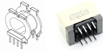
| 49 | 1 | L3 | 320uH ATQ2516 | |
| 50 | 1 | L2 | 200uH ATQ2315 | |
| 51 | 1 | L1 | 100uHLS_D10 | SANCI |
| 52 | 2 | IC1, IC2 | HK1010HCU | Liteon |
| 53 | 1 | F1 | Fuse 3.15A_250V | JDTfuse |
| 54 | 1 | D8 | 20V_1/2W_MINI-MELF SOD_123_B | Diodes |
| 55 | 1 | D9 | 10V_1/2W_MINI-MELF SOD_123_B | Diodes |
| 56 | 1 | D6 | RS1M SMA | Diodes |
| 57 | 2 | D4, D7 | 1N4148 SOD-123(W) | Diodes |
| 58 | 2 | D3, D5 | S1M SMA | Diodes |
| 59 | 1 | D2 | DTH8L06DNC TO-252 | Diodes |
| 60 | 2 | D10, D15 | RS1M_1A_1KV_500NS_SMA | Diodes |
| 61 | 1 | D1 | S8KCD | Diodes |
| 62 | 1 | CY1 | 1nF | TRX |
| 63 | 1 | CX1 | 220nF/X2 | SRD |
| 64 | 1 | CE4 | 10uF/100V ELECTRO2 | AISHI |
| 65 | 2 | CE1, CE2 | 470uF/25V ELECTRO2 | AISHI |
| 66 | 1 | C8 | 3.9nF CAP | Morata |
| 67 | 1 | C7 | 33μF_±20%_450V_18*25 | NCC |
| 68 | 2 | C5, C6 | 22μF_±20%_450V_12.5*25 | NCC |
| 69 | 2 | C4, C9 | CBB21L_474K/450V_10mm | JOEY |
| 70 | 1 | C33 | 10uF/35V 0805CAP | AISHI |
| 71 | 2 | C31, C32 | NC0402_R | |
| 72 | 1 | C30 | NC0603_R | |
| 73 | 1 | C3 | 10pF/1KV1206R | SAMSUNG |
| 74 | 1 | C29 | 100pF0603_R | miraa |
| 75 | 1 | C28 | 1.2nF0805_R | Morata |
| 76 | 1 | C27 | 4.7uF0805_R | Morata |
| 77 | 1 | C26 | 10nF0402_R | muRata |
| 78 | 1 | C25 | 10uf0805_R | SAMSUNG |
| 79 | 1 | C24 | 220pF0805_R | Morata |
| 80 | 1 | C23 | 0.1uF0402_R | muRata |
| 81 | 1 | C22 | 2.7nF0402_R | Morata |
| 82 | 1 | C21 | 2.2nF0603_R | Morata |
| 83 | 1 | C2 | 1nF0805_R | muRata |
| 84 | 2 | C19, C34 | 2.2uF/25V0805_R | SAMSUNG |
| 85 | 4 | C16, C17, C18, C20 | 220pF0402_R | muRata |
| 86 | 1 | C15 | 33nF0805_R | muRata |
| 87 | 1 | C14 | 1uF0805_R | muRata |
| 88 | 1 | C13 | 1uF/50V1206_R | muRata |
| 89 | 1 | C12 | 22pF/1KV1206_R | SAMSUNG |
| 90 | 1 | C11 | 3.3uF0603_R | SAMSUNG |
| 91 | 1 | C10 | 0.1uF0603_R | muRata |
| 92 | 1 | C1 | 2nF/1KV1206R | SAMSUNG |
| 93 | 2 | BEAD, R12 | 10R0603_R | muRata |
| 94 | 2 | BD1, BD2 | WRLS80BD | WRL |
* Note: GaN device spec can find in InnoScience website http://www.innoscience.com.cn/
Note: transphorm GaN device spec can find in transphorm website https://www.transphormchina.com/
Transformer Design
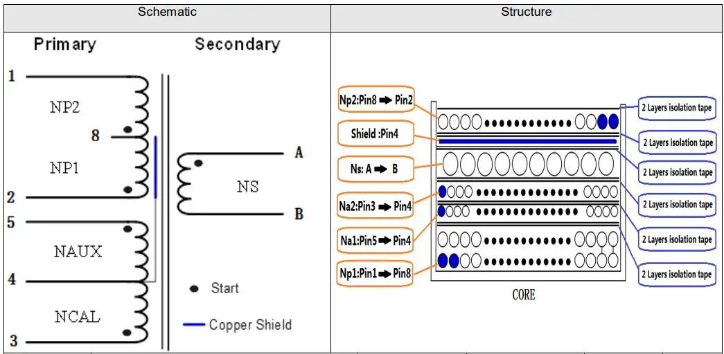
| Windings | Wire Gauge | Turns | Start Pin | End Pin | Tape | ||
| Np1 | Φ0.1 2UEW*20P | 21 | 1 | 8 | 2T | ||
| Na1 | 0.12 2UEW | 4 | 5 | 4 | 2T | ||
| Na2 | Φ0.12 2UEW*4P | 12 | 3 | 4 | 2T | ||
| Ns | Φ0.30 TEX-E*7P | 5 | F+ | F- | 2T | ||
| Shield | Φ0.14 2UEW*2P | 22 | 4 | NC | 2T | ||
| Np2 | Φ0.1 2UEW*20P | 11 | 8 | 2 | 2T | ||
| BOBBIN PIN Define:
| |||||||
| Item | Test Condition | Rating | |||||
| Primary Inductance | Pin1-2,all other windings open, measured at 100kHz / 1V | 390uH+/- 5% | |||||
| Note | Bobbin: ATQ2516 Core ATQ2516 | ||||||
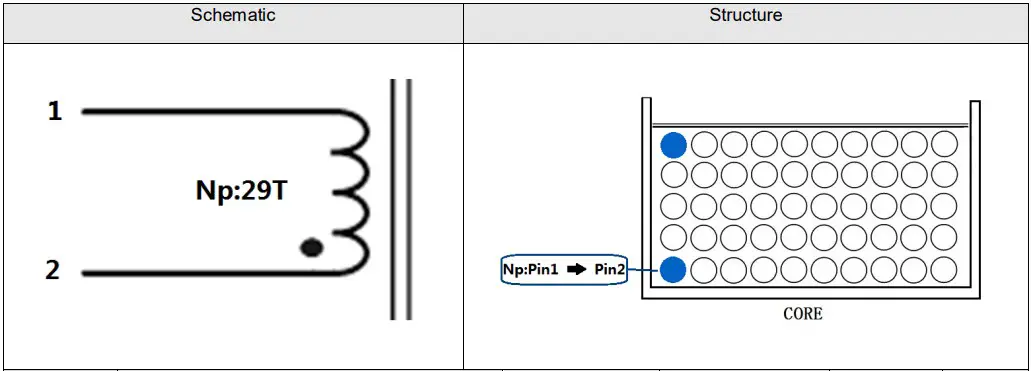
| Windings | Wire Gauge | Turns | Start Pin | End Pin | Tape | ||
| Np | Φ0.15 2UEW*20P | 29 | 1 | 2 | 2T | ||
BOBBIN PIN Define: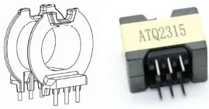 | |||||||
| Item | Test Condition | Rating | |||||
| Primary Inductance | Pin1-2,all other windings open, measured at 100kHz / 1V | 200uH+/- 5% | |||||
| Note | Bobbin: ATQ2315 Core ATQ2315 | ||||||
3.4 Schematics Description
3.4.1 AC Input Circuit & Differential Filter
The Fuse F1 protects against over-current conditions which occur when some main components fails. The L4 and L5 are common-mode chocks for the common mode noise suppression. The BD1 and BD2 are bridge rectifier which converts alternating current and voltage into direct current and voltage. The C4, C9, L1 are composed of the Pi filter for filtering the differential switching noise back to AC source.
3.4.2 AP33510 PWM Controller
AP33510, a highly integrated Quasi-Resonant Fullback (QR) controller, integrates high-voltage start-up function through HV pin and X-capacitor discharging function. It also integrates a VCC LDO circuit, which allows the LDO to regulate the wide range VCCL to an acceptable value. This makes the AP33510 an ideal candidate for wide range output voltage applications such as USB PD3.0 PPS. With embedded E-Gann drive, the AP33510 provides a safe and accurate gate signal to control switch Q4 (GaN FET) operations and achieve high-power density charger applications. At no load or light load, the AP33510 enters the burst mode to minimize standby power consumption.
3.4.3 APR349 Synchronous Rectification (SR) MOSFET Driver
As a high performance solution, the APR349 is a secondary-side SR controller to effectively reduce the secondary side rectifier power dissipation which works in both QR/DCM/CCM operation.
3.4.4 AP43771V PD 3.0 Decoder & Protection on/off N MOSFET and Interface to Power Devices
Few important pins provide critical protocol decoding and regulation functions in AP43771V:
- CC1 & CC2 (Pin 11, 10): CC1 & CC2 (Configuration Channel 1 & 2) are defined by USB Type-C spec to provide the channel communication link between power source and sink device.
- Constant Voltage (CV): The CV is implemented by sensing VFB (pin 8) and comparing with internal reference voltage to generate a CV compensation signal on the OCDRV pin (pin 5). The output voltage is controlled by firmware through CC1/CC2 channel communication with the sink device.
- Constant Current (CC): The CC is implemented by sensing the current sense resistor (RCS, 10mΩ, 1%, Low TCR) and compared with internal programmable reference voltage. The output current is controlled by firmware through CC1/CC2 channel communication with the sink device.
- Loop Compensation: R19 & C19 form the voltage loop compensation circuit, and C18 form the current loop compensation circuit.
- OCDRV (Pin5): It is the key interface link from secondary decoder (AP43771V) to primary regulation circuit (AP33510). It is connected to Opto-coupler PC1 Pin 2 (Cathode) for feedback information based on all sensed CC1 & CC2 signals for getting desired Vbus voltage & current.
- PWR_EN (Pin2) to N-MOSFET Gate: The pin is used to turn on/off N-MOSFET (Q1) to enable/disable voltage output to the Bus.
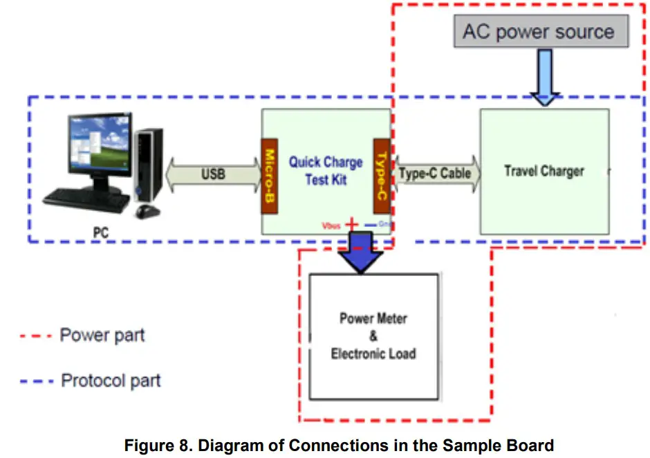
The Evaluation Board (EVB) Connections
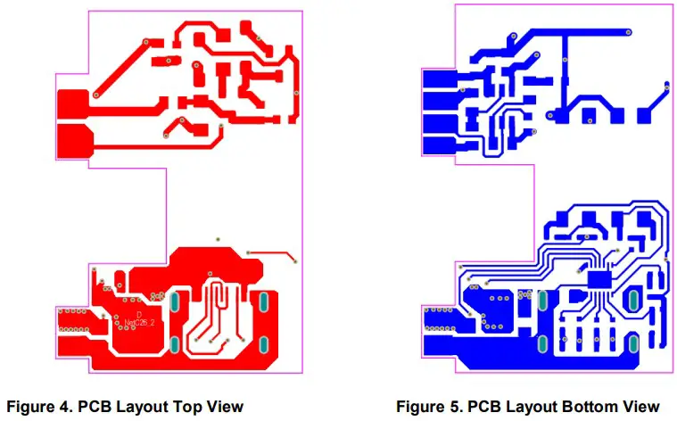
4.1 EVB PCB Layout
Main Board – 1
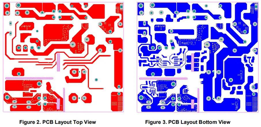
Daughter Board
4.2 Quick Start Guide before Connection
1) Before starting the 100W EVB test, the end user needs to prepare the following tool, software and manuals.
For details, please consult USBCEE sales through below link for further information.
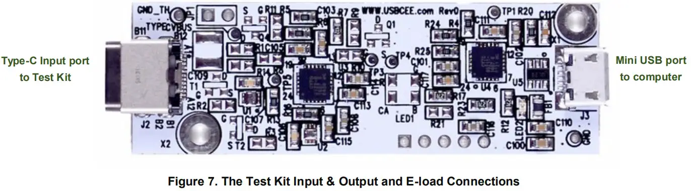
USBCEE PD3.0 Test Kit: USBCEE Power Adapter Tester. https://www.usbcee.com/product-details/4
| USBCEE PAT Tester | GUI Display | USB-A to Micro-B Cable | Type-C Cable |
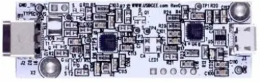 | 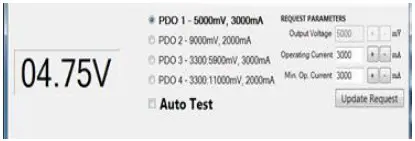 |  | 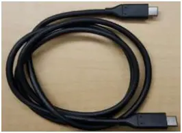 |
Figure 6. Test Kit / Test Cables
- Prepare a certified three-foot USB Type-C® cable and a Standard-A to Micro-B Cable.
- Connect the AC inputs: L & N wires of EVB to AC power supply output “L and N “wires.
- Ensure that the AC source is switched OFF or disconnected before the connection steps.
- A type-C cable for the connection between EVB’s and Type-C receptacles of test kit.
- Output of Type-C port & USB A-port are connected to E-load + & – terminals by cables.
Connection with E-Load
Testing the Evaluation Board
5.1 Input & Output Characteristics
5.1.1 Input Standby Power
| Vin(Vac) | F(Hz) | Pin(mW) |
| 90 | 60 | 21.5 |
| 115 | 60 | 23.9 |
| 230 | 50 | 45 |
| 264 | 50 | 55 |
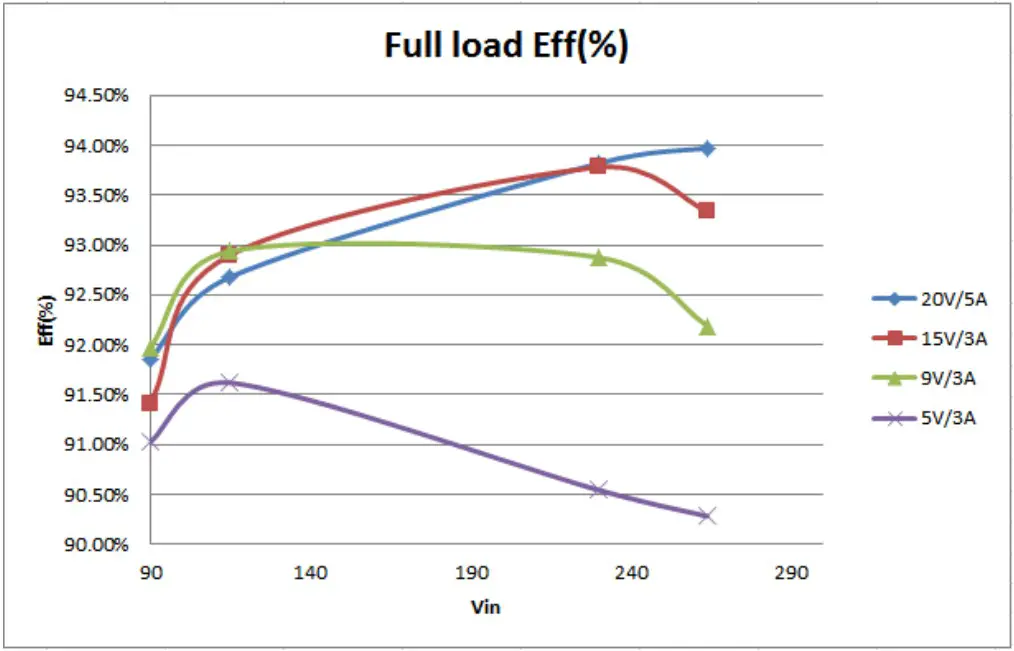
5.1.2 Multiple Output Full Load Efficiency at Different AC Line Input Voltage
| PDO Mode | Vin(Vac) | F(Hz) | Vought Board(V) | I out(A) | Pin(W) | Pout(W) | Eff(%) |
| 20V/5A | 90 | 60 | 20.38 | 4.996 | 110.85 | 101.82 | 91.85% |
| 115 | 60 | 20.38 | 4.996 | 109.86 | 101.82 | 92.68% | |
| 230 | 50 | 20.38 | 4.996 | 108.53 | 101.82 | 93.82% | |
| 264 | 50 | 20.38 | 4.996 | 108.35 | 101.82 | 93.97% | |
| 15V/3A | 90 | 60 | 15.21 | 3.002 | 49.95 | 45.66 | 91.41% |
| 115 | 60 | 15.21 | 3.002 | 49.15 | 45.66 | 92.90% | |
| 230 | 50 | 15.21 | 3.002 | 48.69 | 45.66 | 93.78% | |
| 264 | 50 | 15.21 | 3.002 | 48.92 | 45.66 | 93.34% | |
| 9V/3A | 90 | 60 | 9.17 | 3.002 | 29.93 | 27.53 | 91.98% |
| 115 | 60 | 9.17 | 3.002 | 29.62 | 27.53 | 92.94% | |
| 230 | 50 | 9.17 | 3.002 | 29.64 | 27.53 | 92.88% | |
| 264 | 50 | 9.17 | 3.002 | 29.86 | 27.53 | 92.19% | |
| 5V/3A | 90 | 60 | 5.15 | 3.003 | 16.99 | 15.47 | 91.03% |
| 115 | 60 | 5.15 | 3.003 | 16.88 | 15.47 | 91.62% | |
| 230 | 50 | 5.15 | 3.003 | 17.08 | 15.47 | 90.55% | |
| 264 | 50 | 5.15 | 3.003 | 17.13 | 15.47 | 90.28% |
Efficiency vs AC Line At Board End
5.1.3 Multiple Output Average Efficiency at Different Loading Port-C PD3.0_PDO_20V / 5V Average Efficiency
| Vin | Load % | Pin1 | Vought | I out | Pout | Effie. | Avg. Effie. |
| (Vrms) | (W) | (V) | (A) | (W) | (%) | (%)
| |
| 115 Vac | 100% | 109.86 | 20.38 | 4.996 | 101.82 | 92.68% |
92.69% |
| 75% | 82.45 | 20.29 | 3.75 | 76.09 | 92.28% | ||
| 50% | 54.58 | 20.22 | 2.51 | 50.75 | 92.99% | ||
| 25% | 27.14 | 20.15 | 1.25 | 25.19 | 92.81% | ||
| 230 Vac | 100% | 108.53 | 20.38 | 4.996 | 101.82 | 93.82% |
93.43% |
| 75% | 81.31 | 20.29 | 3.75 | 76.09 | 93.58% | ||
| 50% | 54.08 | 20.22 | 2.51 | 50.75 | 93.85% | ||
| 25% | 27.25 | 20.16 | 1.25 | 25.20 | 92.48% | ||
| 115 Vac | 100% | 16.88 | 5.15 | 3.003 | 15.47 | 91.62% | 91.88% |
| 75% | 12.51 | 5.11 | 2.258 | 11.54 | 92.23% | ||
| 50% | 8.26 | 5.06 | 1.502 | 7.60 | 92.01% | ||
| 25% | 4.14 | 5.02 | 0.756 | 3.80 | 91.67% | ||
| 230 Vac | 100% | 17.08 | 5.15 | 3.003 | 15.47 | 90.55% | 89.74% |
| 75% | 12.72 | 5.11 | 2.258 | 11.54 | 90.71% | ||
| 50% | 8.44 | 5.06 | 1.502 | 7.60 | 90.05% | ||
| 25% | 4.33 | 5.02 | 0.756 | 3.80 | 87.65% |
Port-C PD3.0_PDO_9V / 15V Average Efficiency
| Vin | Load % | Pin1 | Out | Out | Pout | Effie. | Avg. Effie. |
| (Vrms) | (W) | (V) | (A) | (W) | (%) | (%) | |
| 115n Vac | 100% | 29.62 | 9.17 | 3.002 | 27.53 | 92.94% | 92.93% |
| 75% | 22.16 | 9.13 | 2.258 | 20.62 | 93.03% | ||
| 50% | 14.66 | 9.08 | 1.502 | 13.64 | 93.03% | ||
| 25% | 7.37 | 9.04 | 0.756 | 6.83 | 92.73% | ||
| 230 Vac | 100% | 29.64 | 9.17 | 3.002 | 27.53 | 92.88% | 91.94% |
| 75% | 22.3 | 9.13 | 2.258 | 20.62 | 92.45% | ||
| 50% | 14.87 | 9.09 | 1.502 | 13.65 | 91.82% | ||
| 25% | 7.54 | 9.04 | 0.756 | 6.83 | 90.64% | ||
| 115 Vac | 100% | 49.15 | 15.21 | 3.002 | 45.66 | 92.90% | 92.94% |
| 75% | 36.71 | 15.17 | 2.258 | 34.25 | 93.31% | ||
| 50% | 24.41 | 15.13 | 1.502 | 22.73 | 93.10% | ||
| 25% | 12.33 | 15.08 | 0.756 | 11.40 | 92.46% | ||
| 230 Vac | 100% | 48.69 | 15.21 | 3.002 | 45.66 | 93.78% | 92.62% |
| 75% | 36.77 | 15.17 | 2.258 | 34.25 | 93.16% | ||
| 50% | 24.57 | 15.13 | 1.502 | 22.73 | 92.49% | ||
| 25% | 12.52 | 15.08 | 0.756 | 11.40 | 91.06% |
5.2 Key Performance Waveforms
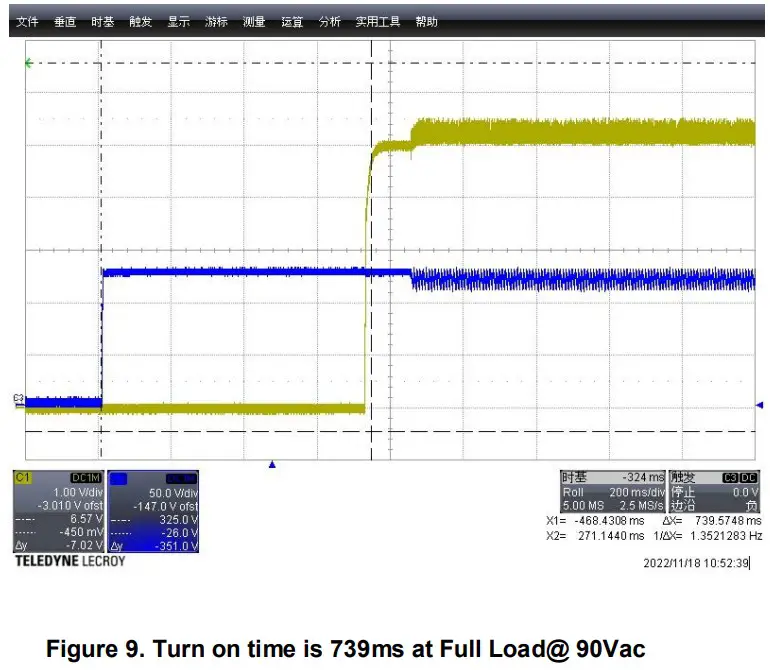
5.2.1 100W PD3.0 System Start-up Time
5.2.2 Q1 / Q2 MOSFET Voltage Stress at Full Load @264Vac
Primary side MOSFET : Q1 and Secondary side SR MOSFET- Q2
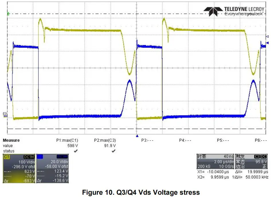
| Component | Vout | Vds | Vds_Max_Spec | Ratio of voltage stress |
| Q1 | 20V | 598V | 650V | 92% |
| Q2 | 91.9V | 100V | 91.9% |
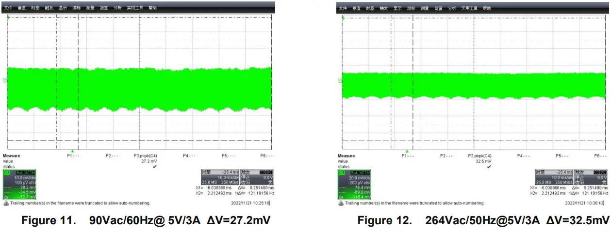
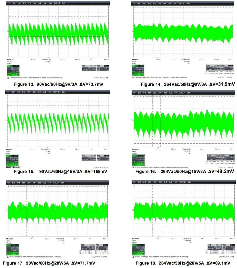
5.2.3 System Output Ripple & Noise with the Cable
Connect 47uF AL Cap and 104MLCC to the cable output unit in parallel
5.2.4 Dynamic load —-10% Load~90% Load, T=5mS, Rate=100mA/uS (PCB End)
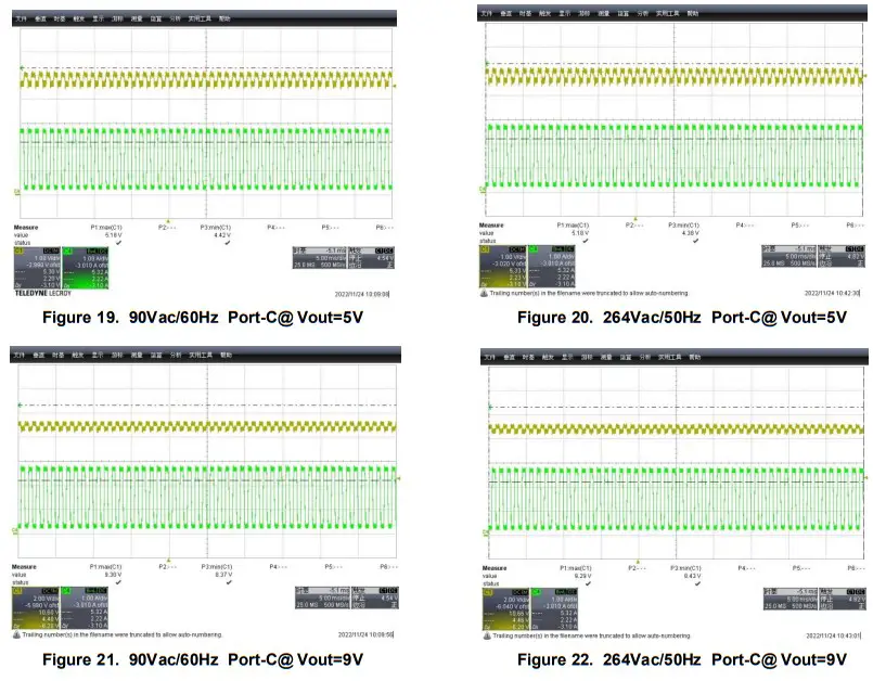
| Vo_ Undershoot(V) | Vo_ Overshoot(V) | Vo_Undershoot(V) | Vo_Overshoot(V) | ||
| Vin=90Vac@5V | 4.42 | 5.18 | Vin=90Vac@9V | 8.37 | 9.30 |
| Vin=264Vac@5V | 4.38 | 5.18 | Vin=264Vac@9V | 8.43 | 9.29 |
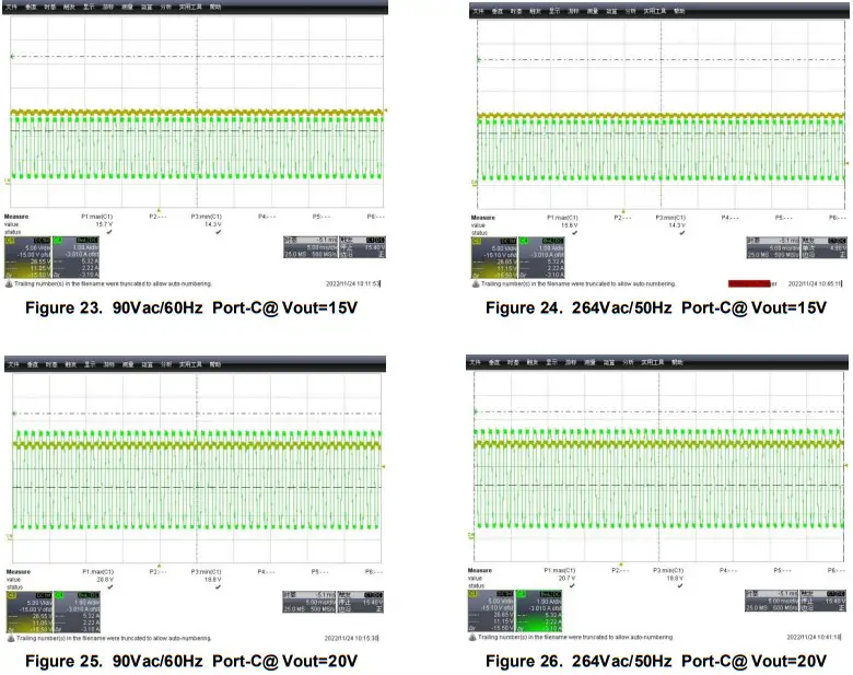
| Vo_ Undershoot(V) | Vo_ Overshoot(V) | Vo_Undershoot(V) | Vo_Overshoot(V) | ||
| Vin=90Vac@15V | 14.30 | 15.7 | Vin=90Vac@20V | 18.8 | 20.80 |
| Vin=264Vac@15V | 14.30 | 15.6 | Vin=264Vac@20V | 18.8 | 20.70 |
Output Voltage Transition Time from High to Low
5.2.7 Thermal Testing
Output Condition : 20V/3.25A
| Main Voltage | Temperature (°C) | |||||
| BD1 | Q4 | Q3 | Q2 | U1 | U4 | |
| 90Vac/60Hz | 107.6 | 118.5 | 109.3 | 97.4 | 110.0 | 89.5 |
| 264Vac/60Hz | 69.6 | 121.3 | 116.7 | 68.5 | 115.7 | 97.2 |
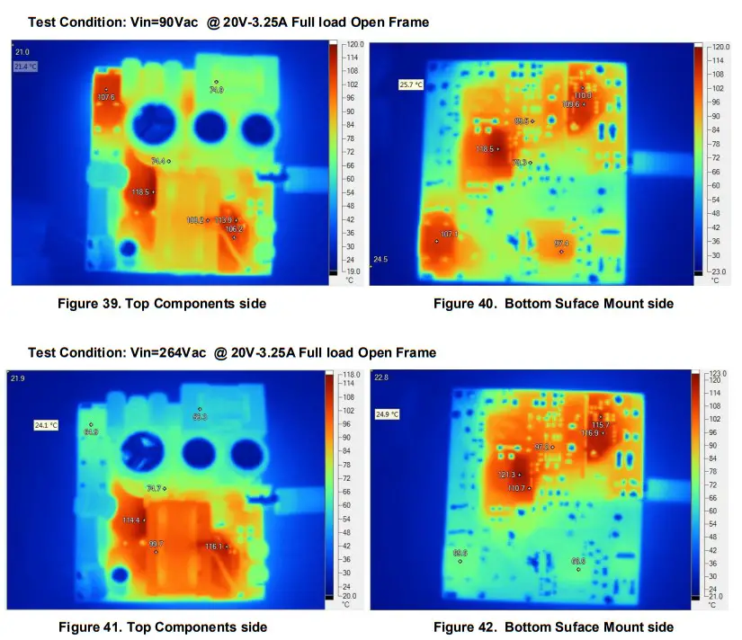
BD1: Bridge Rectifier
Q4 : Primary Side High Voltage GaN FET
Q3 : Secondary Side Sync-Rectifier
Q2 : APFC High Voltage GaN FET
U1 : AP33510, QR Controller
U4 : APR349, Sync-Rectifier Controller
Note: Component temperature can be further optimized with various system design and thermal management approaches by manufacturers.
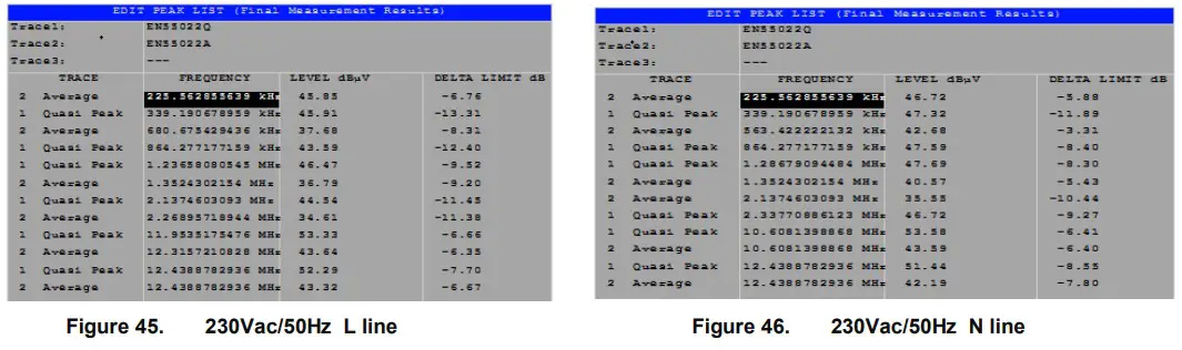
5.3 EMI (Conduction) Testing
115Vac testing results
Output Condition : 20V/5A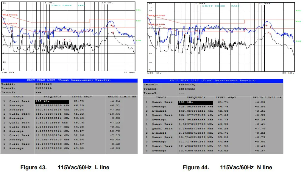
230Vac testing results
Output Condition : 20V/5A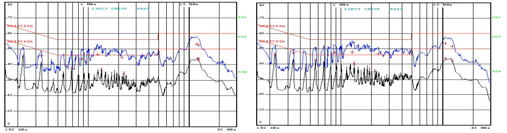
IMPORTANT NOTICE
- DIODES INCORPORATED (Diodes) AND ITS SUBSIDIARIES MAKE NO WARRANTY OF ANY KIND, EXPRESS OR IMPLIED, WITH REGARDS TO ANY INFORMATION CONTAINED IN THIS DOCUMENT, INCLUDING, BUT NOT LIMITED TO, THE IMPLIED WARRANTIES OF MERCHANTABILITY, FITNESS FOR A PARTICULAR PURPOSE OR NON-INFRINGEMENT OF THIRD PARTY INTELLECTUAL PROPERTY RIGHTS (AND THEIR EQUIVALENTS UNDER THE LAWS OF ANY JURISDICTION).
- The Information contained herein is for informational purpose only and is provided only to illustrate the operation of Diodes’ products described herein and application examples. Diodes does not assume any liability arising out of the application or use of this document or any product described herein. This document is intended for skilled and technically trained engineering customers and users who design with Diodes’ products. Diodes’ products may be used to facilitate safety-related applications; however, in all instances customers and users are responsible for (a) selecting the appropriate Diodes products for their applications, (b) evaluating the suitability of Diodes’ products for their intended applications, (c) ensuring their applications, which incorporate Diodes’ products, comply the applicable legal and r egulatory requirements as well as safety and functional-safety related standards, and (d) ensuring they design with appropriate safeguards (including testing, validation, quality control techniques, redundancy, malfunction prevention, and appropriate treatment for aging degradation) to minimize the risks associated with their applications.
- Diodes assumes no liability for any application-related information, support, assistance or feedback that may be provided by Diodes from time to time. Any customer or user of this document or products described herein wi ll assume all risks and liabilities associated with such use, and will hold Diodes and all companies whose products are represented herein or on Diodes’ websites, harmless against all damages and liabilities.
- Products described herein may be covered by one or more United States, international or foreign patents and pending patent applications. Product names and markings noted herein may also be covered by one or more United States, international or foreign trademarks and trademark applications. Diodes does not convey any license under any of its intellectual property rights or the rights of any third parties (including third parties whose products and services may be described in this document or on Diodes’ website) under this document.
- Diodes’ products are provided subject to Diodes’ Standard Terms and Conditions of Sale (https://www.diodes.com/about/company/terms-and-conditions/terms-and-conditions-of-sales/) or other applicable terms. This document does not alter or expand the applicable warranties provided by Diodes. Diodes does not warrant or accept any liability whatso ever in respect of any products purchased through unauthorized sales channel.
- Diodes’ products and technology may not be used for or incorporated into any products or systems whose manufacture, use or sa le is prohibited under any applicable laws and regulations. Should customers or users use Diodes’ products in contravention of any applicable laws or regulations, or for any unintended or unauthorized application, customers and users will (a) be solely responsible for any damages, losses or penalties arising in connection therewith or as a result thereof, and (b) indemnify and hold Diodes and its representatives and agents harmless against any and all claims, damages, expenses, and attorney fees arising out of, directly or indirectly, any claim relating to any noncompliance with the applicable laws and regulations, as well as any unintended or unauthorized application.
- While efforts have been made to ensure the information contained in this document is accurate, complete and current, it may contain technical inaccuracies, omissions and typographical errors. Diodes does not warrant that information contained in this document is error-free and Diodes is under no obligation to update or otherwise correct this information. Notwithstanding the foregoing, Diodes reserves the right to make modifications, enhancements, improvements, corrections or other changes without further notice to this document and any product described herein. This document is written in English but may be translated into multiple languages for reference. Only the English version of this document is the final and determinative format released by Diodes. Any unauthorized copying, modification, distribution, transmission, display or other use of this document (or any portion hereof) is prohibited. Diodes assumes no responsibility for any losses incurred by the customers or users or any third parties arising f rom any such unauthorized use.
- This Notice may be periodically updated with the most recent version available at https://www.diodes.com/about/company/terms-andconditions/important-notice
The Diodes logo is a registered trademark of Diodes Incorporated in the United States and other countries.
All other trademarks are the property of their respective owners.
© 2023 Diodes Incorporated. All Rights Reserved.
www.diodes.co
100W PFC+QR+GaN PD3.0 PPS Adapter EVB1
Page 28 of 28 03/9/2023
Rev 1
www.diodes.com
References
 Diodes Incorporated - Analog, Discrete, Logic, Mixed-Signal
-
Diodes Incorporated - Analog, Discrete, Logic, Mixed-Signal
-
Innoscience-Home
 YAGEO(国巨)品牌介绍_YAGEO(国巨)产品采购/价格查询-立创商城
-
muRata(村田)品牌介绍_muRata(村田)产品采购/价格查询-立创商城
-
Important Notice
-
Terms and Conditions of Sales
 Gallium Nitride (GaN) Power Devices - Transphorm
-
USBCEE


