DIODES EVB1 45W Dual Port PD3.0 Adapter
Summary
Chapter 1 provides a general description of the product and lists its key features.
General Description
The 45W Dual Port PD3.0 Adapter EVB1 is a product that provides charging capabilities for electronic devices. It is designed to be cost-effective and has a high-voltage startup with low standby power.
Key Features
The key features of the 45W Dual Port PD3.0 Adapter EVB1 are:
- CCM+Quasi-Resonant operation for NMOSFET switch Operation and
Efficiency Improvement Approaches - Cost-Effective Implementation for HPD Chargers
- High-Voltage Startup
- Low standby power
Testing the Evaluation Board
Chapter 5 provides instructions on how to test the evaluation board.
Input & Output Characteristics
This section provides information on the input standby power and multiple output average efficiency at different loading.
- Input Standby Power: This tests the amount of power used by the adapter when it is not in use.
- Multiple Output Average Efficiency at Different Loading: This tests the efficiency of the adapter at different loads.
Key Performance Waveforms
This section provides information on the performance waveforms of the product.
- 45W PD3.0 System Start-up Time: This tests the time it takes for the adapter to start up.
EMI (Conduction) Testing
This section provides information on the EMI (conduction) testing of the product.
Product Usage Instructions
To use the 45W Dual Port PD3.0 Adapter EVB1, follow these instructions:
- Connect the adapter to a power source.
- Connect your electronic device to the adapter using a compatible cable.
- The adapter will start charging your device.
- When your device is fully charged, disconnect it from the adapter and unplug the adapter from the power source.
Note: Refer to the user manual for further instructions on testing and troubleshooting the product.
Summary
General Description
- The 45W 67CC Dual USB Type-C® Ports PD3.0 PPS Evaluation Board (EVB) is composed of four main controllers, DIODES AP3304A, DIODES APR34910, DIODESTM AP43771V and Canyon Semiconductor’s CY6572. The AP3304A is a peak-current control, multi-mode CCM+QR PWM controller, which is optimized for high performance, low standby power and is a cost-effective offline flyback converter. The APR34910 is a secondary-side combo IC combining an N-Channel MOSFET and a driver circuit designed for synchronous rectification (SR).
- The AP43771V, a PD3.0 PPS protocol controller, automatically manages the PD3.0 PPS attachment process for the attached USB Type-C-equipped Device Under Charged (DUC), as well as regulates the feedback information of the charger to fulfill voltage and current requirements from DUC. The CY6572 is a synchronous buck controller. By communication between two separate channel AP43771V, two ports can realize plug in/out detection, dynamic Vbus adjustment to get best system efficiency, automatic power sharing once two ports both insert etc. By adopting the cost-effectiveness of NMOS FETs, the 45W 67CC EVB exemplifies HPD charger design with system BOM optimization to meet the market trend.
Key Features
System Key Features
- CCM+Quasi-Resonant operation for NMOSFET switch Operation and Efficiency Improvement Approaches
- Cost-Effective Implementation for HPD Chargers
- High-Voltage Startup low standby power (<20mW)
- Meets DOE VI and COC Tier 2 Efficiency Requirement
- USB Type-C® Port – Supports the Maximum Output of 45W PD3.0 PPS (3.3V to 21V@20mV/step, 50mA/step)
- SSR Topology Implementation with an Opto-coupler for Accurate Step Voltage / Current Control
- Low overall system BOM cost
AP3304A Key Features
- Operate CCM at low line and QR at high line
- QR Flyback Topology with Valley-on
- Wide VCC range(60V) to Guarantee Wide Range Output Voltage
- Soft Start During Startup Process
- Frequency Fold Back for High Average Efficiency
- Secondary Winding Short Protection with FOCP
- Frequency Dithering for Reducing EMI
- Useful Pin fault protection:
- SENSE Pin Floating Protection/
- FB/Opto-Coupler Open/Short Protection
- Comprehensive System Protection Feature: VOVP/OLP/BNO/SOVP/SUVP
- Mini Size Package of SOT26 (Type A1)
APR34910 Key Features
- SR Works with CCM / DCM / QR operation modes
- Integrate 100V, 9mOhm SR MOS
- Eliminate Resonant Ringing Interference
- Fewest External Components used
- SO-8 package
AP43771V Key Feature
- Supports USB PD Rev 3.0 V1.2
- USB-IF PD3.0/PPS Certified TID 4312
- Qualcomm® QC5 Certified: QC20201127203
- MTP for System Configuration
- OTP for Main Firmware
- Operating Voltage Range: 3.3V to 21V
- Built-In Regulator for CV and CC Control
- Programmable OVP/UVP/OCP/OTP
- Support Power Saving Mode
- External N -MOSFET Control for VBUS Power Delivery
- Support e-Marker Cable Detection
- QFN-14 and QFN-24
CY6572 Key Feature
- Wide Input Voltage from 4.5V to 40V
- Adjustable Switching Frequency to get high Efficiency
- High Duty-Cycle Up to 99%
- CC/CV Control
- Auto Recovery after Faults
- System Protection Feature
- Thermal Enhanced TSSOP-14 Package
Applications
- Quick Charger with full power range of PD3.0 PPS
Main Power Specifications
| Parameter | Value |
| Input Voltage | 90VAC to 264VAC |
| Input standby power | < 200mW |
| Master port/Slave port (Vo / Io) | PDO: 5V/3A, 9V/3A, 15V/3A, 20V/2.25A, |
| APDO: 3.3 to 11V/4.05A; 3.3V to 16V/3A: 3.3V to 21V/2.25A | |
| Voltage Step | PPS 20mV step voltage, 3.3V-21V |
| Efficiency | Comply with DoE 6 |
| Total Output Power | 45W |
| Protections | OCP, OVP, UVP, OLP, OTP, SCP |
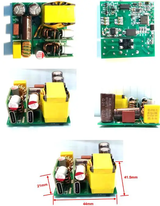
| Dimensions | PCB: 44 * 41.5 * 21 mm3, 1.732” * 1.634” * 0.827” inch3 Case: 49 * 49 * 28 mm3, 67CC, 4.1 CI |
| Power Density Index | 0.67 W/CC; 10.98 W/CI |
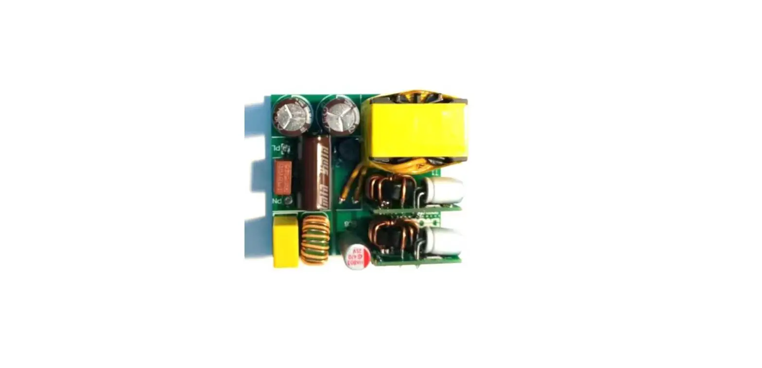
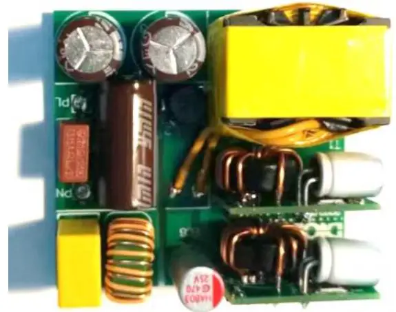
Evaluation Board Pictures
Power Supply Specification
Specification and Test Results
| Parameter | Value | Test Summary |
| Input Voltage / Frequency | 90VAC to 264VAC / 50Hz or 60Hz | Test Condition |
| Input Current | <2ARMS | PASS |
| Standby Power | < 300mW, load disconnected | PASS, 191mW@230VAC/50Hz |
| C_#1: 20V/2.25A + C_#2: No load Average Efficiency | DoE VI Efficiency >87.4% | PASS, 91.1%@115VAC/60Hz 91.46%@230VAC/50Hz |
| C_#1: 20V/2.25A + C_#2: No load (10% Load) | PASS, 84.78%@115VAC/60Hz 83.44%@230VAC/50Hz | |
| C_#1:15V/3A + C_#2: No Load Average Efficiency | DoE VI Efficiency >87.3% | PASS, 90.95%@115VAC/60Hz 90.92@230VAC/50Hz |
| C_#1:15V/3A + C_#2: No Load (10% Load) | PASS, 88.15%@115VAC/60Hz 85.68@230VAC/50Hz | |
| C_#1:15V/1.67A + C_#2: 9V/2.2A Average Efficiency | DoE VI Efficiency >87.4% | PASS, 88.74@115VAC/60Hz 88.70@230VAC/50Hz |
| C_#1:15V/1.67A + C_#2: 9V/2.2A Efficiency (10% Load) | PASS, 82.37%@115VAC/60Hz 80.1@230VAC/50Hz | |
| Output Voltage Regulation Tolerance | +/- 5% | PASS |
| 16V PPS | 3.3V – 16V +/- 5%, 0~3A +/-150mA | PASS |
| 21V PPS | 3.3V – 21V +/- 5%, 0~2.25A +/-150mA | PASS |
| Conducted EMI | >6dB Margin; according to EN55032 Class B | PASS |
Compliance
| Parameter | Test conditions | Transition time | standard | Test Summary |
|
Output Voltage Transition time | 5V to 9V | 57.2ms |
<275ms | Pass |
| 9V to 15V | 96.7ms | Pass | ||
| 15V to 20V | 74.4ms | Pass | ||
| 20V to 15V | 70.6ms | Pass | ||
| 15V to 9V | 84.9ms | Pass | ||
| 9V to 5V | 57.7ms | Pass | ||
| 20V to 5V | 108.4ms | Pass | ||
| Pass | ||||
| Output Connector | USB Type-C *2- | |||
| Temperature | Rise time @ 90Vac , Full Load; Fall time @ 264Vac , No Load; | |||
| Dimensions (W /D/ H) | L49mm x49mm x 28mm (with foldable AC pin) | |||
Schematic
Board Schematic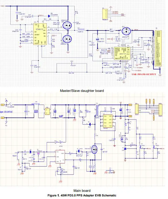
Bill of Material (BOM)
Mainboard BOM
| Description | Sign | Footprint | Quantity |
| 2.2UF/50V | C1, C2 | 0805C | 2 |
| 1nF/500V | C3 | 0805C | 1 |
| 1NF/16V | C4 | 0603C | 1 |
| 100pF 16V | C5 | 0603C | 1 |
| 2.2UF/25V | C6 | 0805C | 1 |
| 15pF 1KV | C7 | 1206C | 1 |
| NC | C8 | 0603C | 1 |
| 3.3uF/16V | C9 | 0603C | 1 |
| 1nF/250V | C20 | 0805C | 1 |
| 3.3nF/25V | C22 | 0603C | 1 |
| 1U/50V | C23 | 0805C | 1 |
| 10NF/50V | C24 | 0603C | 1 |
| 1M | R1, R1A | 1206R | 2 |
| 2.2R | R2 | 0805R | 1 |
| 180K 1% | R3 | 0603R | 1 |
| 15K 1% | R4 | 0603R | 1 |
| 30R | R5 | 1206R | 1 |
| 300K | R6 | 1206R | 1 |
| 5.1R | R7 | 0603R | 1 |
| 47R | R8 | 0603R | 1 |
| 1k | R9 | 0603R | 1 |
| 20K | R10 | 0603R | 1 |
| 10R | R20 | 1206R | 1 |
| 5.1K | R22 | 0603R | 1 |
| 4.7K | R23 | 0603R | 1 |
| 300R | R24 | 0603R | 1 |
| 91K | R25 | 0402R | 1 |
| 51K | R26 | 0402R | 1 |
| 47K | R27 | 0402R | 1 |
| 100K | R28, R30 | 0402R | 2 |
| 22K | R29 | 0402R | 1 |
| 0.75R | RS1 | 1206R | 1 |
| 0.68R | RS2, RS3 | 1206R | 2 |
| 10mH T16x12x8 | CM1 | LF10*5.3 | 1 |
| 0.22uF/275V | CX1 | CAP_X04A(10_6_7.5) | 1 |
| 1nF/400V | CY1 | CY-SMD | 1 |
| FR107 | D3 | SOD-123 | 1 |
| FR207 | D4 | SMA | 1 |
| 1N4148 | D5 | SOD-323-T | 1 |
| 4A 800V | DB1 | BRID | 1 |
| 15UF/400V | EC1 | CAP-DIP(16-8-3.5A) | 1 |
| 22UF/400V | EC2, EC3 | CAP-AI (10_5) | 2 |
| 560UF/25V | EC6 | EC6.0 | 1 |
| T3.15A/250V | F1 | FUSE4*8 | 1 |
| 4.7UH | L1 | 1206R | 1 |
| 10uH | L2 | INDUCTOR SMD | 1 |
| WMO26N65C4 | Q1 | TO-252 | 1 |
| DMZ0615E | Q2 | SOT-23 | 1 |
| 2N7002 | Q3, Q4 | SOT-23 | 2 |
| PQ2016 | T1 | PQ20 | 1 |
| AP3304A | U1 | SOT23-6 | 1 |
| OR1009 | U2 | PC-SMD | 1 |
| APR34910 | U3 | SO-8 | 1 |
| TL431 | U4 | SOT-23-431 | 1 |
Master/Slave daughter board BOM
| Comment | Designator | Footprint | Quantity |
| 220pF/50V | C16, C17, C18, C19 | C-0402 | 4 |
| 100nF/50V | C24 | 0603C | 1 |
| 10 nF/25V | C25,C49 | 0402R | 2 |
| 1nF/50V | C26 | C-0603 | 1 |
| 10nF/16V | C27 | 0402R | 1 |
| 100nF/16V | C28 | C-0402 | 1 |
| 4.7uF/10V | C29, C47 | C-0603 | 2 |
| 5.6nF/25V | C30 | 0402R | 1 |
| 680pF/25V | C58 | 0402R | 1 |
| 470R | R34 | 0402R | 1 |
| 2.2uF/50V | C45 | 0805C | 1 |
| 100nF/16V | C46 | 0402R | 1 |
| 0.1uF/16V | C48 | 0402R | 1 |
| 0.1uF/50V | C56 | C-0603 | 1 |
| 47n | C31 | 0402R | 1 |
| 1N4148WS | D6 | SOD-323 | 1 |
| 220UF/25V | EC11 | EC5.5MM – 1 | 1 |
| TYPE-C | J1 | USBC2 | 1 |
| 22UH/5A | L3 | L5 | 1 |
| AGM306A | Q11, Q12, Q13 | DFN3*3 | 3 |
| 200K | R26 | 0402R | 1 |
| 10mR | R27 | 1206R | 1 |
| 4.7K | R28, R29 | 0402R | 2 |
| 0R | R30 | 0402R | 1 |
| 15K | R31, R35 | 0402R | 2 |
| 4.7R | R32 | 0603R | 1 |
| NC | R33 | 0402R | 1 |
| 3K | R36 | 0402R | 1 |
| 10R | R52 | 0402R | 1 |
| 13K | R53 | 0402R | 1 |
| 1.5K | R54 | 0402R | 1 |
| 100K | R60 | 0402R | 1 |
| 5.1R | R70 | 0402R | 1 |
| AP43771V | U1 | QFN_24_CY2311 | 1 |
| CY6572 | U5 | TSSOP-15 | 1 |
Transformer Design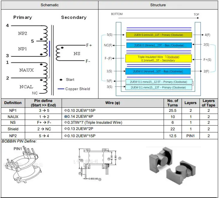
| Item | Test Condition | Rating |
| Primary Inductance | Pin 1-2, all other windings open, measured at 20kHz / 1V | 420uH+/- 5% |
| Note | Bobbin/ Core: PQ2016 (Ae=62mm²) |
Schematics Description
AC Input Circuit & Differential Filter
The Fuse F1 protects against over-current conditions which occur when some main components fails. The CM1 are common mode chocks for the common mode noise suppression. The DB is a bridge rectifier which converts alternating current and voltage into direct current and voltage. The EC1, L2, EC2, EC3 are composed of the Pi filter for filtering the differential switching noise back to AC source.
AP3304A PWM Controller
- The AP3304A is a peak-current control, multi-mode CCM+QR PWM controller which is optimized for high performance, and cost effective offline flyback converters. The AP3304A provides Mini Size Package of SOT23-6 and achieve high-power density charger applications. At no load or light load, the AP3304A enters the burst mode to minimize standby power consumption.
APR34910 Synchronous Rectification (SR) Switcher
- As a high-performance solution, The APR34910 is a secondary-side combo IC combining an N-channel MOSFET and a driver circuit designed for synchronous rectification (SR). The APR34910 effectively reduces the secondary side rectifier power dissipation which works in
QR/DCM/CCM operation.
AP43771V PD 3.0 Decoder Interface to CY6572 Sync Buck and Power Devices
Few important pins provide critical protocol decoding and regulation functions in AP43771V:
- CC1 & CC2 (Pin 11, 10): CC1 & CC2 (Configuration Channel 1 & 2) are defined by USB Type-C spec to provide the channel communication link between power source and sink device.
- Constant Voltage (CV): The CV is implemented by sensing VFB (pin 8) and comparing with internal reference voltage to generate a CV compensation signal on the OCDRV pin (pin 5). The output voltage is controlled by firmware through CC1/CC2 channel communication with the sink device.
- Constant Current (CC): The CC is implemented by sensing the current sense resistor (RCS, 10mΩ, 1%, Low TCR) and compared with internal programmable reference voltage. The output current is controlled by firmware through CC1/CC2 channel communication with the sink device.
- OCDRV (Pin5) to CY6572 COMP (Pin 4): It is the key interface link from CC/CV loop on AP43771V to Sync Buck COMP Pin (COMP) to realize Output CC/CV control. OCDRV is connected to CY6572 Pin 4(COMP) for feedback desired information based on all sensed Vbus, Current sense and CC1 & CC2 signals for getting desired Vbus voltage and current.
- PWR_EN (Pin2) to N-MOSFET Gate: The pin is used to turn on/off N-MOSFET (Q9) to enable/disable voltage output to the Vbus.
The interface between Master and Slave Board
Master and Slave boards build interface via I2C communication. AP43771V SDA & SDL (Pin 16, 17) are defined by I2C spec to provide the channel communication link between Master and Slave, such as plug in/out, power sharing info. etc.
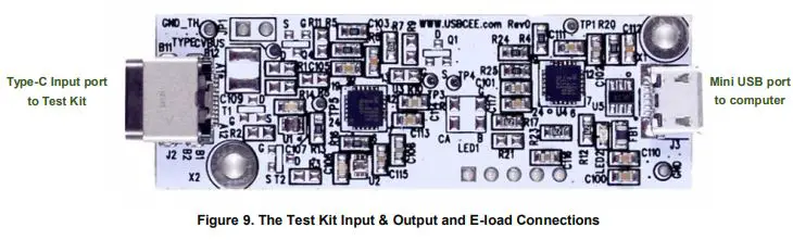
The Evaluation Board (EVB) Connections
EVB PCB Layout
Main Board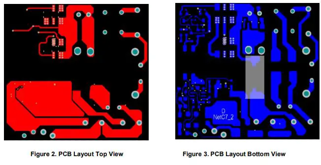
Master/Slave Daughter Board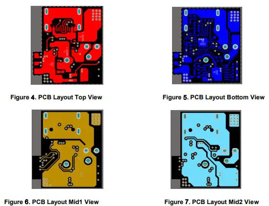
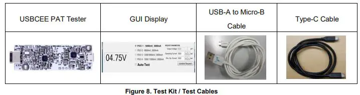
Quick Start Guide Before Connection
- Before starting the 45W EVB test, the end user needs to prepare the following tool, software and manuals. For details, please consult USBCEE sales through the below link for further information.
- USBCEE PD3.0 Test Kit: USBCEE Power Adapter Tester. https://www.usbcee.com/product-details/4

- USBCEE PD3.0 Test Kit: USBCEE Power Adapter Tester. https://www.usbcee.com/product-details/4
- Prepare a certified three-foot Type-C cable and a Standard-A to Micro-B Cable.
- Connect the AC inputs: L & N wires of EVB to AC power supply output “L and N “wires.
- Ensure that the AC source is switched OFF or disconnected before the connection steps.
- A Type-C cable for the connection between EVBs and Type-C receptacles of the test kit.
- The output of the Type-C port & USB A-port is connected to E-load + & – terminals by cables.

Connection with E-Load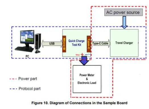
Testing the Evaluation Board
Input & Output Characteristics Input Standby Power
| Vin(Vac) | F(Hz) | Pin(mW) |
| 115 | 60 | 147 |
| 230 | 50 | 191 |
Average Efficiency at Different Loading
Smart Power Sharing Strategy:
| C1 | C2 | |
| Single Port Plug in | 45W | X |
| X | 45W | |
| Dual Port Plug in | 15W (First Plug in, Request 5V below Voltage) | 30W (Second Plug in) |
| 30W (First Plug in, Request 15V,20V Voltage) | 15W (Second Plug in, Request 5V below Voltage) | |
| 18W (First Plug in, Request 9V, 9V PPS) | 27W (Second Plug in, Request 15V, 20V, 15VPPS, 20VPPS) | |
| 27W (First Plug in, Request 15V, 20V, 15VPPS, 20VPPS) | 18W (Second Plug in, Request 9V, 9VPPS) | |
| Source cap | ||
| 45W (Power limit) | 5V/3A, 9V/3A, 15V/3A, 20V/2.25A, 3.3-11V/4.05A, 3.3-16V/3A, 3.3-21V/2.25A | |
| 30W (Power limit) | 5V/3A, 9V/3A, 15V/2A, 20V/1.5A, 3.3-11V/3A | |
| 27W (Power limit) | 5V/3A, 9V/3A, 15V/1.8A, 20V/1.35A, 3.3-11V/3A | |
| 18W (Power limit) | 5V/3A, 9V/2A, 15V/1.2A, 20V/0.9A, 3.3-11V/2A | |
| 15W (Power limit) | 5V/3A, 9V/1.67A, 15V/1A, 20V/0.75A, 3.3-11V/1.36A | |
Single Port Output: C_#1 or C_#2 : 20V / 2.25A
| Vin | Load % | Pin1 | Vout | About | Pout | Effi. | Avg. Effi. | DOE 6 required | |
| (Vrms) | (W) | (V) | (A) | (W) | (%) | (%) | |||
| 90 Vac | 100% | 50 | 20.361 | 2.2 | 44.7942 | 89.59% | 89.63% | 87.60% | |
|
115 Vac | 100% | 49.172 | 20.361 | 2.2 | 44.7942 | 91.10% |
90.37% |
87.60% | |
| 75% | 36.857 | 20.312 | 1.65 | 33.5148 | 90.93% | ||||
| 50% | 24.65 | 20.265 | 1.1 | 22.2915 | 90.43% | ||||
| 25% | 12.496 | 20.222 | 0.55 | 11.1221 | 89.01% | ||||
| 10% | 5.241 | 20.197 | 0.22 | 4.44334 | 84.78% | ||||
|
230 Vac | 100% | 48.99 | 20.367 | 2.2 | 44.8074 | 91.46% |
90.29% |
87.60% | |
| 75% | 36.843 | 20.323 | 1.65 | 33.53295 | 91.02% | ||||
| 50% | 24.7 | 20.275 | 1.1 | 22.3025 | 90.29% | ||||
| 25% | 12.584 | 20.227 | 0.55 | 11.12485 | 88.40% |
| 10% | 5.326 | 20.2 | 0.22 | 4.444 | 83.44% | |||
| 264 Vac | 100% | 49.09 | 20.362 | 2.2 | 44.7964 | 91.25% | 90.13% | 87.60% |
C_#1 or C_#2 : 15V / 3A
| Vin | Load % | Pin1 | Vout | Iout | Pout | Effi. | Avg. Effi. | DOE 6 required |
| (Vrms) | (W) | (V) | (A) | (W) | (%) | (%) | ||
| 90 Vac | 100% | 51.74 | 15.377 | 3 | 46.131 | 89.16% | 90.19% | 87.60% |
|
115 Vac | 100% | 50.77 | 15.367 | 3 | 46.101 | 90.80% |
90.95% |
87.60% |
| 75% | 37.68 | 15.302 | 2.25 | 34.4295 | 91.37% | |||
| 50% | 25.049 | 15.237 | 1.5 | 22.8555 | 91.24% | |||
| 25% | 12.593 | 15.177 | 0.75 | 11.38275 | 90.39% | |||
| 10% | 5.154 | 15.145 | 0.3 | 4.5435 | 88.15% | |||
|
230 Vac | 100% | 50.347 | 15.37 | 3 | 46.11 | 91.58% |
90.92% |
87.60% |
| 75% | 37.68 | 15.307 | 2.25 | 34.44075 | 91.40% | |||
| 50% | 25.124 | 15.246 | 1.5 | 22.869 | 91.02% | |||
| 25% | 12.701 | 15.182 | 0.75 | 11.3865 | 89.65% | |||
| 10% | 5.301 | 15.14 | 0.3 | 4.542 | 85.68% | |||
| 264 Vac | 100% | 50.5 | 15.364 | 3 | 46.092 | 91.27% | 90.48% | 87.60% |
Dual Port-C Output: 110Vac
| Load % | 100% | 75% | 50% | 25% | ||||||
|
AC110V 57HZ | ITEM | Voltage/Current:5V3A+5V3A | ||||||||
| PORT | USBC1 | USBC2 | USBC1 | USBC2 | USBC1 | USBC2 | USBC1 | USBC2 | Av eff | |
| CURRENT | 3.00A | 3.00A | 2.25A | 2.25A | 1.50A | 1.50A | 0.75A | 0.75A |
87.67% | |
| VOLTAGE | 5.30V | 5.32V | 5.23V | 5.24V | 5.16V | 5.16V | 5.08V | 5.09V | ||
| INPUT POWER | 36.87W | 26.88W | 17.47W | 8.66W | ||||||
| EFFICIENCE | 86.41% | 87.64% | 88.57% | 88.06% | ||||||
| ITEM | Voltage/Current:9V2A+9V3A | |||||||||
| PORT | USBC1 | USBC2 | USBC1 | USBC2 | USBC1 | USBC2 | USBC1 | USBC2 | Av eff | |
| CURRENT | 2.00A | 3.00A | 1.50A | 2.25A | 1.00A | 1.50A | 0.50A | 0.75A |
89.01% | |
| VOLTAGE | 9.21V | 9.31V | 9.16V | 9.23V | 9.11V | 9.16V | 9.06V | 9.08V | ||
| INPUT POWER | 52.56W | 38.72W | 25.40W | 12.77W | ||||||
| EFFICIENCE | 88.17% | 89.12% | 89.93% | 88.80% | ||||||
| ITEM | Voltage/Current:15V1.8A+9V2A | |||||||||
| PORT | USBC1 | USBC2 | USBC1 | USBC2 | USBC1 | USBC2 | USBC1 | USBC2 | Av eff | |
| CURRENT | 1.80A | 2.00A | 1.35A | 1.50A | 0.90A | 1.00A | 0.45A | 0.50A |
89.05% | |
| VOLTAGE | 15.23V | 9.21V | 15.18V | 9.16V | 15.14V | 9.10V | 15.10V | 9.05V | ||
| INPUT POWER | 51.35W | 38.10W | 25.41W | 12.91W | ||||||
| EFFICIENCE | 89.26% | 89.83% | 89.44% | 87.68% | ||||||
| ITEM | Voltage/Current:15V2A+5V3A | |||||||||
| PORT | USBC1 | USBC2 | USBC1 | USBC2 | USBC1 | USBC2 | USBC1 | USBC2 | Av eff | |
| CURRENT | 2.00A | 3.00A | 1.500A | 2.250A | 1.000A | 1.500A | 0.500A | 0.750A | 88.74% | |
| VOLTAGE | 15.26V | 5.32V | 15.20V | 5.24V | 15.15V | 5.16V | 15.10V | 5.09V | ||
| INPUT POWER | 52.38W | 38.56W | 25.73W | 12.98W | ||||||
| EFFICIENCY | 88.74% | 89.70% | 88.96% | 87.58% | ||||||
| ITEM | Voltage/Current: PPS 3.3V3.3A+3.3V3.3A | |||||||||
| PORT | USBC1 | USBC2 | USBC1 | USBC2 | USBC1 | USBC2 | USBC1 | USBC2 | Av eff | |
| CURRENT | 3.30A | 3.30A | 2.475A | 2.475A | 1.650A | 1.650A | 0.825A | 0.825A |
85.36% | |
| VOLTAGE | 3.290V | 3.300V | 3.290V | 3.300V | 3.297V | 3.306V | 3.301V | 3.307V | ||
| INPUT POWER | 25.79W | 19.41W | 12.69W | 6.25W | ||||||
| EFFICIENCE | 84.32% | 84.03% | 85.85% | 87.23% | ||||||
Dual Port-C Output: 230Vac
|
AC230V 50HZ | Load % | 100% | 75% | 50% | 25% | |||||
| ITEM | Voltage/Current:5V3A+5V3A | |||||||||
| PORT | USBC1 | USBC2 | USBC1 | USBC2 | USBC1 | USBC2 | USBC1 | USBC2 | AV EFF | |
| CURRENT | 3.00A | 3.00A | 2.25A | 2.25A | 1.50A | 1.50A | 0.75A | 0.75A |
87.45% | |
| VOLTAGE | 5.31V | 5.32V | 5.23V | 5.24V | 5.16V | 5.16V | 5.08V | 5.08V | ||
| INPUT POWER | 36.85W | 26.71W | 17.57W | 8.76W | ||||||
| EFFICIENCE | 86.51% | 88.20% | 88.07% | 87.02% | ||||||
| ITEM | Voltage/Current:9V2A+9V3A | |||||||||
| PORT | USBC1 | USBC2 | USBC1 | USBC2 | USBC1 | USBC2 | USBC1 | USBC2 | AV EFF | |
| CURRENT | 2.00A | 3.00A | 1.50A | 2.25A | 1.00A | 1.50A | 0.50A | 0.75A |
89.23% | |
| VOLTAGE | 9.21V | 9.31V | 9.16V | 9.23V | 9.11V | 9.15V | 9.06V | 9.07V | ||
| INPUT POWER | 51.88W | 38.35W | 25.54W | 12.85W | ||||||
| EFFICIENCE | 89.34% | 89.98% | 89.41% | 88.19% | ||||||
| ITEM | Voltage/Current:15V1.8A+9V2A | |||||||||
| PORT | USBC1 | USBC2 | USBC1 | USBC2 | USBC1 | USBC2 | USBC1 | USBC2 | AV EFF | |
| CURRENT | 1.80A | 2.00A | 1.35A | 1.50A | 0.90A | 1.00A | 0.45A | 0.50A |
89.30% | |
| VOLTAGE | 15.23V | 9.21V | 15.18V | 9.16V | 15.14V | 9.10V | 15.10V | 9.05V | ||
| INPUT POWER | 50.67W | 38.00W | 25.41W | 12.98W | ||||||
| EFFICIENCE | 90.46% | 90.09% | 89.44% | 87.21% | ||||||
| ITEM | Voltage/Current:15V2A+5V3A | |||||||||
| PORT | USBC1 | USBC2 | USBC1 | USBC2 | USBC1 | USBC2 | USBC1 | USBC2 | AV EFF | |
| CURRENT | 2.00A | 3.00A | 1.500A | 2.250A | 1.000A | 1.500A | 0.500A | 0.750A |
89.17% | |
| VOLTAGE | 15.25V | 5.32V | 15.20V | 5.25V | 15.15V | 5.16V | 15.10V | 5.08V | ||
| INPUT POWER | 51.56W | 38.41W | 25.74W | 12.98W | ||||||
| ITEM | 90.11% | 90.11% | 88.93% | 87.52% | ||||||
| PORT | Voltage/Current:PPS 3.3V3.3A+3.3V3.3A | |||||||||
| CURRENT | USBC1 | USBC2 | USBC1 | USBC2 | USBC1 | USBC2 | USBC1 | USBC2 | AV EFF | |
| VOLTAGE | 3.30A | 3.30A | 2.475A | 2.475A | 1.650A | 1.650A | 0.825A | 0.825A |
85.74% | |
| INPUT POWER | 3.291V | 3.300V | 3.297V | 3.306V | 3.297V | 3.308V | 3.302V | 3.309V | ||
| EFFICIENCY | 25.73W | 18.95W | 12.59W | 6.37W | ||||||
| ITEM | 84.53% | 86.24% | 86.56% | 85.62% | ||||||
Key Performance Waveforms
45W PD3.0 System Start-up Time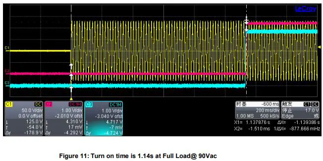
Q1 / Q2 MOSFET Voltage Stress at Full Load @264Vac
Primary side MOSFET: Q1 and Secondary side SR MOSFET- Q2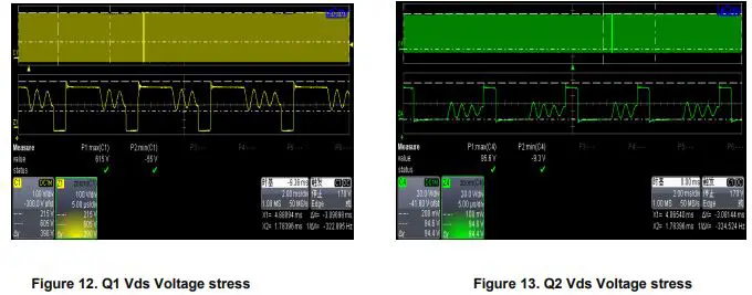
| Component | Vout | Vds | Vds_Max_Spec | Ratio of voltage stress |
| Q1 | 20V | 615V | 650V | 94.6% |
| Q2 | 95.6V | 100V | 95.6% |
System Output Ripple & Noise with the Cable
Connect 47uF AL Cap and 104MLCC to the cable output unit in parallel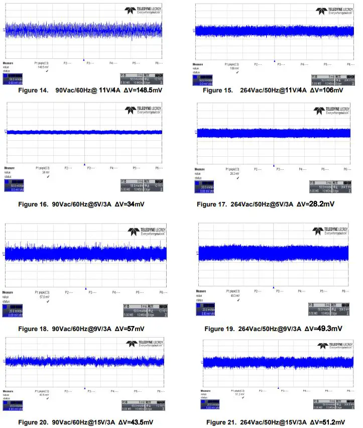
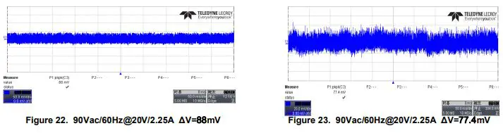
Dynamic load —-0% Load~100% Load, T=20mS, Rate=15mA/uS (PCB End)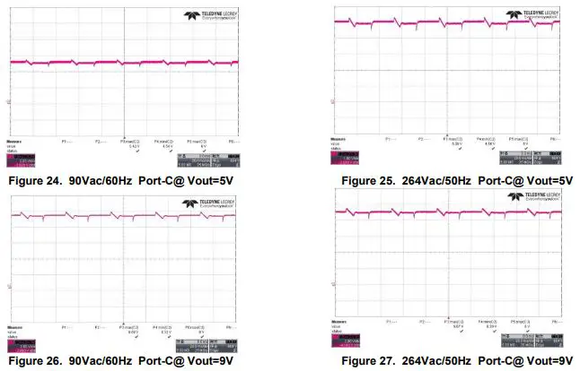
| Vo_ Undershoot(V) | Vo_ Overshoot(V) | Vo_Undershoot(V) | Vo_Overshoot(V) | ||
| Vin=90Vac@5V | 4.54 | 5.42 | Vin=90Vac@9V | 8.32 | 9.59 |
| Vin=264Vac@5V | 4.56 | 5.38 | Vin=264Vac@9V | 8.29 | 9.67 |
| Vo_ Undershoot(V) | Vo_ Overshoot(V) | Vo_Undershoot(V) | Vo_Overshoot(V) | ||
| Vin=90Vac@15V | 13.85 | 15.79 | Vin=90Vac@20V | 19.95 | 20.67 |
| Vin=264Vac@15V | 13.72 | 15.95 | Vin=264Vac@20V | 19.91 | 20.68 |
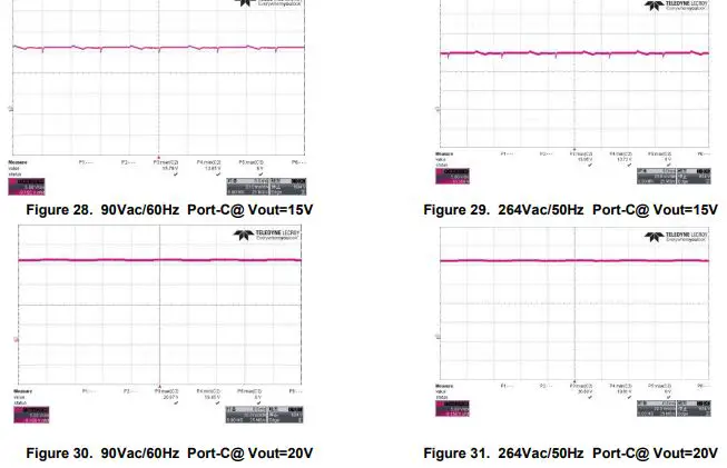
Output Voltage Transition Time from Low to High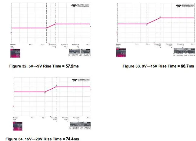
Output Voltage Transition Time from High to Low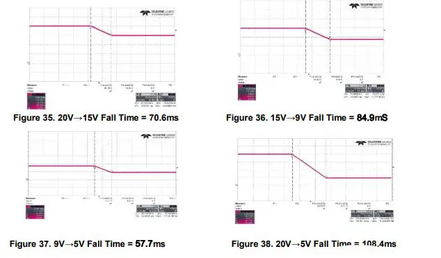
Thermal Testing
Output Condition : 1C:11V/1.64A 2C : 9V3A
| Main Voltage | Temperature (°C) | ||||||
| Ta | Q1 | T1-core | T1-wire | Q2 | L3 | DB1 | |
| 90Vac/60Hz | 25 | 101 | 82.4 | 97.6 | 111.5 | 89.4 | 104.8 |
Test Condition: Vin=90Vac @ 1C:11V/1.64A 2C : 9V3A Full load Open Frame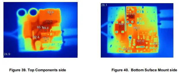
- DB1: Bridge Rectifier
- Q1: Primary Side High Voltage GaN FET T1: Transformer
- Q2: Secondary Side Sync-Rectifier
- L3: BUCK inductor
- Note: Component temperature can be further optimized with various system design and thermal management approaches by manufacturers.
EMI (Conduction) Testing 115Vac testing results
Output Condition : C1:15V/2A C2 :5V/3A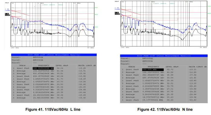
230Vac testing results
Output Condition : C1:15V/2A C2 :5V/3A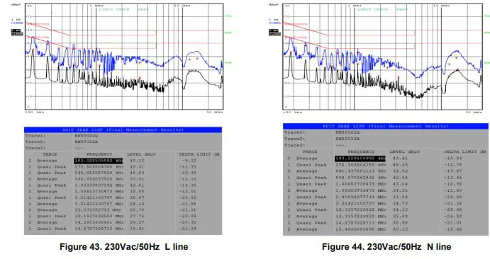
IMPORTANT NOTICE
- DIODES INCORPORATED (Diodes) AND ITS SUBSIDIARIES MAKE NO WARRANTY OF ANY KIND, EXPRESS OR IMPLIED, WITH REGARDS TO ANY INFORMATION CONTAINED IN THIS DOCUMENT, INCLUDING, BUT NOT LIMITED TO, THE IMPLIED WARRANTIES OF MERCHANTABILITY, FITNESS FOR A PARTICULAR PURPOSE OR NON-INFRINGEMENT OF THIRD PARTY INTELLECTUAL PROPERTY RIGHTS (AND THEIR EQUIVALENTS UNDER THE LAWS OF ANY JURISDICTION).
- The Information contained herein is for informational purpose only and is provided only to illustrate the operation of Diodes’ products described herein and application examples. Diodes does not assume any liability arising out of the application or use of this document or any product described herein. This document is intended for skilled and technically trained engineering customers and users who design with Diodes’ products. Diodes’ products may be used to facilitate safety-related applications; however, in all instances customers and users are responsible for (a) selecting the appropriate Diodes products for their applications, (b) evaluating the suitability of Diodes’ products for their intended applications, (c) ensuring their applications, which incorporate Diodes’ products, comply the applicable legal and r egulatory requirements as well as safety and functional-safety related standards, and (d) ensuring they design with appropriate safeguards (including testing, validation, quality control techniques, redundancy, malfunction prevention, and appropriate treatment for aging degradation) to minimize the risks associated with their applications.
- Diodes assumes no liability for any application-related information, support, assistance or feedback that may be provided by Diodes from time to time. Any customer or user of this document or products described herein will assume all risks and liabilities associated with such use, and will hold Diodes and all companies whose products are represented herein or on Diodes’ websites, harmless against all damages and liabilities.
- Products described herein may be covered by one or more United States, international or foreign patents and pending patent applications. Product names and markings noted herein may also be covered by one or more United States, international or foreign trademarks and trademark applications. Diodes does not convey any license under any of its intellectual property rights or the rights of any third parties (including third parties whose products and services may be described in this document or on Diodes’ website) under this document.
- Diodes’ products are provided subject to Diodes’ Standard Terms and Conditions of Sale (2) or other applicable terms. This document does not alter or expand the applicable warranties provided by Diodes. Diodes does not warrant or accept any liability whatso ever in respect of any products purchased through unauthorized sales channel.
- Diodes’ products and technology may not be used for or incorporated into any products or systems whose manufacture, use or sale is prohibited under any applicable laws and regulations. Should customers or users use Diodes’ products in contravention of any applicable laws or regulations, or for any unintended or unauthorized application, customers and users will (a) be solely responsible for any damages, losses or penalties arising in connection therewith or as a result thereof, and (b) indemnify and hold Diodes and its representatives a nd agents harmless against any and all claims, damages, expenses, and attorney fees arising out of, directly or indirectly, any claim relating to any noncompliance with the applicable laws and regulations, as well as any unintended or unauthorized application.
- While efforts have been made to ensure the information contained in this document is accurate, complete and current, it may contain technical inaccuracies, omissions and typographical errors. Diodes does not warrant that information contained in this document is error-free and Diodes is under no obligation to update or otherwise correct this information. Notwithstanding the foregoing, Diodes rese rves the right to make modifications, enhancements, improvements, corrections or other changes without further notice to this document and any product described herein. This document is written in English but may be translated into multiple languages for reference. Only the English version of this document is the final and determinative format released by Diodes.
- Any unauthorized copying, modification, distribution, transmission, display or other use of this document (or any portion thereof) is prohibited. Diodes assume no responsibility for any losses incurred by the customers or users or any third parties arising from any such unauthorized use.
- This Notice may be periodically updated with the most recent version available at https://www.diodes.com/about/company/terms-and-conditions/important-notice
- The Diodes logo is a registered trademark of Diodes Incorporated in the United States and other countries.
- All other trademarks are the property of their respective owners.
- © 2023 Diodes Incorporated. All Rights Reserved.
- www.diodes.com
- 45W Dual Port PD3.0 Adapter EVB1 Revision 1.0
- www.diodes.com
- March 2023
- © 2023 Copyright Diodes Incorporated. All Rights Reserved


