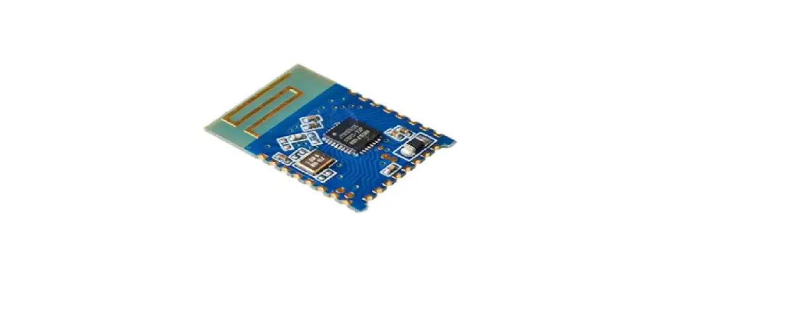
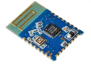
KAGA FEI WK8887 Wireless LAN and Bluetooth Module
The Bluetooth® word mark and logos are owned by the Bluetooth SIG, Inc. and any use of such marks by KAGA FEI CO., LTD. is under license.
ATTENTION: This module requires device drivers that are under Japan export control. Depending on the customer’s country and application (e.g. weapons), KAGA FEI may not be able to provide these drivers to all customers. Please contact your local KAGA FEI sales office for additional information.
To contact your local sales office and for additional product information, please visit https://www.kagafei.com/jp/eng/
Document constituent list
| Control name | Control No. | Document Page |
| General Items | KM-AG-A223020 | 1/6- 6/6 |
| Absolute maximum ratings | KM-AM-A223020 | 1/1 |
| Electrical characteristics | KM-AE-A223020 | 1/6 – 6/6 |
| Circuit schematic | KM-MC-A223020 | 1/1 |
| Outline / Appearance | KM-AD-A223020 | 1/3 – 3/3 |
| Pin Layout | KM-BA-A223020 | 1/3 – 3/3 |
| Handling Precaution | - | 1/2 – 2/2 |
Scope
This specification (“Specification”) applies to the Wireless LAN and Bluetooth ® module (“Product ”) m anufacture d by KAGA FEI C o ., L td . KAGA FEI
- Product Number: WK8887
- Function: Radio frequency transceiver Module. (IEEE802.11ac/a/b/g/n and Bluetooth®4.2 standard)
- Application: Tablets, Home audio/Video systems, Mobile routers, Handy Terminal, Game, Audio-visual equipment, Digital home electrical appliance, Mobile printer.
- This product conforms to RoHS Directive.
- Outline: 56pin leadless chip carrier.
- Marking: Part number and Lot number.
- Features:
- IEEE802.11ac/a/b/g/n and Bluetooth®4.2 standard
- Interface: SDIO3.0, PCM
- Embedded MPU for reducing loads on host processor
- Security: TKIP, WEP, AES, CCMP, CMAC, WAPI, WPA/WPA2(64bit/128bit)
- Packing: Packaging method: Reel
Packaging unit: TBD pieces/Reel
Package Material: PPE/ PET/AL/NY/PE - Mount: SMD Type
- Note
- This Product is not designed to be radiation-resistant. Please do not expose Product to radiation.
- The operating conditions of this Product are as shown in this Specification. KAGA FEI shall not be liable for any failure and/or abnormality caused by using this Product beyond its specified operating conditions.
- The Product mentioned in this Specification is manufactured for use in consumer products. Before using this Product in any special equipment (e.g. medical, space, aircraft, disaster prevention) where higher safety and reliability are required, the applicability and suitability of this Product must be fully evaluated by the customer at its sole risk to ensure correct and safe operation of those special equipment. If this Product is used in general electronics equipment, the safety function must also be thoroughly evaluated at the customer’s sole risk, and when necessary, a protective circuit shall be added during the design stage.
- Even though KAGA FEI sufficiently inspects and verifies the quality of the firmware incorporated in this Product (“Incorporated Software”), it is recommended that customers fully check and confirm by the start of mass production that (1) no bugs, defects or other failures are included in the Incorporated Software, (2) no bugs, defects or other failures are caused by installing this Product with the Incorporated Software into the customer’s product, (3) the Incorporated Software fully meets customer’s intended use.
- Please note that KAGA FEI is not responsible for any failure from bugs or defects in the Incorporated Software.
- Depending on the radio environment and operating conditions, communication between this Product and others devices may not be established or maintained.
- This Product operates at 2.4GHz and 5GHz unlicensed ISM band. If this Product is used around the other wireless devices that operate in same frequency band, there is a possibility that interference may occur. If interference occurs, please stop operation of the other devices, or relocate this Product, or do not use this Product around the other wireless devices.
- If this Product is incorporated into your device, please thoroughly evaluate its operation before mass production.
- Caution for Export Control
This Product may be subject to governmental approvals, consents, licenses, authorizations, declarations, filings, and registrations for export or re-export as required by Japanese Foreign Exchange and Foreign Trade Law (including related laws and regulations) and/or any other country’s applicable laws or regulations related to export control.
If this Product will be exported or re-exported, it is strongly recommended that customers check and confirm the necessary procedures to export or re-export this Product as required by applicable laws and regulations, and if necessary, customers must obtain the necessary and appropriate approvals or licenses from governmental authority at their own risk and expense.
FCC Regulatory Information
This device complies with part 15 of the FCC Rules. Operation is subject to the following two conditions: (1) This device may not cause harmful interference, and (2) this device must accept any interference received, including interference that may cause undesired operation.
- Please use the specified supply voltage in “Recommendation operating range” when installing this product. The final products must contain a power supply regulator and must ensure the applied voltage to this product is adjusted to always be within the operating voltage range.
- Please ensure and control your host product not to transmit on channels 12 and 13.
- Data transmission is inevitably initiated by software of host devices with the exception that several special packets are transmitted by the MAC. However, data transmission is terminated by end of packets in any cases. Therefore, it is RF transmitted only while packets are being transmitted. This modular transmitter automatically discontinues transmission in case of either absence of information to transmit or operational failure because RF parts will not be ON in neither cases.
- The device driver/firmware for this product is downloaded from a limited access web site provided by the device manufacturer and is implemented specifically for this product. The ID/password required to access the web site can be obtained after the conclusion of a contract with the device manufacturer.
- The antenna used for this transmitter must not be co-located or operating in conjunction with any other antenna or transmitter.
- Frequency Tolerance: 2.4GHz Band ±25 ppm, 5GHz Band ±20 ppm
- The device is designed to use the antennas l isted below. Do not modify the antenna or any other part of the module. Any modifications will invalidate the modular certifications and require new approvals for the host system.
Model No. Antenna Type Frequency Antenna Gain lmpedance AH104N2450D1 Monopole 2402 – 2480 MHz 2.1 dBi 50 Ω 5180-5825 MHz 2.4 dBi - CAUTION: Changes or modifications not expressly approved by the party responsible for compliance could void t h e use’s authority to operate the equipment
To maintain compliance with FCC’s RF exposure guidelines, use only the supplied antenna. Unauthorized antenna, modification, or attachments could damage the transmitter and may violate FCC regulations.
To maintain compliance with FCC’s RF exposure guidelines, this equipment should be installed and operated with minimum distance 20cm between the radiator and your body.
This product is authorized under the following conditions in USA and Canada. Please do not use this equipment outside the approval range.
- 5180 – 5240 MHz : Master / Client device
- 5260 – 5320 MHz : Client device
- 5500 – 5700 MHz : Client device
- 5745 – 5825 MHz : Master / Client device
The following channels are available for this equipment:
For 2402 2480MHz (Bluetooth BDR/EDR, Bluetooth Low Energy)
79 channels are provided for Bluetooth BDR/EDR : 0 78ch
40 channels are provided for Bluetooth Low Energy: 0 39 ch
For 24122462MHz (IEE E 802.11b/g/n 20)
11 channels are provided for 802.11bg /n( : 1 11ch
For 24222452MHz (IEEE802.11n 40)
7 channels are provided for 802.11n(HT40) : 3 9ch
For 5180 5240MHz
4 channels are provided for 802.11a, 802.11n(HT20), 802.11ac(VHT20): 36ch, 4 4ch, 48ch
2 channels are provided for 802.11n(HT40), 8 0 2.11ac(VHT40 : 38ch, 46ch
1 channel is provided for 802.11ac(VHT80) : 42ch
For 52605320MHz
4 channels are provided for 802.11a, 802.11n(HT20), 802.11ac(VHT20) : 52ch, 56ch, 60ch, 64ch
2 channels are provided for 802.11n(HT40), 802.11ac(VHT40) : 54ch 62ch
1 channel is provided for 802.11ac(VHT80): 58ch
For 5500-5700MHz
11 channels are provided for 802.11a, 802.11n(HT20), 802.11ac(VHT20) : 100ch, 104ch, 108ch, 112ch, 116ch, 120ch, 124ch, 128ch, 132ch, 136ch, 140ch
5 channels are provided for 802.11n(HT40), 802.11ac(VHT40) : 102ch, 110ch, 118ch, 126ch, 134ch
2 channels are provided for 802.11ac(VHT80) : 106ch, 122ch
For 5745-5825MHz
5 channels are provided for 802.11a, 802.11n(HT20), 802.11ac(VHT20) : 149ch, 153ch, 157ch, 161ch, 165ch
2 channels are provided for 802.11n(HT40), 802.11ac(VHT40) : 151ch, 159ch
1 channel is provided for 802.11ac(VHT80) : 155ch
- Please label FCC ID at any location on the exterior of your product. Please indicate FCC ID by either one of the following method.
- Contains Transmitter Module FCC ID: 2A6NFWK8887
- Contains FCC ID: 2A6NFWK8887
- Please include the following statements in the user manual of the host device of this module;
FCC CAUTION
Changes or modifications not expressly approved by the party responsible for compliance could void the user’s authority to operate the equipment.
Compliance with FCC requirement 15.407(c)
Data transmission is always initiated by software, which is passed down through the MAC, through the digital and analog baseband, and finally to the RF chip. Several special packets are initiated by the MAC. These are the only ways the digital baseband portion will turn on the RF transmitter, which it then turns off at the end of the packet.
Therefore, the transmitter will be on only while one of the aforementioned packets is being transmitted. In other words, this device automatically discontinues transmission in case of either absence of information to transmit or operational failure.
Frequency Tolerance: ±25 ppm (2.4GHz)
Frequency Tolerance: ±20 ppm (5GHz)
This transmitter must not be co-located or operated in conjunction with any other antenna or transmitter.
This equipment complies with FCC radiation exposure limits set forth for an uncontrolled environment and meets the FCC radio frequency (RF) Exposure Guidelines. This equipment should be installed and operated keeping the radiator at least 20cm or more away from person’s body.
This device complies with below part 15 of the FCC Rules.
Part 15 Subpart C
Part 15 Subpart E
The modular transmitter is only FCC authorized for the specific rule parts (i.e., FCC transmitter rules) listed on the grant (FCC Part 15.247), and the host product manufacturer is responsible for compliance to any other FCC rules that apply to the host not covered by the modular transmitter grant of certification.
The final host product still requires Part 15 Subpart B compliance testing with the modular transmitter installed.
Absolute maximum ratings
| Item | Symbol | Rating | Unit | Remark | ||
| Min. | Typ. | Max. | ||||
| Supply voltage 1 | VBAT | – | 3.3 | 4.5 | V | |
| Supply voltage 2 | VDD33 | – | 3.3 | 4.0 | V | |
| Supply voltage 3 | VIO | – | 1.8 | 2.2 | V | |
| – | 2.5 | 3.0 | V | |||
| – | 3.3 | 4.0 | V | |||
| Supply voltage 4 | VIO_SD | – | 1.8 | 2.2 | V | |
| – | 3.3 | 4.0 | V | |||
| Supply voltage 5 | VIO_RF | – | 3.3 | 4.0 | V | |
Recommendation operating range
| Item | Symbol | Rating | Unit | Remark | ||
| Min. | Typ. | Max. | ||||
| Supply voltage 1 | VBAT | 2.7 | 3.3 | 4.5 | V | |
| Supply voltage 2 | VDD33 | 3.0 | 3.3 | 3.6 | V | |
| Supply voltage 3 | VIO | 1.62 | 1.8 | 1.98 | V | |
| 2.25 | 2.5 | 2.75 | V | |||
| 3.0 | 3.3 | 3.6 | V | |||
| Supply voltage 4 | VIO_SD | 1.62 | 1.8 | 1.98 | V | |
| 3.0 | 3.3 | 3.6 | V | |||
| Supply voltage 5 | VIO_RF | 3.0 | 3.3 | 3.6 | V | |
| Operation temperature range | Taopr | -30 | 25 | 85 | Degrees C | |
| Storage temperature range | Tstg | -40 | 85 | Degrees C | ||
Power consumption
The Specification applies for Topr.= 25 degrees C, Supply voltage=Typical voltage
| No. | Parameter | Condition | Symbo l | Min. | Typ. | Max. | Unit | Remark |
| 1 | Power consumption1 | Tx: 12dBm 11b, 11Mbps | Pc1 | 488 | mW | Duty=46.8% | ||
| 2 | Power consumption2 | Rx 11b, 11Mbps | Pc2 | 201 | mW | |||
| 3 | Power consumption3 | Tx: 12dBm 11g, 54Mbps | Pc3 | 297 | mW | Duty=25.4% | ||
| 4 | Power consumption4 | Rx 11g, 54Mbps | Pc4 | 211 | mW | |||
| 5 | Power consumption5 | Tx: 10dBm, 40MHz BW 11n, MCS7, 2.4GHz | Pc5 | 211 | mW | Duty=2.2% | ||
| 6 | Power consumption6 | Rx, 40MHz BW 11n, MCS7, 2.4GHz | Pc6 | 251 | mW | |||
| 7 | Power consumption7 | Tx: 12dBm 11a, 54Mbps | Pc9 | 363 | mW | Duty=25.4% | ||
| 8 | Power consumption8 | Rx 11a, 54Mbps | Pc10 | 244 | mW | |||
| 9 | Power consumption9 | Tx: 10dBm , 40MHz BW 11n, MCS7, 5GHz | Pc11 | 244 | mW | Duty=2.4% | ||
| 10 | Power consumption10 | Rx, 40MHz BW 11n, MCS7, 5GHz | Pc12 | 286 | mW | |||
| 11 | Power consumption11 | Tx: 8dBm, 80MHz BW 11ac, MCS9, 5GHz | Pc13 | 321 | mW | Duty=1.4% | ||
| 12 | Power consumption12 | Rx, 80MHz BW 11ac, MCS9, 5GHz | Pc14 | 358 | mW | |||
| 13 | Power consumption13 | Power save mode (DTIM=1,Beacon_interval =100ms) | Pc15 | 5.0 | mW | |||
| 14 | Power consumption14 | Deep Sleep | Pc16 | 1.8 | mW |
- The power consumption might fluctuate with the condition of radio communication, host performance and test circuit.
- The Typ. is a reference value. The value may change depending on the evaluation.
DC Specifications
Digital Pad Ratings (SDIO, PCM, GPIO) (VIO=1.8/ 2.5/ 3.3V)
| No. | Parameter | Condition | Symbol | Min. | Typ. | Max. | Unit | Remark |
| 1 | Input High Voltage | VIH | 0.7xVIO | VIO+0.3 | V | |||
| 2 | Input Low Voltage | VIL | -0.3 | 0.3xVIO | V | |||
| 3 | Output High Voltage | VOH | VIO-0.4 | – | V | |||
| 4 | Output Low Voltage | VOL | – | 0.4 | V |
AC Specifications
Power-on timing / External sleep clock
| Parameter | Condition | Symbol | Min | Typ | Max | Unit | Remark | |
| 1 | Valid Power/ Clock to PDn de-asserted | Tpor | 300 | ms | ||||
| 2 | Input SLP_CLK frequency | Tf | – | 32.768 | – | KHz | ||
| 3 | Input SLP_CLK high voltage | V=1.8V | VIH | 0.7*V | – | V+0.4 | V | |
| 4 | Input SLP_CLK low voltage | VIL | -0.4 | 0.3*V | V | |||
| 5 | Input SLP_CLK phase noise requirement | PN | – | -125 | – | dBc/Hz | @100KHz | |
| 6 | Input SLP_CLK slew rate limit (10-90%) | SR | – | – | 100 | ns | ||
| 7 | Input SLP_CLK duty cycle tolerance | DC | 20 | – | 80 | % | ||
| 8 | PDN down to Power off | Toff | 0 | ms |
<Power-on sequence>
PDn must remain asserted for minimum of Tpor after VBAT/VDD33/VIO/VIO_RF/VIO_SD and SLP_CLK are stable.
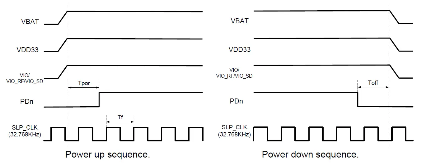
External power down(PDn)
| Parameter | Condition | Symbol | Min | Typ | Max | Unit | Remark | |
| 1 | PDn pulse width | Tppw | 300 | ms |
1. PDn should be asserted while VBAT/VDD33/VIO/VIO_RF/VIO_SD are stable.

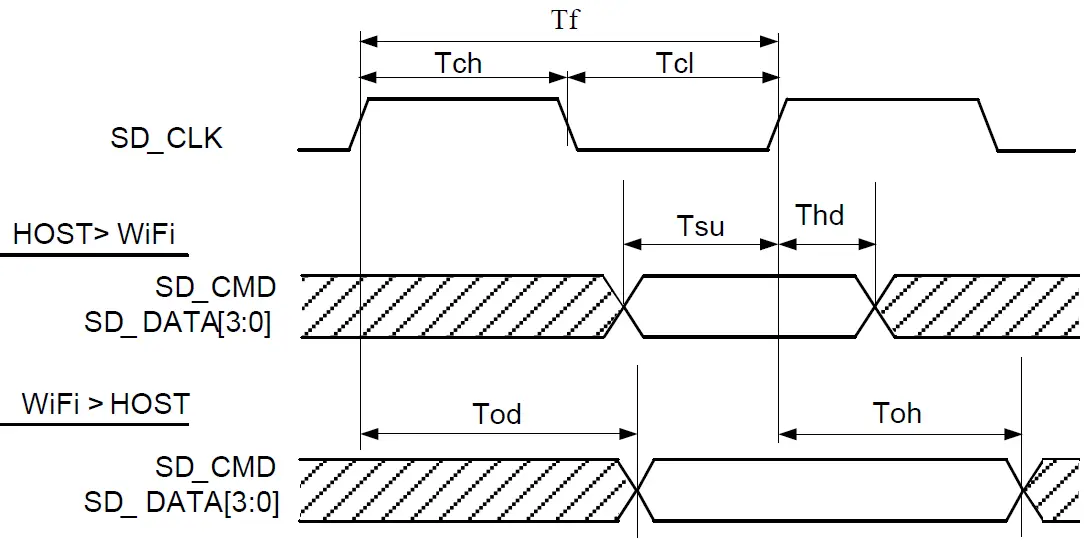
SDIO Interface Specifications
The Specification applies for Topr.= 25 degrees C , Supply voltage=Typical voltage.
| Parameter | Symbol | Condition | Min | Typ | Max | Unit | Remark | |
| 1 | Input SDIO_CLK Frequency | Tf | Normal | 0 | – | 25 | MHz | |
| High Speed | 0 | – | 50 | |||||
| 2 | Input SDIO_CLK High Time | Tch | Normal | 10 | – | – | ns | |
| High Speed | 7 | – | – | |||||
| 3 | Input SDIO_CLK Low Time | Tcl | Normal | 10 | – | – | ns | |
| High Speed | 7 | – | – | |||||
| 4 | Input SDIO_CMD, DATA[3:0] Setup time | Tsu | Normal | 5 | – | – | ns | |
| High Speed | 6 | – | – | |||||
| 5 | Input SDIO_CMD, DATA[3:0] Hold time | Thd | Normal | 5 | – | – | ns | |
| High Speed | 2 | – | – | |||||
| 6 | Output SDIO_CMD, DATA[3:0] Delay time | Tod | Normal | – | – | 14 | ns | |
| High-Speed | – | – | 14 | ns | CL<40pF (1card) | |||
| 7 | Output SDIO_CMD, DATA[3:0] Hold time | Toh | High Speed | 2.5 | – | – | ns |
Normal Mode
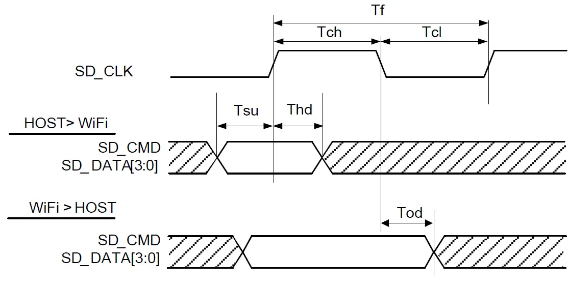
High Speed Mode
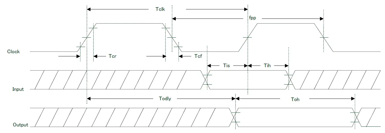
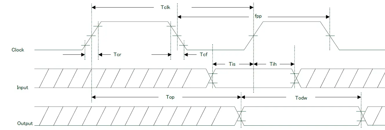
SDIO Interface Specifications
The Specification applies for Topr.= 25 degrees C , Supply voltage=Typical voltage.
| Parameter | Symbol | Condition | Min | Typ | Max | Unit | Remark | |
| 1 | Clock Frequency | fpp | SDR12/25/50 | 25 | – | 100 | MHz | |
| SDR104 | 0 | – | 150 | |||||
| 2 | Input setup time | Tis | SDR12/25/50 | 3 | – | – | ns | |
| SDR104 | 1.4 | – | – | |||||
| 3 | Input hold time | Tih | SDR12/25/50 | 0.8 | – | – | ns | |
| SDR104 | 0.8 | – | – | |||||
| 4 | Clock time | Tclk | SDR12/25/50 | 10 | – | 40 | ns | |
| SDR104 | 4.8 | – | – | |||||
| 5 | Rise time,fall time Tcr,Tcfs<2ns(max)at100MHz Ccard=10pF | Tcr,Tcf | SDR12/25/50 | – | – | 0.2*Tclk | ns | |
| SDR104 | – | – | 0.2*Tclk | |||||
| 6 | Output delay time Cl≦30pF | Todly | SDR12/25/50 | – | – | 7.5 | ns | |
| 7 | Output hold time Cl=15pF | Toh | SDR12/25/50 | 1.5 | – | – | ns | |
| 8 | Card output phase | Top | SDR104 | 0 | – | 10 | ns | |
| 9 | Output timing of variable data window | Todw | SDR104 | 2.88 | – | – | ns |
SDIO Protocol Timing Diagram-SDR12,SDR25,SDR50
SDIO Protocol Timing Daigram-SDR104
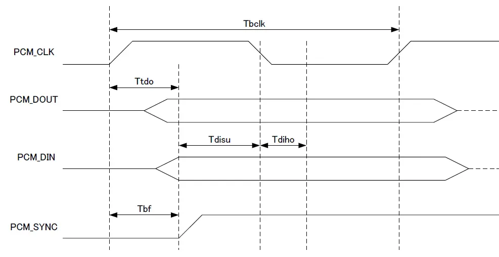
PCM Interface
The Specification applies for Topr.= 25 degrees C, Supply voltage=Typical voltage.
| No. | Parameter | Condition | Symbol | Min | Typ | Max | Unit | Remark |
| 1 | PCM_CLK Frequency | Tbclk | – | 2 / 2.048 | – | MHz | ||
| 2 | Delay time from PCM_CLK High to valid PCM_OUT | Tdo | – | – | 15 | ns | ||
| 4 | Setup time for PCM_IN valid to PCM_CLK Low | Tdisu | 20 | – | – | ns | ||
| 5 | Hold time for PCM_CLK Low to PCM_IN valid | Tdiho | 15 | – | – | ns | ||
| 6 | Delay time from PCM_CLK High to PCM_SYNC High | Tbf | – | – | 15 | ns |
Master Mode
2.4GHz Band RF Specifications
The Specification applies for Topr.= 25 degrees C, Supply voltage=Typical voltage
| No. | Parameter | Condition | Symbol | Min | Typ | Max | Unit | Remark |
|
1 |
TX Power | 11Mbps, 11b | Po2-1 | 10 | 12 | 14 |
dBm | |
| 54Mbps, 11g | Po2-2 | 10 | 12 | 14 | ||||
| MCS7, 20MHz BW, 11n | Po2-3 | 10 | 12 | 14 | ||||
| MCS7, 40MHz BW, 11n | Po2-4 | 8 | 10 | 12 | ||||
|
2 |
Rx sensitivity | 11Mbps, 11b | SEN2-1 | -87 | -76 |
dBm | ||
| 54Mbps, 11g | SEN2-2 | -73 | -65 | |||||
| MCS7, 20MHz BW, 11n | SEN2-3 | -69 | -64 | |||||
| MCS7, 40MHz BW, 11n | SEN2-4 | -66 | -61 |
5GHz Band RF Specifications
The Specification applies for Topr.= 25 degrees C, Supply voltage=Typical voltage
| No. | Parameter | Condition | Symbol | Min | Typ | Max | Unit | Remark |
|
1 |
TX Power | 54Mbps, 11a | Po5-1 | 10 | 12 | 14 |
dBm | |
| MCS7, 20MHz BW, 11n | Po5-2 | 10 | 12 | 14 | ||||
| MCS7, 40MHz BW, 11n | Po5-3 | 8 | 10 | 12 | ||||
| MCS9, 80MHz BW, 11ac | Po5-4 | 6 | 8 | 10 | ||||
|
2 |
Rx sensitivity | 54Mbps, OFDM | SEN5-1 | -71 | -65 |
dBm | ||
| MCS7,20MHzBW,OFDM | SEN5-2 | -68 | -64 | |||||
| MCS7,40MHzBW,OFDM | SEN5-3 | -65 | -61 | |||||
| MCS9,80MHzBW,OFDM | SEN5-4 | -57 | -51 |
RF Specifications (Bluetooth®)
The Specification applies for Topr.= 25 degrees C, Supply voltage =Typical voltage.
| No. | Parameter | Condition | Sym | Min | Typ | Max | Unit | Remark |
| 1 | Tx Power | Basic | Pob-2 | -6 | 0 | 2 | dBm | Class2 |
| 2 | Sensitivity | Basic | SENB | -86 | -70 | dBm |
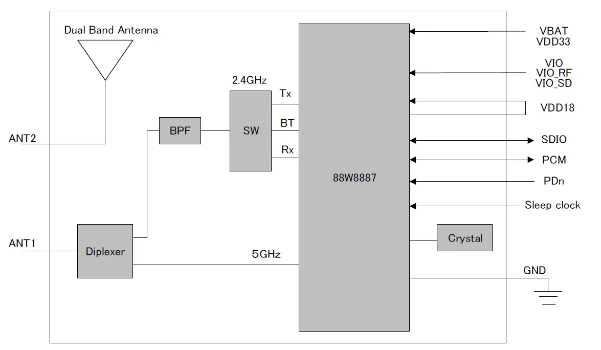
Block Diagram
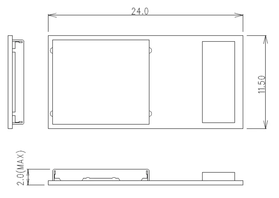
OUTLINE
Unit: mm, Tolerances unless otherwise specified: ±0.2mm
Module Pad Dimension
(TOP VIEW) Unit: mm,
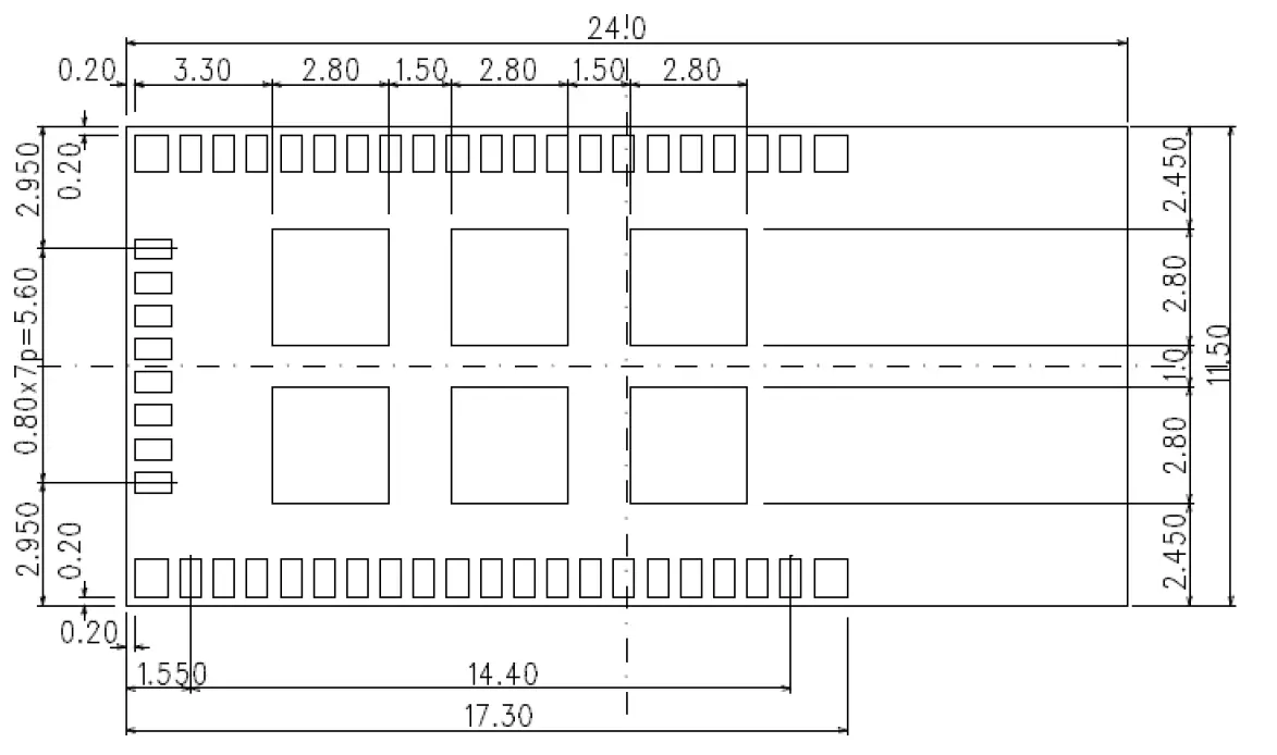
46_Singnal Pad:0.50 x 0.90
4_Corner Pad :0.80 x 0.90
6_Center Pad :□2.80
Recommended Land Pattern Dimension
Pad sizes on the motherboard should be the same size as the module pad sizes.
Recommended Metal Mask (Solder Mask) Conditions
Mask size see below. Thickness of the Metal Mask should be in the range of 0.1 mm
(TOP VIEW)
46_Singnal Pad Metal Mask Opening:0.50 x 0.90
4_Corner Pad Metal Mask Opening :0.80 x 0.90
6_Center Pad Metal Mask Opening :□2.35
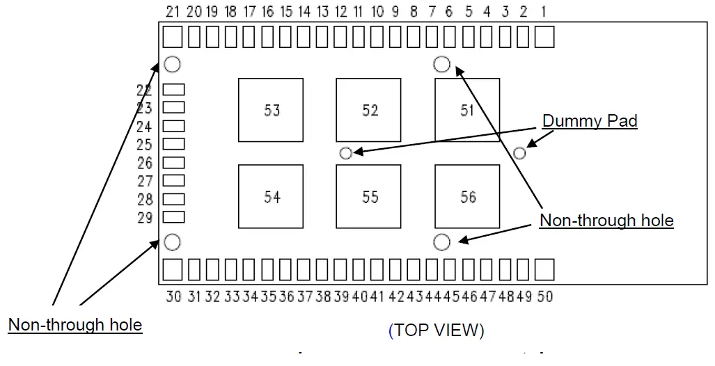
Pin Descriptions
| Terminal No. | Terminal Name | I/O | Pwr Domain | Description | Function | Internal PU |
| 1 | GND | – | GND | Ground | PWR | – |
| 2 | VIO_RF | I | VIO_RF | 3.3V Analog I/O RF Power Supply | PWR | |
| 3 | GPIO3, CON[1] | I | VIO_RF | Configuration Mode: CON[1], See Table-1 | CTRL | Enable |
| 4 | GPIO2, CON[0] | I | VIO_RF | Configuration Mode: CON[0], See Table-1 | CTRL | Enable |
| 5 | UART_RTS | O | VIO | UART_RTSN Please put out the test terminal. | UART | Enable |
| 6 | UART_CTS | I | VIO | UART_CTSN Please put out the test terminal. | UART | Enable |
| 7 | UART_SIN | I | VIO | UART_SIN Please put out the test terminal. | UART | Enable |
| 8 | UART_SOUT | O | VIO | UART_SOUT Please put out the test terminal. | UART | Enable |
| 9 | PDN | I | VIO | Power Down (no internal pull-up on this pin) (0: Full Power Down, 1: Normal Operation) | CTRL | None |
| 10 | GPIO13/BT_WAKEUP_ BT_HOST | O | VIO | Bluetooth wakeup host (Output). | CTRL | |
| 11 | GND | – | GND | Ground | PWR | – |
| 12 | VDD18 | I | VDD18 | 1.8V buck voltage output | PWR | |
| 13 | VDD33 | I | VDD33 | 3.3V Analog Power Supply | PWR | – |
| 14 | GND | – | GND | Ground | PWR | – |
| 15 | VBAT | I | VBAT | 1.1v buck/1.8v buck/3.3v LDO VBAT input | PWR | – |
| 16 | PCM_DIN/PCM_A | I | VIO | PCM Data Input Signal | PCM | Enable |
| 17 | PCM_CLK | I/O | VIO | PCM Clock Signal. (Output if PCM master. Input if PCM slave.) | PCM | Enable |
| 18 | PCM_SYNC | I/O | VIO | PCM Sync Pulse Signal. (Output if PCM master. Input if PCM slave.) | SDIO | Enable |
| 19 | PCM_DOUT/PCM_B | O | VIO | PCM Data Output Signal | PCM | Enable |
| 20 | 1.1V_INT | O | VDD11 | 1.1V buck voltage output | PWR | – |
| 21 | GND | – | GND | Ground | PWR | – |
| 22 | SD_D2 | I/O | VIO_SD | SDIO Data line Bit[2] | SDIO | Enable |
| 23 | SD_D3 | I/O | VIO_SD | SDIO Data line Bit[3] | SDIO | Enable |
| 24 | SD_CMD | I/O | VIO_SD | SDIO Command/Response | SDIO | Enable |
| 25 | GND | – | GND | Ground | PWR | – |
| 26 | SD_CLK | I | VIO_SD | SDIO Clock Input | SDIO | Enable |
| 27 | GND | – | GND | Ground | PWR | – |
| 28 | SD_D0 | I/O | VIO_SD | SDIO Data line Bit[0] | SDIO | Enable |
| 29 | SD_D1 | I/O | VIO_SD | SDIO Data line Bit[1] | SDIO | Enable |
| 30 | GND | – | GND | Ground | PWR | – |
| 31 | VIO_SD | I | VIO_SD | 1.8/3.3V Digital SDIO Power Supply. | PWR | – |
| Terminal No. | Terminal Name | I/O | Pwr Domain | Description | Function | Internal PU |
| 32 | VIO | I | VIO | 1.8/2.5/3.3V Digital Power Supply | PWR | – |
| 33 | GND | – | GND | Ground | PWR | – |
| 34 | SLP_CLK | I | VDD18 | Sleep Clock Input | CLOCK | – |
| 35 | GPIO1/WL_HOST_WAKE | O | VIO | WLAN wakeup HOST (Output) | CTRL | |
| 36 | RES | – | – | Reserved. Do not connect this pin. Leave this pin floating. | – | |
| 37 | TMS | I | VIO | JTAG Controller Select | JTAG | Enable |
| 38 | TDI | I | VIO | JTAG Test Data Input | JTAG | Enable |
| 39 | TDO | I | VIO | JTAG Test Data Output | JTAG | Enable |
| 40 | TCK | I | VIO | JTAG Test Clock Input | JTAG | Enable |
| 41 | GND | – | GND | Ground | PWR | – |
| 42 | ANT1 | I/O | – | RF I/O, should be connected to Pin 43 | RF I/O | |
| 43 | ANT2 | I/O | – | Internal antenna, should be connected to Pin 42 | Antenna | |
| 44 | GND | – | GND | Ground | PWR | – |
| 45 | GND | – | GND | Ground | PWR | – |
| 46 | RES | – | – | Reserved. Do not connect this pin. Leave this pin floating. | ||
| 47 | RES | – | – | Reserved. Do not connect this pin. Leave this pin floating. | ||
| 48 | RES | – | – | Reserved. Do not connect this pin. Leave this pin floating. | ||
| 49 | RES | – | – | Reserved. Do not connect this pin. Leave this pin floating. | ||
| 50 | GND | – | GND | Ground | PWR | – |
| 51 | GND | – | GND | Ground | PWR | – |
| 52 | GND | – | GND | Ground | PWR | – |
| 53 | GND | – | GND | Ground | PWR | – |
| 54 | GND | – | GND | Ground | PWR | – |
| 55 | GND | – | GND | Ground | PWR | – |
| 56 | GND | – | GND | Ground | PWR | – |
Table-1 HOST Interface / FW down load select
| CON[1] | CON[0] | WLAN | BT/BLE |
| 0 | 0 | 00,01 reserved | |
| 0 | 1 | ||
| 1 | 0 | SDIO | UART |
| 1 | 1 | SDIO | SDIO |
Note) The 88W8887 firmware and driver does not support UART as a Bluetooth host interface. However, please add UART test points to your design because the UART terminal may be needed during Bluetooth qualification testing.
This specification describes the required conditions for mounting the device.
Required Conditions
- Use and Storage
- If components are in the moisture barrier bag packed by KAGA FEI, store the components at < 40deg-C/90%RH.
- Keep the factory ambient conditions at < 30deg-C/60%RH .
- Store the components at < 25±5deg-C/10%RH after the bag is opened.
(This condition also applies during the manufacture process).
- Handling
Make sure all moisture barrier bags have no holes, cracks or damages. If an abnormality is found on the bag, its moisture level must be checked in accordance with 2 in (2).
Recommended Reflow Profile
- All of the surface mounting process (reflow process) must be completed within 12 months from the bag seal date.
- Immediately after opening the bag, use the humidity indicator included in the bag to make sure the humidity in the bag is less than 10%RH.
- All of the surface mounting process (reflow process including rework process) must be completed within 168 hours after the bag is opened (inclusive of any other processes).
- If any conditions in (1) or condition 2 and 3 in (2) are not met, bake the components in accordance with the conditions at 125deg-C for 24hours
- As a rule, baking the components in accordance with condition 4 in (2) shall only be done once.
- These components are sensitive to static electricity discharge.(<100V) To prevent damage, use ESD protective floor mats, wrist straps, ESD protective footwear, air ionizers etc.
- Minimize mechanical vibration and shock.
- Please recognize the pad on the back side when mounting the module.
- Washing the module is not recommended. If washing cannot be avoided, please test module functionality and performance after thoroughly drying the module. We cannot be held responsible for any failures due washing the module.
- Please do not exceed the recommended reflow temperature profile below. These components can only be reflowed a maximum of 1 times.


