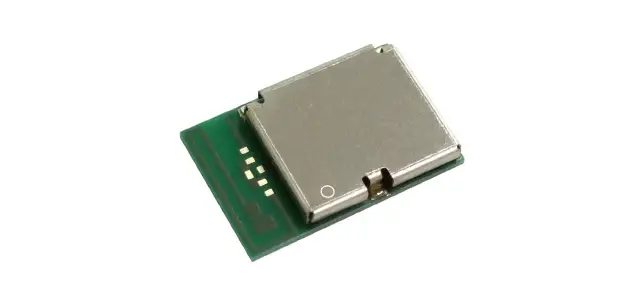
KAGA FEI ES2832 Bluetooth Module User Manual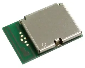
This module should be installed in the host device according to the interface specification.
- Japan Regulatory Information
a) This Product is a radio system and obtained certification of construction type combined with the specific antenna.
b) Please ensure that your product has a label with the following certification mark at easily viewable location. If your product is too small to have the label, please place it in the instruction manual and package of your product. The mark diameter shall be easily legible. In case your product does not have the label with the following certification mark, you or your customer who uses your product may be against the Radio Law and subjected to criminal punishment. KAGA FEI shall not be liable for any loss or damage incurred by you or your customer arising from use of your product which does not have following certification mark. This product installs a radio system which has been approved as a radio station in a low power data communication system based on the Radio Law.
ES2832 : 005-103118
005-103118 - Canada Regulatory Information
The following information must be indicated on the host device of this module;
a) This device complies with Innovation, Science and Economic Development Canada’s applicable licence-exempt RSSs. Operation is subject to the following two conditions:- This device may not cause interference; and
- This device must accept any interference, including interference that may cause undesired operation of the device.
- FCC Regulatory Information
a) This device complies with part 15 of the FCC Rules.- Part 15 Subpart C
b) The following statement shall be indicated on the host device or the user manual of the host device; Operation is subject to the following two conditions: (1) This device maynot cause harmful interference, and (2) this device must accept any interference received, including interference that may cause undesired operation. c) Please notify certified ID by either one of the following method on your product. - Contains Transmitter Module FCC ID: 2A6NFES2832
- Contains FCC ID: 2A6NFES2832
d) Since there is no space which indicates FCC ID on this module, FCC ID is indicated in a manual. If the FCC ID is not visible when the module is installed inside another device, then the module is installed must also display a label referring to the enclosed module.
e) The following statement shall be indicated in the user manual of the host device;
CAUTION: Changes or modifications not expressly approved by the party responsible for compliance could void the use’s authority to operate the equipment.
f) The modular transmitter is only FCC authorized for the specific rule parts (Part 15 Subpart C) listed on the grant, and the host product manufacturer is responsible for compliance to any other FCC rules that apply to the host not covered by the modular transmitter grant of certification. The final host product still requires Part 15 Subpart B compliance testing with the modular transmitter installed.
g) This product is certified as type of the portable device with FCC Rules. To maintain compliance with RF Exposure requirement, please use within specification of this product.
h) The following statement shall be indicated in the user manual of the host device; The antenna used for this transmitter must not be co-located or operating in conjunction with any other antenna or transmitter.
i) This module can change the output power depending on the circumstances by the application software which is developed by module installer. Any end user cannot change the output power.
j) Antenna List
No.1
Antenna Category: Monopole
Antenna Type: PCB antenna
Dimensions: 3.45mm x 2.85mm
- Part 15 Subpart C
- CE Regulatory Information
a) When your end product installs this module, it is required to proceed additional certification processes before placing on the market in EU member states to make your products fully comply with relative EU standards.
b) KAGA FEI can provide you the test reports of conducted measurement portion for the radio module. You can utilize the test reports for the certification processes of your end product as it requires radio testing.

Control No: Control name Pin Layout
Pin Descriptions
| Pin | Pin name | Pin function | Description |
| 1 | GND | Ground | Ground pin. (0 V) |
| 2 | P0.06 | Digital I/O | General purpose I/O pin. |
| 3 | P0.05AIN3 | Digital I/OAnalog input | General purpose I/O pin.SAADC/COMP/LPCOMP input. |
| 4 | P0.00XL1 | Digital I/OAnalog input | General purpose I/O pin.Connection for 32.768kHz crystal (LFXO). |
| 5 | P0.01XL2 | Digital I/OAnalog input | General purpose I/O pinConnection for 32.768kHz crystal (LFXO). |
| 6 | DCC | Power | DC/DC converter output pin. |
| 7 | DEC4 | Power | 1V3 regulator supply decoupling.Input from DC/DC converter. Output from 1.3 V LDO. |
| 8 | VCC_NRF | Power | Power supply pin. |
| 9 | P0.03AIN1 | Digital I/OAnalog input | General purpose I/O pin.SAADC/COMP/LPCOMP input. |
| 10 | P0.04AIN2 | Digital I/OAnalog input | General purpose I/O pin.SAADC/COMP/LPCOMP input. |
| 11 | OUT_ANT | Antenna In/Out | Internal antenna. It should be connected to Pin 12OUT_MOD for normal operation. |
| 12 | OUT_MOD | RF In/Out | RF I/O pin. It should be connected to Pin 11 OUT_ANT fornormal operation. |
| 13 | GND | Ground | Ground pin. (0 V) |
| 14 | NFCP0.09 | NFC inputDigital I/O | NFC antenna connection.General purpose I/O pin. |
| 15 | NFCP0.10 | NFC inputDigital I/O | NFC antenna connection.General purpose I/O pin. |
| 16 | SWDCLK | Digital input | Serial Wire Debug clock input for debug andprogramming |
| 17 | SWDIO | Digital I/O | Serial Wire Debug I/O for debug and programming |
| 18 | GND | Ground | Ground pin. (0 V) |
| 19 | P0.21 RESET | Digital I/O | General purpose I/O pinConfigurable as system RESET pin. (Factory default : GPIO) |
| 20 | P0.08 | Digital I/O | General purpose I/O pin. |
| 21 | P0.07 | Digital I/O | General purpose I/O pin. |
| 22 | P0.18TRACEDATA[0] | Digital I/O | General purpose I/O pinTrace port output. |
| Pin | Pin name | Pin function | Description |
| 23 | P0.02AIN0 | Digital I/OAnalog input | General purpose I/O pin.SAADC/COMP/LPCOMP input. |
| 24 | P0.28AIN4 | Digital I/OAnalog input | General purpose I/O pin.SAADC/COMP/LPCOMP input. |
| 25 | P0.20TRACECLK | Digital I/O | General purpose I/O pin.Trace port clock output. |
| 26 | GND | Ground | Ground pin. (0 V) |
| 27 | NC | Not Connected | Isolated pad on PCB for mechanical stability. |
| 28 | NC | Not Connected | Isolated pad on PCB for mechanical stability. |
![]()


