![]() Evaluating the ADCA5191 5 MHz to 1800 MHz Broadband CATV Amplifier
Evaluating the ADCA5191 5 MHz to 1800 MHz Broadband CATV Amplifier
EVAL-ADCA5191
UG-2041
User Guide
FEATURES
- 2-layer evaluation board with heat sink
- 75 Ω N-type RF male connectors
VALUATION KIT CONTENTS
- ADCA5191-EVALZ evaluation board
EQUIPMENT NEEDED
- RF signal generator
- RF spectrum analyzer
- DOCSIS signal generator
- DOCSIS signal analyzer
- RF network analyzer
- 8 V, 500 mA power supply
GENERAL DESCRIPTION
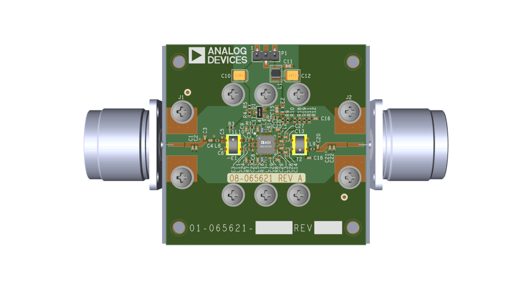
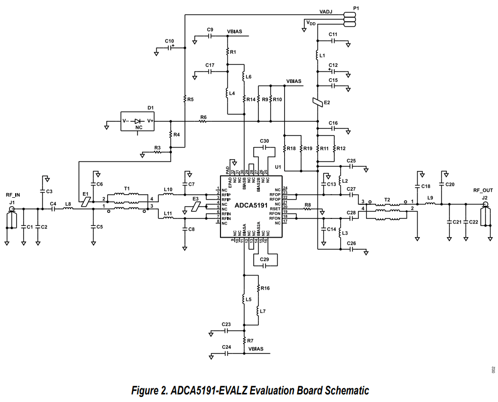
The ADCA5191-EVALZ evaluation board consists of a 2-layer printed circuit board (PCB) fabricated from a 62 mil laminate mounted to an aluminum heat sink. The heat sink assists in providing thermal relief to the device as well as mechanical support to the PCB. Mounting holes on the heat sink allow attachment to larger heat sinks for improved thermal management.
The ADCA5191-EVALZ is populated with components to interface the IC to a typical CATV application. J1 (RF_IN) and J2 (RF_OUT) are 75 Ω, N type, male coaxial connectors. The respective RF traces of the ports have a 75 Ω characteristic impedance. The ADCA5191-EVALZ is populated with components suitable for use over the −40 °C to +100 °C operating temperature range of the ADCA5191.
Access to the supply voltage (VDD) and GND is through a 3-pin header (P1) on the ADCA5191-EVALZ.
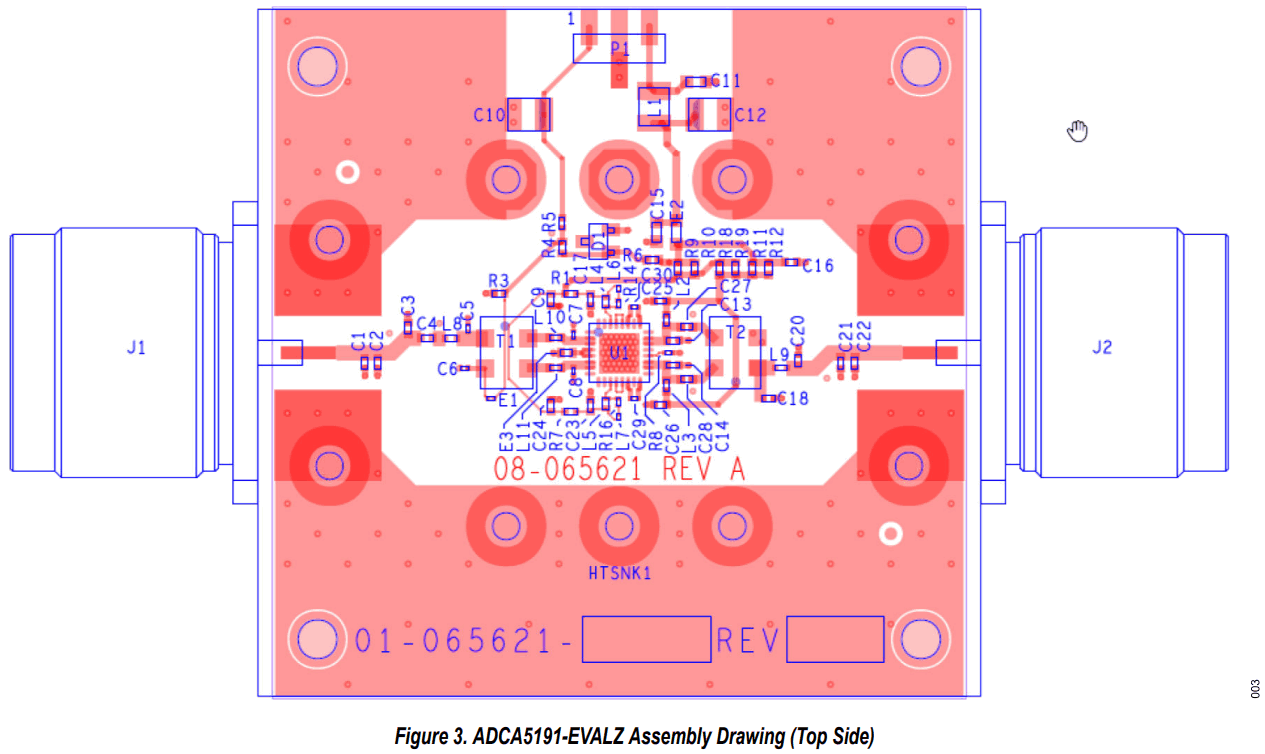
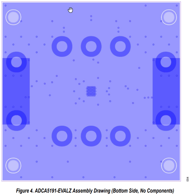
RF traces are 75 Ω microstrip at the input and output RF connectors. The package ground leads and the exposed paddle connect directly to the ground plane. Multiple vias connect the LFCSP ground paddle to the bottom ground plane to provide adequate electrical conduction and thermal conduction to the heat sink. The transfer of heat from the ADCA5191-EVALZ ground to the heat sink is further facilitated by the insertion of a piece of indium approximately the footprint of the LFCSP between the ADCA5191-EVALZ bottom and the heat sink. There are no components on the bottom side of the PCB.
Consult the ADCA5191 data sheet in conjunction with this user guide when using the ADCA5191-EVALZ evaluation board.
PLEASE SEE THE LAST PAGE FOR AN IMPORTANT WARNING AND LEGAL TERMS AND CONDITIONS.
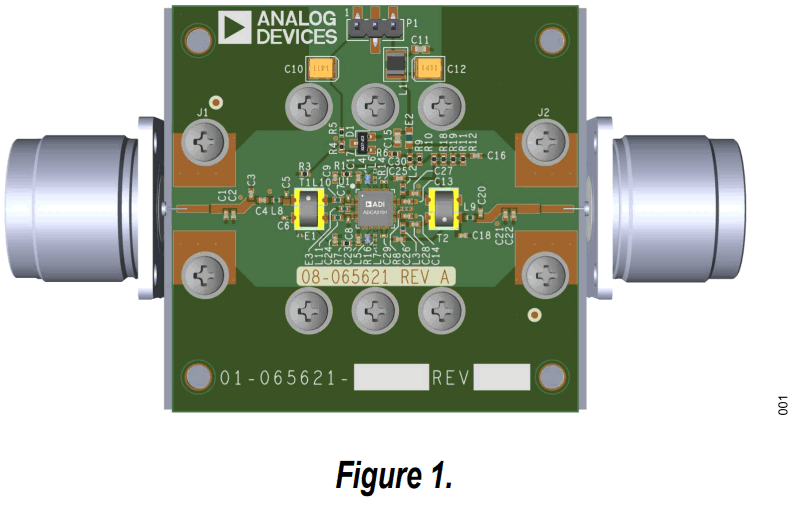
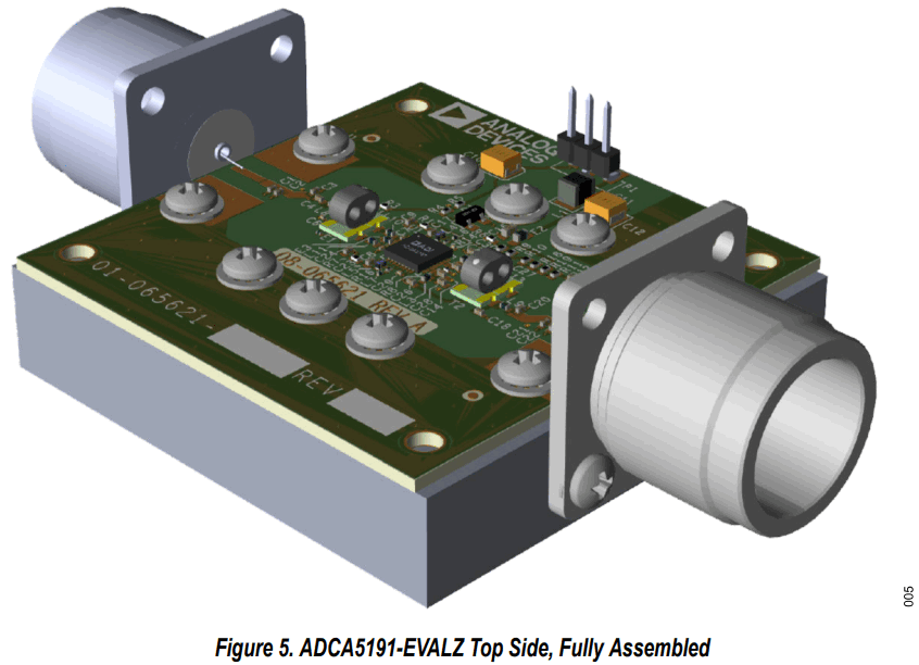
ADCA5191-EVALZ PHOTOGRAPH (TOP SIDE)
OPERATING THE ADCA5191-EVALZ
An 8 V, 500 mA power supply is required to provide the bias to the ADCA5191 on the ADCA5191-EVALZ. Connect the positive terminal of the 8 V power supply to the VDD pin on P1 and the ground terminal to the GND pin.
See the ADCA5191 data sheet for the typical dc supply current to expect when powering up the VDD supply. Consult the product data sheet for adjusting the bias current (IDD) by replacing R9 and R10.
RECOMMENDED BIAS SEQUENCES
During Power-Up
The recommended bias sequence during power-up follows:
- Set VDD to 8.0 V.
- Apply the RF signal.
During Power-Down
The recommended bias sequence during power-down follows:
- Turn off the RF signal.
- Set VDD to 0 V.
Table 1. Header Connections to the ADCA5191
| Connector | Header Pin | ADCA5191 Pin |
| P1 | 1 2 3 | Not used GND VDD |
RF Measurements
To evaluate the ADCA5191, connect a 75 Ω RF signal source to the N-type, male connector (J1), which can be a single-tone or multitone source for distortion measurements, or a wideband data over cable service interface specification (DOCSIS) signal source for analyzing modulation error ratio (MER) or bit error rate (BER) measurements. The input power must be <45 dBmV to produce an output power of <70 dBmV to support DOCSIS 3.0, DOCSIS 3.1, and DOCSIS 4.0 applications. The 75 Ω RF output signal is available on the N-type, male connector (J2) and can be interfaced directly to instruments (such as a spectrum analyzer or vector network analyzer) with a 75 Ω input impedance.
EVALUATION BOARD SCHEMATIC AND ASSEMBLY DRAWINGS
 |  |
 | |
ADCA5191-EVALZ ASSEMBLY INFORMATION
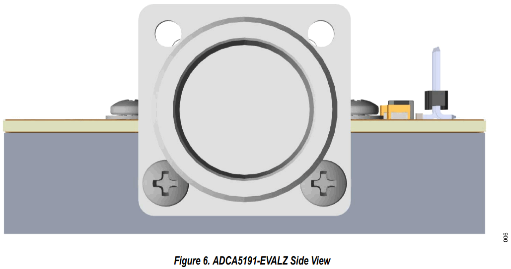
The PCB for the ADCA5191-EVALZ is assembled using normal manufacturing practices, excluding the J1 and J2 connectors, and the custom external aluminum heat sink. Once the PCB is assembled, it is mounted with 10 screws to the external heat sink as shown in Figure 5. The transfer of heat from the ADCA5191-EVALZ ground to the heat sink is enhanced by the insertion of a thin sheet of indium cut to approximately the footprint of the ADCA5191 and located between the via array on the bottom of the PCB (underneath the ADCA5191) and the heat sink. The J1 and J2 connectors are then mounted to the heat sink using two screws for each (see Figure 6). Then, the center conductor for the RF connectors is soldered to the PCB. Once complete, the ADCA5191-EVALZ is ready for testing.
 |  |
ORDERING INFORMATION
BILL OF MATERIALS
Table 2. Bill of Materials¹
| Reference Designator | Value | Tolerance | Minimum Rating | Footprint | Suggested Vendor | Suggested Part Number |
| C3 | 0.4 pF | ±0.1 pF | 50 V | 402 | Murata | GRM1555C2AR40BA1D |
| C5 | 0.6 pF | ±0.1 pF | 100 V | 201 | Murata | GRM0335C2AR60BA01D |
| C6 | 0.01 μF | 10% | 50 V | 201 | Taiyo Yuden | UMK063BJ103KP-F |
| C7, C8 | 0.5 pF | ±0.1 pF | 100 V | 402 | Murata | GRM1555C2AR50BA01D |
| C11 | 0.01 µF | 20% | 100 V | 603 | TDK | C1608X7R2A103M080AA |
| C12 | 2.2 µF | 10% | 50 V | 1210 | Kyocera AVX | TAJB225K050RNJ |
| C13, C14 | 0.6 pF | ±0.1 pF | 100 V | 402 | Murata | GRM1555C2AR60BA01D |
| C15 | 0.047 µF | 10% | 50 V | 603 | TDK | 06035C473KAT4A |
| C27, C28 | 160 pF | 1% | 50 V | 402 | Murata | GRT1555C1H161FA02D |
| C4, C9, C16, C17, C23, C24, C25, C26 | 0.01 µF | 10% | 100 V | 402 | TDK | 810-C1005X7S2A103K |
| E1 | 1000 Ω ferrite | 25% | 170 mA | 201 | Murata | BLM03BX102SN1D |
| E2 | 220 Ω ferrite | 25% | 1.8 A | 603 | Taiyo Yuden | FBMH1608HM221-T |
| J1, J2 | 75 Ω | N/A | N/A | N/A | Pasternack | PE4503 |
| L1 | 2.2 uH | 20% | 1.6 A | 1210 | Taiyo Yuden | BRL3225T2R2M |
| L2, L3 | 270 nH | 5% | 590 mA | 402 | Coilcraft | 0402DF-271XJRW |
| L4, L5 | 470 nH | 5% | 610 mA | 603 | Coilcraft | 0603AF-471XJEW |
| L6, L7 | 10 nH | 3% | 250 mA | 201 | Murata | LQP03TN10NH02D |
| L8 | 5.6 nH | 0.2 nH | 800 mA | 402 | Murata | LQW15AN5N6C10D |
| L9, L10, L11, R11, R12 | 0 Ω | N/A | 0.1 W | 402 | Panasonic | ERJ-2GE0R00X |
| R1, R7 | 10 Ω | 1% | 0.1 W | 402 | Panasonic | ERJ-2RKF10R0X |
| R4, R6 | 365 Ω | 1% | 62.5 mW | 402 | Yageo | RC0402FR-07365RL |
| R8 | 2 kΩ | 1% | 50 mW | 201 | Panasonic | ERJ-1GNF2001C |
| R9, R10 | 33 Ω | 1% | 200 mW | 402 | Vishay | CRCW040233R0FKEDHP |
| R14, R16 | 120 Ω | 1% | 50 mW | 201 | Panasonic | ERJ-1GNF1200C |
| T1, T2 | 1:1 transformer | N/A | N/A | 99-01-16182 | Mini-Circuits | TRS1-182-75-3+ |
| U1 | CATV amplifier | N/A | N/A | 5 mm × 5 mm, 32-lead LFSCP | Analog Devices, Inc. | ADCA5191 |
| P1 | 3 pin header | N/A | N/A | 0.100″ | Molex | 087898-0306 |
| C1, C2, C9, C10, C17, C18, C20, C21, C22, C23, C24, C29, C30, D1, E3, R1, R3, R5, R7, R14, R16, R18, R19 | Do not install | N/A | N/A | N/A | N/A | N/A |
¹N/A means not applicable.
NOTES
……………………………..![]() ESD Caution
ESD Caution
ESD (electrostatic discharge) sensitive device. Charged devices and circuit boards can discharge without detection. Although this product features patented or proprietary protection circuitry, damage may occur on devices subjected to high energy ESD. Therefore, proper ESD precautions should be taken to avoid performance degradation or loss of functionality.
Legal Terms and Conditions
By using the evaluation board discussed herein (together with any tools, components documentation or support materials, the “Evaluation Board”), you are agreeing to be bound by the terms and conditions set forth below (“Agreement”) unless you have purchased the Evaluation Board, in which case the Analog Devices Standard Terms and Conditions of Sale shall govern. Do not use the Evaluation Board until you have read and agreed to the Agreement. Your use of the Evaluation Board shall signify your acceptance of the Agreement. This Agreement is made by and between you (“Customer”) and Analog Devices, Inc. (“ADI”), with its principal place of business at Subject to the terms and conditions of the Agreement, ADI hereby grants to Customer a free, limited, personal, temporary, non-exclusive, non-sublicensable, non-transferable license to use the Evaluation Board FOR EVALUATION PURPOSES ONLY. Customer understands and agrees that the Evaluation Board is provided for the sole and exclusive purpose referenced above, and agrees not to use the Evaluation Board for any other purpose. Furthermore, the license granted is expressly made subject to the following additional limitations: Customer shall not (i) rent, lease, display, sell, transfer, assign, sublicense, or distribute the Evaluation Board; and (ii) permit any Third Party to access the Evaluation Board. As used herein, the term “Third Party” includes any entity other than ADI, Customer, their employees, affiliates and in-house consultants. The Evaluation Board is NOT sold to Customer; all rights not expressly granted herein, including ownership of the Evaluation Board, are reserved by ADI. CONFIDENTIALITY. This Agreement and the Evaluation Board shall all be considered the confidential and proprietary information of ADI. Customer may not disclose or transfer any portion of the Evaluation Board to any other party for any reason. Upon discontinuation of use of the Evaluation Board or termination of this Agreement, Customer agrees to promptly return the Evaluation Board to ADI. ADDITIONAL RESTRICTIONS. Customer may not disassemble, decompile or reverse engineer chips on the Evaluation Board. Customer shall inform ADI of any occurred damages or any modifications or alterations it makes to the Evaluation Board, including but not limited to soldering or any other activity that affects the material content of the Evaluation Board. Modifications to the Evaluation Board must comply with applicable law, including but not limited to the RoHS Directive. TERMINATION. ADI may terminate this Agreement at any time upon giving written notice to Customer. Customer agrees to return to ADI the Evaluation Board at that time. LIMITATION OF LIABILITY. THE EVALUATION BOARD PROVIDED HEREUNDER IS PROVIDED “AS IS” AND ADI MAKES NO WARRANTIES OR REPRESENTATIONS OF ANY KIND WITH RESPECT TO IT. ADI SPECIFICALLY DISCLAIMS ANY REPRESENTATIONS, ENDORSEMENTS, GUARANTEES, OR WARRANTIES, EXPRESS OR IMPLIED, RELATED TO THE EVALUATION BOARD INCLUDING, BUT NOT LIMITED TO, THE IMPLIED WARRANTY OF MERCHANTABILITY, TITLE, FITNESS FOR A PARTICULAR PURPOSE OR NONINFRINGEMENT OF INTELLECTUAL PROPERTY RIGHTS. IN NO EVENT WILL ADI AND ITS LICENSORS BE LIABLE FOR ANY INCIDENTAL, SPECIAL, INDIRECT, OR CONSEQUENTIAL DAMAGES RESULTING FROM CUSTOMER’S POSSESSION OR USE OF THE EVALUATION BOARD, INCLUDING BUT NOT LIMITED TO LOST PROFITS, DELAY COSTS, LABOR COSTS OR LOSS OF GOODWILL. ADI’S TOTAL LIABILITY FROM ANY AND ALL CAUSES SHALL BE LIMITED TO THE AMOUNT OF ONE HUNDRED US DOLLARS ($100.00). EXPORT. Customer agrees that it will not directly or indirectly export the Evaluation Board to another country, and that it will comply with all applicable United States federal laws and regulations relating to exports. GOVERNING LAW. This Agreement shall be governed by and construed in accordance with the substantive laws of the Commonwealth of Massachusetts (excluding conflict of law rules). Any legal action regarding this Agreement will be heard in the state or federal courts having jurisdiction in Suffolk County, Massachusetts, and Customer hereby submits to the personal jurisdiction and venue of such courts. The United Nations Convention on Contracts for the International Sale of Goods shall not apply to this Agreement and is expressly disclaimed.
©2022 Analog Devices, Inc. All rights reserved. Trademarks and registered trademarks are the property of their respective owners.
One Analog Way, Wilmington, MA 01887-2356, U.S.A.
analog.com
Rev. 0
EVAL-ADCA5191


