![]() NCP1680 – Totem Pole CrM Controller Evaluation
NCP1680 – Totem Pole CrM Controller Evaluation
Board User’s Manual
EVBUM2822/D
Introduction
The NCP1680 is a Critical Conduction Mode (CrM) Power Factor Correction (PFC) controller IC designed to drive the bridgeless Totem Pole PFC (TPFC) topology. The bridgeless totem pole PFC consists of two totem pole legs:
a fast switching leg driven at the PWM switching frequency and a second leg that operates at the AC line frequency. This topology eliminates the diode bridge present at the input of a conventional PFC circuit, allowing significant improvement in efficiency and power density.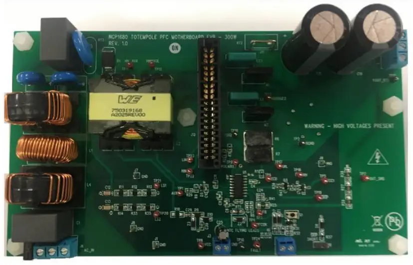 Figure 1. NCP1680 Evaluation Board
The NCP1680 Evaluation Board (EVB) user guide demonstrates a universal line, 300 W totem pole PFC built using NCP1680. NCP1680 is intended for Industrial power supplies, Telecom/5G/Networking power, USB PD, Gaming consoles, UHD TV power supplies, and Lighting applications. TPFC topology eliminates the need for heatsinks or forced air in the NCP1680 EVB while operating at an ambient of 25°C.
Table 1. KEY SPECIFICATIONS
| Description | Value | Unit |
| Input Voltage Range | 90−265 | Vac |
| Line Frequency Range | 47−63 | Hz |
| Output Voltage | 395 | V |
| Output Power | 300 | W |
| Output Ripple | < 5 | % |
| PF @ Full Load | > 0.95 | |
| THD @ Full Load | < 10 | % |
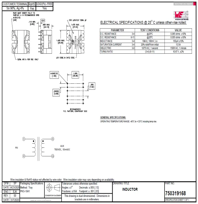
| Inductor Value | 150 | μH |
| Inductor Core Size/Geometry | PQ3220 | |
| Bulk Capacitor Value | 200 | μF |
| Maximum Frequency | 130 | kHz |
NOTE: NCP1680 EVB is a high voltage demonstration board. It can accept an input voltage of 90 Vac to 265 Vac and the output voltage of the board is 395 Vdc nominally. This EVB is for demonstration purposes only and should not be used to power any loads other than an electronic load. Only trained professionals in using high voltage equipment should handle the board and appropriate safety precautions should be followed.
TYPICAL APPLICATION SCHEMATIC
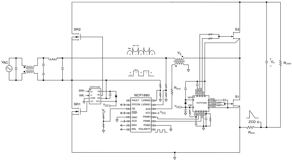 Figure 2. Typical Application Schematic of a CrM Totem Pole PFC Utilizing NCP1680
As shown in Figure 2, the slow leg switches (SR1 & SR2) are high voltage silicon−based FETs, also known as super junction (SJ) FETs, and the fast leg switches (S1 & S2) are Enhancement−mode Gallium Nitride (eGaN) devices. Since NCP1680 employs a CrM control architecture where the inductor current resets back to zero before the next switching cycle, low reverse recovery charge (Qrr) SJ FETs can also be utilized for the fast leg albeit with slightly inferior performance, but better cost structure. As a controller the NCP1680 is agnostic to the fast leg switch technology. Wide−Bandgap (WBG) devices such as Silicon Carbide (SiC) or eGaN are recommended for optimal performance. SiC is a good choice for lower frequency applications while eGaN is an excellent choice for both low frequency and high frequency applications.
The NCP1680 evaluation board is designed such that engineers interested in this novel topology can easily probe various signals and learn the intricacies of TPFC. The fast leg half bridge is implemented on a daughter card where the fast leg switches are driven using NCP51820, a high voltage eGaN half−bridge driver; the slow leg switches are driven using NCP51530, a high voltage Si FET half−bridge driver.
The NCP1680 employs a novel current limit scheme where a simple resistor placed in the return path between bulk ground and the IC ground, is utilized for current limiting.
The Zero Current Detection (ZCD) resistor is further utilized for drive control of the synchronous switch in the fast leg.
Additionally, the NCP1680 requires only a single auxiliary winding to sense switch node valleys (in positive half−line cycle) and switch node peaks (in negative half line cycle). This novel scheme results in the main boost switch being turned on with minimal voltage across the switch improving efficiency and reducing EMI.
BOARD DESCRIPTION AND TEST SETUP
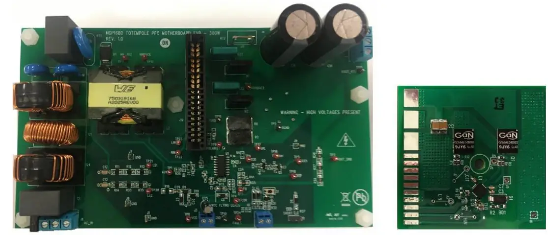 Figure 3. NCP1680 Evaluation Board along with a Daughter Card Featuring Fast Leg Switches
The evaluation motherboard and daughter card are shown in Figure 3. The motherboard includes multiple I/O connectors and test points to simplify instrumentation and waveform capture during the evaluation process. A brief description and pinout of the I/O connectors is shown in Table 2, and a listing of the test points plus the respective circuit node is shown in Table 3.
There are some key points worth mentioning regarding the I/O connectors and test points:
- The pins labeled GND and VOUT_RTN are NOT electrically common. GND and VOUT_RTN are physically separated by the ZCD resistor and the user should take precaution to not short these two nodes together. For example, the ground lead of an Earth−connected oscilloscope probe should not be simultaneously connected to both GND and VOUT_RTN.
- The EVB requires an external VCC bias supply. It is recommended to connect this bias supply at the J3 connector or across the TP8−TP10 test points. The recommended operating range for VCC is 12–18 V with a current sourcing capability greater than 10 mA. Once the EVB has been enabled, VCC can fall as low as 9 V before the NCP1680 UVLO circuit disables the controller. A VCC voltage greater than 20 V will trip the EVB over−voltage protection (OVP) and latch off the controller.
- J6 – AC Input connector is pinned out for a 3−wire AC input connection. However, the chassis GND connection is not required and can be left open. The user should determine the appropriate input connection based on their application requirements.
- J10 – SKIP header should be open to allow normal operation of the EVB. Placing a jumper across the J10 header will force the EVB into Skip/Standby mode operation, described later.
- J11 – Inrush current limiter (ICL) bypass is populated by default. If the user wishes to operate the NCP1680 EVB with an ICL then J11 must be removed before populating the ICL at REF DES RT2.
- J12 – Daughter card interface is not keyed. User should take precaution that the daughter card is correctly oriented into J12. Furthermore, user must take precaution that the daughter card is never inserted or removed while VCC is applied to the motherboard, doing so can damage EVB.
Table 2. I/O CONNECTOR DESCRIPTIONS
| REF DES | Function | Pinout |
| J1, J7, J8, J9 | GND Peg | 1. GND |
| J2 | DC Output Voltage | 1. VOUT_RTN 2. N/C 3. VOUT |
| J3 | VCC | 1. VCC 2. GND |
| J4 | PFCOK Skip Interface | 1. CNTRL Signal 2. GND |
| J6 | AC Input Voltage | 1. AC Line 2. Chassis GND 3. AC Neutral |
| J10 | SKIP Control Header | 1. CNTRL 2. GND |
| J11 | Inrush Current Limit Bypass | 1. VOUT_NTC 2. VOUT |
| J12 | Daughter Card Interface | 1−6: VOUT_NTC 7−12: VBRIDGE 13−18: PWRGND 19−28: N/C 29−32: GND 33−34: PWML/LIN 35−36: PWMH/HIN 37−38: VCC |
Table 3. TEST POINT DESCRIPTIONS
| REF DES | Node | REF DES | Node |
| TP1 | NCP1680 AUX Pin | TP13 | Slow Leg Bridge Node |
| TP2 | GND @ NCP51530 Driver | TP14 | VOUT |
| TP3 | NCP1680 FB Pin | TP15 | VOUT_RTN |
| TP4 | NCP1680 PFCOK Pin | TP16 | NCP1680 SRH |
| TP5 | NCP51530 VCC1 | TP17 | NCP1680 SRL |
| TP6 | NCP1680 ZCD Pin | TP18 | PWRGND |
| TP7 | VOUT_SNS | TP19 | NCP1680 SKIP Pin |
| TP8 | NCP1680 VCC Pin | TP20 | NCP1680 LVSNS2 Pin |
| TP9 | NCP1680 Polarity Pin | TP21 | NCP1680 LVSNS1 Pin |
| TP10 | GND @ J3 Connector | TP22 | NCP1680 PWMH/HIN |
| TP11 | Haversine @ L2 Inductor | TP23 | NCP1680 PWML/LIN |
| TP12 | Fast Leg Bridge Node | TP24 | NCP1680 Fault Pin |
In order to replicate the data published in this design note, the following test set up is recommended:
- For higher power measurements (> 10% load), always arrange the connection so that the voltmeters at input and output are as close to NCP1680 evaluation board (UUT) as possible to avoid power loss due to resistance of the wiring or any other instrumentation.
- For input power measurement, please read power measurement directly from the power meter. Do not multiply VAC and IAC measurements, this is the apparent power of UUT. The power measurement provides the real power consumed by the UUT.
- Do not use the electronic load reading for output voltage measurement. A separate DMM placed directly across output (TP14−TP15) will produce a more accurate reading than the eLoad and cancels some of the instrumentation power loss in ammeter.
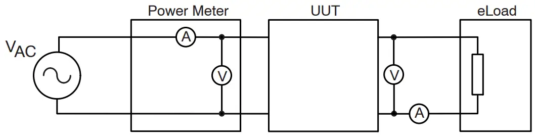 Figure 4. Test Setup for NCP1680 EVB
PERFORMANCE CHARACTERISTICS – DATA AND WAVEFORMS
Efficiency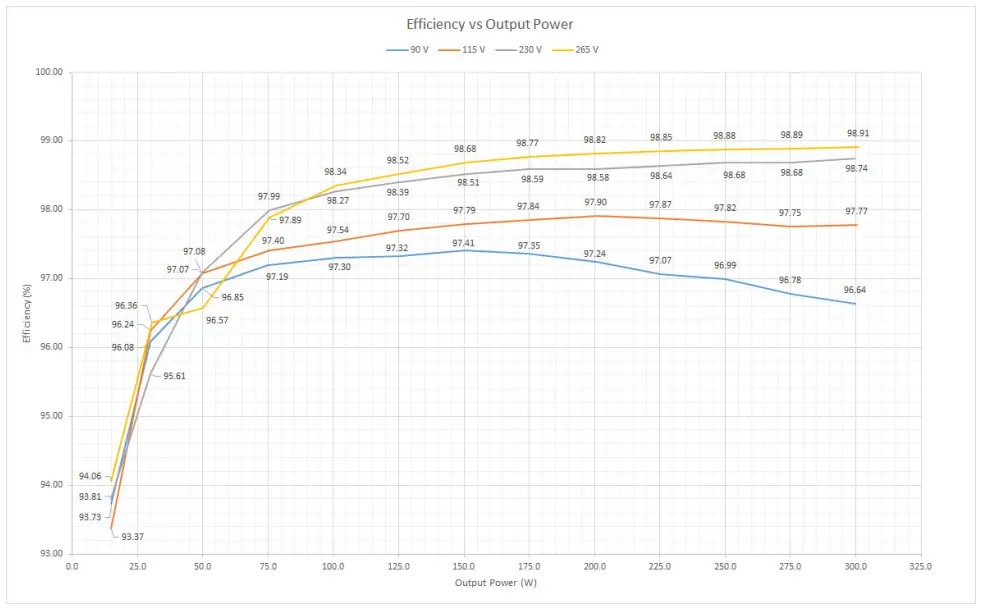 Figure 5. Efficiency vs. Output Power
Power Factor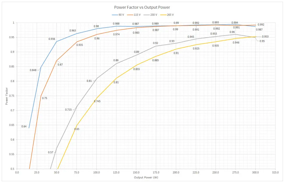 Figure 6. Power Factor vs. Output Power
Total Harmonic Distortion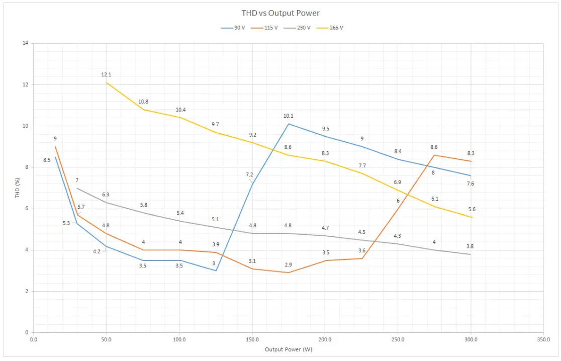 Figure 7. THD vs. Output Power
Switching Frequency at the Peak of AC Line vs. Output Power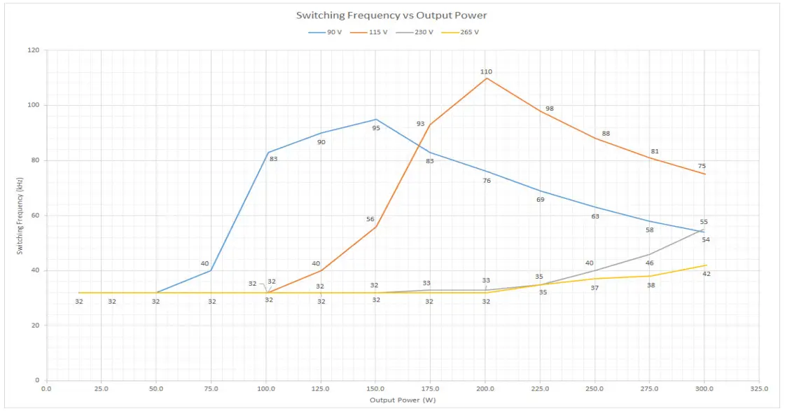 Figure 8. Switching Frequency vs. Output Power
Soft−Start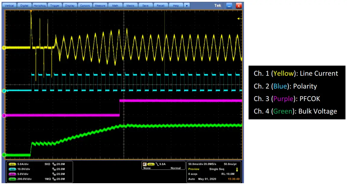 Figure 9. Soft−Start
Load Transient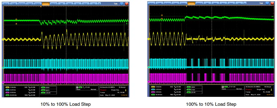 In the above waveforms, NCP1680’s dynamic response enhancer (DRE) limits the lower bulk voltage to 367 V while the output overvoltage protection (OVP) limits the upper bulk voltage to 418 V. Transient data was captured at 115 Vac.
 Figure 10. Load Transient
Input Current Waveforms and Output Ripple at Various Line Voltages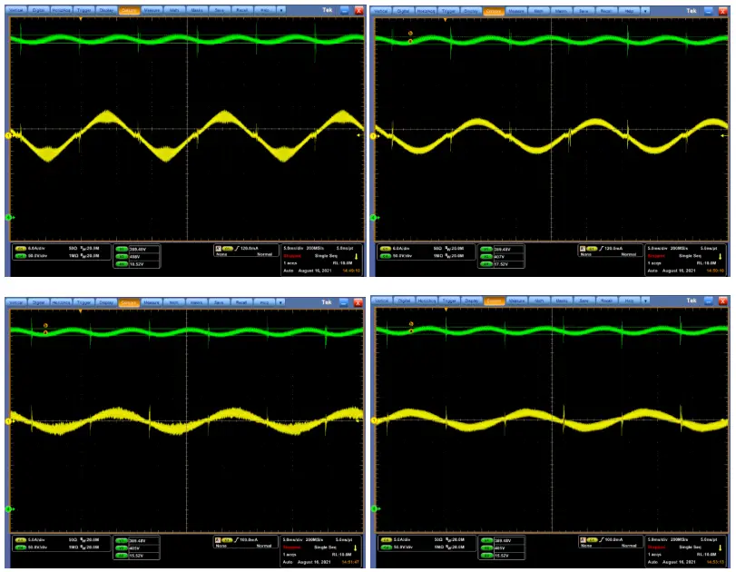 Figure 11. Input Current Waveforms and Output Ripple at Various Line Voltages
Skip/Standby Mode Control
The NCP1680 features a Skip/Standby mode which enables the application to achieve very good no−load and light−load performance. The device must be externally commanded to enter the Skip mode by pulsing the PFCOK pin or grounding the SKIP pin, and in a typical application this control signal would be provided by a downstream DC−DC converter. For the NCP1680 motherboard, additional circuitry shown in Figure 12 has been designed in to allow the user to easily transition the EVB into the Skip/Stanbdy mode without the use of a downstream converter.
The J10 header which is a standard 2 position, 100 mil pitch connector header, provides a path to GND for the SKIP pin. The user can operate the EVB in Skip mode by placing a mating jumper (such as TE Connectivity 382811−6) across the header, grounding the SKIP pin. J10 is conveniently located on the PCB away from any high voltage nodes so that the jumper can be placed while the EVB is in live operation. Nonetheless, the user should exercise caution when placing this jumper to prevent injury to themselves or damage to the EVB.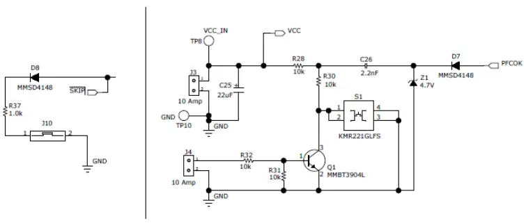 Figure 12. NCP1680 EVB Skip Interfaces
The second skip interface on the EVB is at the J4 connector which can be used to connect in a function generator to pulse the PFCOK pin. For the NCP1680 to enter skip mode the PFCOK pin must be pulsed below 400 mV for a duration greater than 50 us as is shown in Figure 13. It is recommended that the function generator output be a signal with 0–5 V amplitude where the output remains at 5 V for at least 100 us to meet the threshold requirements on the PFCOK pin.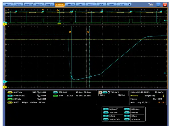 Figure 13. PFCOK Skip−Entry Signal (Ch1 = Bulk Voltage, Ch2 = PFCOK, Ch4 = SKIP)
Once skip mode has been entered the NCP1680 controller will regulate the bulk voltage with a form of hysteretic control, meaning that the bulk voltage will cycle between its nominal regulation voltage and ~94% of nominal regulation. The frequency at which the bulk voltage cycles will be dependent on the output load. To maintain the EVB in skip/standby mode it is necessary to continue pulsing the PFCOK pin wherein every PFCOK pulse must meet the previously stated voltage and timing threshold requirements. The pulse frequency to maintain skip mode must be faster than the frequency at which the bulk voltage cycles between nominal regulation and 94% of nominal regulation. Hence it is technically possible to operate the EVB in skip mode at any load level and often in applications, skip operation may be necessary up to 5–10% of the rated load. Figure 14 shows skip mode operation with the EVB loaded at 20 W. A lighter load, or no load will result in much longer cycle frequency and better performance.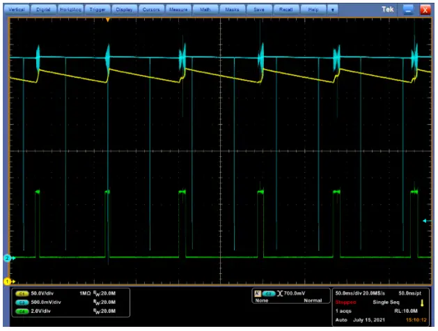 Figure 14. NCP1680 Skip Mode Operation (Ch1 = Bulk Voltage, Ch2 = PFCOK, Ch4 = SKIP)
Control Loop Measurement
The NCP1680 controller is embedded with an internal compensator circuit which provides the necessary loop bandwidth to ensure good power factor performance, and also provides sufficient phase & gain margin at the loop crossover frequency to ensure stable and robust operation of the application. Verification of the control loop characteristics is a good practice for any power supply design. The NCP1680 motherboard provides a 1 kΩ injection resistor and test points (TP14, TP7) around the injection resistor enabling the use of a network analyzer with an isolated injection transformer to measure the loop response of the EVB. Figure 15 shows the loop response of the NCP1680 EVB with 300 W load, measured at 115 VAC and 230 VAC. The loop bandwidth measures from ~ 8–11 Hz with about 70° of phase margin and > 14 dB of gain margin.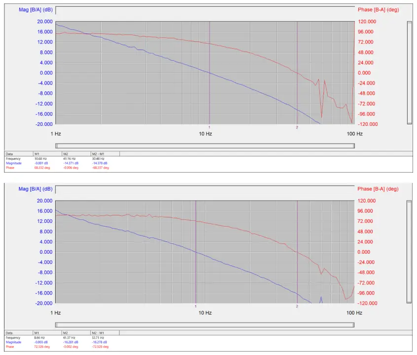 Figure 15. EVB Bode Plots @ 300 W; 115 V on Top; 230 V on Bottom
Thermal Performance
The NCP1680 EVB and daughter card where also evaluated for thermal performance while operating at 90 VAC and 300 W. Thermal images of the fast leg GaN HEMTs, the boost inductor, and the slow leg silicon FETs are shown in Figure 16. These images were captured in a25°C ambient environment with no external air flow. The high efficiency performance of the TPFC is evident in the device temperatures where the fast and slow leg switches measure below 60°C, a modest 35°C rise above room temperature. The daughter card PCB is also designed in a manner that eliminates the need for an additional heatsink to be mounted to the board. The PCB’s internal copper planes function as heat sinking and the temperature rise of the fast leg switches is well controlled by these copper planes.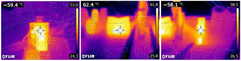 Figure 16. Thermal Measurement of Fast Leg eGaN Switches, Boost Inductor, and Slow leg Si FETs
MOTHERBOARD PCB ARTWORK
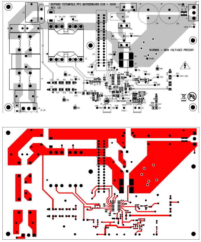 Figure 17. Motherboard PCB (Part 1/3)
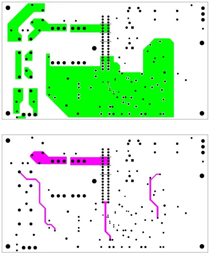 Figure 18. Motherboard PCB (Part 2/3)
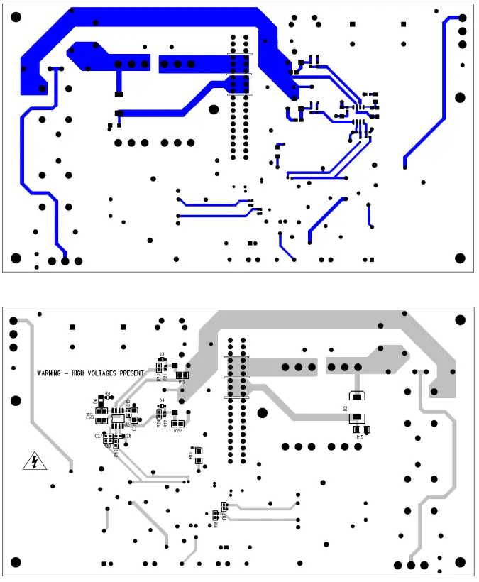 Figure 19. Motherboard PCB (Part 3/3)
DAUGHTERBOARD PCB ARTWORK
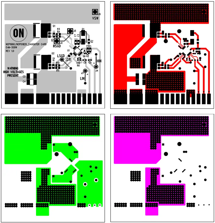 Figure 20. Daughterboard PCB (Part 1/2)
 Figure 21. Daughterboard PCB (Part 2/2)
TRANSFORMER DATA SHEET
SCHEMATIC
Motherboard Control Section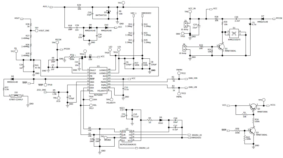 Figure 23. Motherboard Control Section
Motherboard Power Train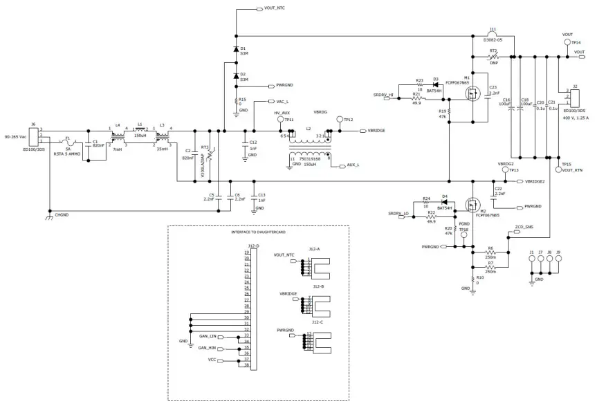 Figure 24. Motherboard Power Train
Daughter Card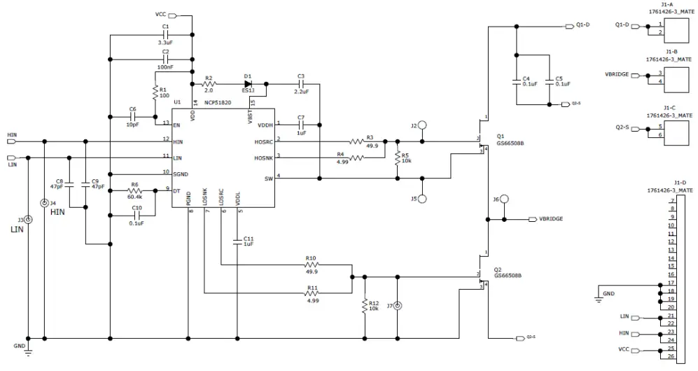 Figure 25. Daughter Card
BILL OF MATERIALS
Table 4. BILL OF MATERIALS – MOTHERBOARD
| Item | Qty | REF DES | Value | Description | Manufacturer | MPN | PCB Footprint | Substitution Allowed |
| 1 | 1 | C7 | 1 nF | CAP CER 1000 pF 50 V C0G/NP0 0603 | Kemet | C0603X102J5GAC7867 | 603 | Yes |
| 2 | 1 | C10 | 22 pF | CAP CER, NPO 22 pF 50 V | Wurth | 885012006053 | 603 | Yes |
| 3 | 1 | C11 | 0.1 µF | CAP CER 0.1 µF 50 V 10% X7R 0603 | Murata | GCM188R71H104KA57D | 603 | Yes |
| 4 | 1 | C14 | 10 n | CAP CER 10 nF 50 V X7R 0603 | Yageo | CC0603KRX7R9BB103 | 603 | Yes |
| 5 | 1 | C15 | 0.1 µF | CAP CER 0.1 µF 50 V 10% X7R 0603 | Murata | GCM188R71H104KA57D | 603 | Yes |
| 6 | 1 | C17 | 0.1 µF | CAP CER 0.1 µF 50 V 10% X7R 1206 | Kemet | C1206C104K5RACAUTO | 1206 | Yes |
| 7 | 1 | C19 | 10 µF | CAP CER 10 µF 25 V 10% X7R 1206 | Samsung | CL31B106KAHNNNE | 1206 | Yes |
| 8 | 1 | C25 | 22 µF | CAP ALUM 22 µF 20% 50 V RADIAL | Nichicon | UVK1H220MDD1TD | Radial | Yes |
| 9 | 1 | C29 | 22 nF | CAP CER 22 nF 50 V X7R 0603 | Kemet | C0603C223K5RACTU | 603 | Yes |
| 10 | 1 | C30 | 1 µF | CAP CER 1 µF 25 V 10% X7R 0603 | Samsung | CL10B105KA8NNNC | 603 | Yes |
| 11 | 1 | C31 | 22 µF | CAP CER 22 µF 25 V 10% X5R 1206 | Samsung | CL31A226KAHNNNE | 1206 | Yes |
| 12 | 2 | C1−2 | 820 nF | Cap, X Type, 275 V, AC, Polypropylene | Kemet | R46KI382040P0 | MBox, Radial | No |
| 13 | 2 | C12−13 | 1 nF | CAP CER 1 nF 630 V X7R 1206 | Yageo | CC1206KKX7RZBB102 | 1206 | Yes |
| 14 | 2 | C16, C18 | 100 µF | CAP ALUM 100 µF 20% 450 V Rad. 18 x 40 mm | United Chemi−Con | EKXG451ELL101MM40S | Round, Radial | Yes |
| 15 | 2 | C20−21 | 0.1 µF | CAP CER 0.1 µF 630 V 10% X7R 1210 | Kemet | C1210C104KBRAC7800 | 1210 | Yes |
| 16 | 2 | C22−23 | 2.2 nF | CAP FILM 2200 pF 20% 1.25 kVDC RAD | Kemet | PHE850EA4220MA01R17 | Radial, 13 x 4 mm | No |
| 17 | 1 | C24 | 1 nF | CAP CER 1000 pF 50 V C0G/NP0 0603 | Kemet | C0603X102J5GAC7867 | 603 | Yes |
| 18 | 1 | C26 | 2.2 nF | CAP CER 2200 pF 50 V X7R 0603 | Kemet | C0603C222M5RACTU | 603 | Yes |
| 19 | 2 | C27−28 | DNP | CAP CER DNP Placeholder 0603 | NA | NA | 603 | No |
| 20 | 3 | C4, C8−9 | 220 pF | CAP CER 220 pF C0G/NPO 0603 | Kemet | C0603C221J5GACTU | 603 | Yes |
| 21 | 2 | C5−6 | 2.2 nF | Cap, Disc, Y Type, 760 VAC | Kemet | C961U222MWWDBA7317 | Box, Axial | No |
| 22 | 1 | D6 | ES1J | Diode Ultrafast 600 V SOD−123−FL | onsemi | ES1JFL | SOD−123_ FL | No |
| 23 | 2 | D1−2 | S3M | Diode GEN PURP 1 kV 3A | onsemi | S3M | SMC | No |
| 24 | 3 | D3−5 | BAT54H | Diode Schottky 30 V 200 mA (DC) Surface MountSOD−323 | onsemi | BAT54HT1G | SOD−323_ rev3 | Yes |
| 25 | 4 | D7−10 | MMSD4148 | DIODE GEN PURP 100 V 200 mA SOD123 | onsemi | MMSD4148T1G | SOD−123 | Yes |
| 26 | 1 | F1 | 5A | Fuse, 8.4 x 4 mm,5.08 mm spacing | Bel Fuse | RSTA 5 AMMO | Thru−Hole | Yes |
| 27 | 1 | J10 | Connector, Header, 100Mil spacing | Amphennol | 67997−224HLF | Thru−Hole | Yes | |
| 28 | 1 | J11 | Jumper, 1 mm dia. 10.16 mm, Gold | Harwin | D3082−05 | Thru−Hole | Yes |
Table 4. BILL OF MATERIALS – MOTHERBOARD (continued)
| Item | Qty | REF DES | Value | Description | Manufacturer | MPN | PCB Footprint | Substitution Allowed |
| 29 | 1 | J12 | Conn, Edge, Dual, Female, 26 Position | TE Connectivity | 1761426−3 | Thru−Hole, 26 pos | Yes | |
| 30 | 4 | J1, J7−9 | Testpin, Gold, 40mil | Mill−Max | 3103−2−00−21−00−00− 08−0 | SIP−1 | Yes | |
| 31 | 2 | J2, J6 | Header, Vert. 3 pin, 5 mm Spacing | OST | ED100/3DS | Thru−Hole | Yes | |
| 32 | 2 | J3−4 | 10 Amp | 2 Position Wire to Board Terminal Block Horizontal with Board 0.138” (3.5 mm) LS | Phoenix Contact | 1984617 | TBD | Yes |
| 33 | 1 | L1 | 150 µH | Inductor, Differential, 150 µH, 5.4 A_42mΩ | Wurth | 7447055 | Thru−Hole | No |
| 34 | 1 | L2 | 150 µH | PFC Inductor, AUX, 150 µH, 3 A, Np:Naux = 10:1 | Wurth | 750319168 | PQ3230 | No |
| 35 | 1 | L3 | 35 mH | Common Mode Choke, 2x 35 mH, 2x 80 mΩ, 3.5 A | Wurth | 7448040435 | Thru−Hole | No |
| 36 | 1 | L4 | 7 mH | Common Mode Choke, 2x 7 mH, 2x 20 mΩ, 7 A | Wurth | 7448040707 | Thru−Hole | No |
| 37 | 2 | M1−2 | MOSFET N CH 650 V 44A TO−220F | onsemi | FCPF067N65S3 | TO−220 | No | |
| 38 | 5 | MT1−5 | HEX STANDOFF #6−32 NYLON 3/4” | Keystone | 1903D | NA | Yes | |
| 39 | 5 | MT1−5 Screw | MACHINE SCREW PAN PHILLIPS 6−32, NYLON | B&F Fastener Supply | NY PMS 632 0025 PH | Yes | ||
| 40 | 1 | Q2 | Transistor, PNP, 40 V, 200 mA | onsemi | MMBT3906 | SOT−23 | Yes | |
| 41 | 2 | Q1, Q3 | Transistor, NPN, 40 V, 200 mA | onsemi | MMBT3904LT1G | SOT−23 | Yes | |
| 42 | 1 | R1 | 10 kΩ | RES 10 kΩ 1% 1/8 W 0603 | Stackpole | RNCP0603FTD10K0 | 603 | Yes |
| 43 | 1 | R4 | 10 Ω | RES, SMD, 1/10 W | Yageo | RC0603FR−0710RL | 603 | Yes |
| 44 | 1 | R8 | DNP | RES SMD 0603 PLACEDHOLDER | NA | NA | 603 | Yes |
| 45 | 1 | R18 | DNP | NA | NA | NA | 1206 | Yes |
| 46 | 1 | R38 | 1 kΩ | RES SMD 1 kΩ 5% 1/2 W 1206 | Vishay Dale | CRCW12061K00JNEAHP | 1206 | Yes |
| 47 | 1 | R41 | 47.5 kΩ | RES SMD 47.5 kΩ 1% 1/10 W 0603 | Stackpole | RMCF0603FT47K5 | 603 | Yes |
| 48 | 2 | R10, R15 | 0 Ω | RES SMD JUMPER 5% 1/4 W 1206 | Panasonic | ERJ−8GEY0R00V | 1206 | Yes |
| 49 | 6 | R11−14, R33, R35 | 3.3 MΩ | RES SMD 3.3 MΩ 1% 1/4 W 1206 | Vishay Dale | CRCW12063M30FKEA | 1206 | Yes |
| 50 | 2 | R16−17 | 100 kΩ | RES SMD 100 kΩ 1% 1/10 W 0603 | Stackpole | RMCF0603FT100K | 603 | Yes |
| 51 | 2 | R19−20 | 47 kΩ | RES SMD 47 kΩ 5% 1/8 W 0805 | Vishay Dale | CRCW080547K0JNEA | 805 | Yes |
| 52 | 2 | R2−3 | 1.0 kΩ | RES SMD 1.0 kΩ 1% 1/10 W 0603 | Yageo | RC0603FR−071KL | 603 | Yes |
| 53 | 2 | R21−22 | 49.9 Ω | RES, SMD, 1/10 W | Yageo | AC0603FR−0749R9L | 603 | Yes |
| 54 | 2 | R23−24 | 10 Ω | RES, SMD, 1/10 W | Vishay Dale | RC0603FR−0710RL | 603 | Yes |
| 55 | 3 | R25−27 | 2.49 MΩ | RES SMD 2.49 MΩ 1% 1/4 W 1206 | Stackpole | RMCF1206FT2M49 | 1206 | Yes |
| 56 | 3 | R34, R36, R42 | 100 kΩ | RES SMD 100 kΩ 1% 1/10 W 0603 | Stackpole | RMCF0603FT100K | 603 | Yes |
| 57 | 2 | R39−40 | 4.99 kΩ | RES SMD 4.99 kΩ 1% 1/10 W 0603 | Yageo | RC0603FR−074K99L | 603 | Yes |
Table 4. BILL OF MATERIALS – MOTHERBOARD (continued)
| Item | Qty | REF DES | Value | Description | Manufacturer | MPN | PCB Footprint | Substitution Allowed |
| 58 | 2 | R5, R37 | 1.0 kΩ | RES SMD 1.0 kΩ 1% 1/10 W 0603 | Yageo | RC0603FR−071KL | 603 | Yes |
| 59 | 2 | R6−7 | 250 mΩ | RES, SMD, 2 W | Vishay | WSR2R2500FEA | WSR2_ 4527 | No |
| 60 | 6 | R9, R28−32 | 10 kΩ | RES 10 kΩ 1% 1/8 W 0603 | Stackpole | RNCP0603FTD10K0 | 603 | Yes |
| 61 | 1 | RT1 | 100 kΩ | NTC 100 kΩ 4250K 5% 0805 | Murata | NCP21WF104J03RA | 805 | No |
| 62 | 1 | RT2 | DNP | Thermistor, NTC, 10 Ω, 3.7A | TDK | B57237S0100M000 | Thru−Hole | No |
| 63 | 1 | RT3 | Vairistor, Disc, 470 V, 4.5 kA | Littlefuse | V300LA20AP | Thru−Hole | No | |
| 64 | 1 | S1 | Switch, Mom, 32 V, 50 mA, SMD | C&K | KMR221GLFS | SMD | Yes | |
| 65 | 20 | TP1, TP3−9, TP11−14, TP16−17, TP19−24 | TEST POINT PC MINI RED | Keystone | 5000 | Thru−Hole | Yes | |
| 66 | 4 | TP2, TP10, TP15, TP18 | TEST POINT PC MINI BLK | Keystone | 5001 | Thru−Hole | Yes | |
| 67 | 1 | U1 | NCP1680 | Totem Pole PFC Controller, SOIC16 | onsemi | NCP1680AAD1R2G | SOIC−16 | No |
| 68 | 1 | U2 | NCP51530 | High Frequency Gate Driver | onsemi | NCP51530ADR2G | SOIC−8 | No |
| 69 | 1 | Z1 | 4.7 V | Zener Diode | onsemi | MMSZ5230BT1G | SOD−123 | Yes |
| 70 | 2 | Z2−3 | 15 V | Zener Diode | onsemi | MMSZ4702T1G | SOD−123 | Yes |
Table 5. BILL OF MATERIALS – DAUGHTER CARD
| Item | Qty | REF DES | Value | Description | Manufacturer | MPN | Footprint | |
| 1 | 1 | C1 | 3.3 µF | CAP, SMD, CERAMIC, 25 V, X5R | TDK | C1608X5R1E335K080AC | 603 | Yes |
| 2 | 1 | C2 | 100 nF | CAP, SMD, CERAMIC, 25 V, X7R | Yageo | CC0603KRX7R8BB104 | 603 | Yes |
| 3 | 1 | C3 | 2.2 µF | CAP, SMD, CERAMIC, 25 V, X5R | Murata | GRM188R61E225MA12D | 603 | Yes |
| 4 | 1 | C6 | 10 pF | CAP, SMD, CERAMIC, 50 V, NPO | Murata | GRM1555C1H100JA01J | 402 | Yes |
| 5 | 1 | C10 | 0.1 µF | CAP, SMD, CERAMIC, 25 V, X7R | Murata | GRM155R71E104KE14D | 402 | Yes |
| 6 | 2 | C4, C5 | 0.1 µF | CAP CER 0.1 µF 630 V | Kemet | C1210C104KBRAC7800 | 1210 | Yes |
| 10% X7R 1210 | ||||||||
| 7 | 2 | C7, C11 | 1 µF | CAP, SMD, CERAMIC, 25 V, X7R | Murata | GCM188R71E105KA64D | 603 | Yes |
| 8 | 2 | C8, C9 | 47 pF | CAP, SMD, CERAMIC, 0 V, NPO | Murata | GRM1555C1H470JA01D | 402 | Yes |
| 9 | 1 | D1 | ES1J | DIODE FAST REC 1 A 600 V | onsemi | ES1J | SMA | No |
| 10 | 1 | J1 | Conn, Edge, Etch, Mate to TE1761426−3. | TE Connectivity | 1761426−3_MATE | PCB | No | |
| 11 | 3 | J2, J5, J6 | DNP | Testpin, Gold, 40mil | Keystone | 1352−1 | Thru−Hole | Yes |
| 12 | 3 | J3, J4, J7 | DNP | Tip and Barrel pads | N/A | Thru−Hole | Yes | |
| 13 | 2 | Q1, Q2 | GS66508B | GaNFET, 650 V, | GaN Systems | GS66508B | SMD_7.1 x 8.5 mm | No |
| 14 | 1 | R1 | 100 Ω | RES, SMD, 1/16 W | Yageo | RC0402FR−07100RL | 402 | Yes |
| 15 | 1 | R2 | 2 Ω | RES, SMD, 1/10 W | TE Connectivity | CPF0603F2R0C1 | 603 | Yes |
| 16 | 1 | R6 | 60.4 kΩ | RES, SMD, 1/16 W | Yageo | RC0402FR−0760K4L | 402 | Yes |
| 17 | 2 | R3, R10 | 49.9 Ω | RES, SMD, 49.9 R 1/10 W 0603 | Vishay Dale | CRCW060349R9FKEAC | 603 | Yes |
| 18 | 2 | R4, R11 | 4.99 Ω | RES, SMD, 1/10 W | Vishay | CRCW06034R99FKEA | 603 | Yes |
| 19 | 2 | R5, R12 | 10 kΩ | RES, SMD, 1/10 W | Yageo | RC0603FR−0710KL | 603 | Yes |
| 20 | 1 | U1 | High Speed Half Bridge GaN Driver | onsemi | NCP51820 | MLP 4×4-15 | No |
onsemi, , and other names, marks, and brands are registered and/or common law trademarks of Semiconductor Components Industries, LLC dba “onsemi” or its affiliates and/or subsidiaries in the United States and/or other countries. onsemi owns the rights to a number of patents, trademarks, copyrights, trade secrets, and other intellectual property. A listing of onsemi’s product/patent coverage may be accessed at www.onsemi.com/site/pdf/Patent−Marking.pdf. onsemi is an Equal Opportunity/Affirmative Action Employer. This literature is subject to all applicable copyright laws and is not for resale in any manner.
The evaluation board/kit (research and development board/kit) (hereinafter the “board”) is not a finished product and is not available for sale to consumers. The board is only intended for research, development, demonstration and evaluation purposes and will only be used in laboratory/development areas by persons with an engineering/technical training and familiar with the risks associated with handling electrical/mechanical components, systems and subsystems. This person assumes full responsibility/liability for proper and safe handling. Any other use, resale or redistribution for any other purpose is strictly prohibited.
THE BOARD IS PROVIDED BY ONSEMI TO YOU “AS IS” AND WITHOUT ANY REPRESENTATIONS OR WARRANTIES WHATSOEVER. WITHOUT LIMITING THE FOREGOING, ONSEMI (AND ITS LICENSORS/SUPPLIERS) HEREBY DISCLAIMS ANY AND ALL REPRESENTATIONS AND WARRANTIES IN RELATION TO THE BOARD, ANY MODIFICATIONS, OR THIS AGREEMENT, WHETHER EXPRESS, IMPLIED, STATUTORY OR OTHERWISE, INCLUDING WITHOUT LIMITATION ANY AND ALL REPRESENTATIONS AND WARRANTIES OF MERCHANTABILITY, FITNESS FOR A PARTICULAR PURPOSE, TITLE, NON−INFRINGEMENT, AND THOSE ARISING FROM A COURSE OF DEALING, TRADE USAGE, TRADE CUSTOM OR TRADE PRACTICE.
onsemi reserves the right to make changes without further notice to any board.
You are responsible for determining whether the board will be suitable for your intended use or application or will achieve your intended results. Prior to using or distributing any systems that have been evaluated, designed or tested using the board, you agree to test and validate your design to confirm the functionality for your application. Any technical, applications or design information or advice, quality characterization, reliability data or other services provided by onsemi shall not constitute any representation or warranty by onsemi, and no additional obligations or liabilities shall arise from onsemi having provided such information or services.
onsemi products including the boards are not designed, intended, or authorized for use in life support systems, or any FDA Class 3 medical devices or medical devices with a similar or equivalent classification in a foreign jurisdiction, or any devices intended for implantation in the human body. You agree to indemnify, defend and hold harmless onsemi, its directors, officers, employees, representatives, agents, subsidiaries, affiliates, distributors, and assigns, against any and all liabilities, losses, costs, damages, judgments, and expenses, arising out of any claim, demand, investigation, lawsuit, regulatory action or cause of action arising out of or associated with any unauthorized use, even if such claim alleges that onsemi was negligent regarding the design or manufacture of any products and/or the board.
This evaluation board/kit does not fall within the scope of the European Union directives regarding electromagnetic compatibility, restricted substances (RoHS), recycling (WEEE), FCC, CE or UL, and may not meet the technical requirements of these or other related directives.
FCC WARNING – This evaluation board/kit is intended for use for engineering development, demonstration, or evaluation purposes only and is not considered by onsemi to be a finished end product fit for general consumer use. It may generate, use, or radiate radio frequency energy and has not been tested for compliance with the limits of computing devices pursuant to part 15 of FCC rules, which are designed to provide reasonable protection against radio frequency interference. Operation of this equipment may cause interference with radio communications, in which case the user shall be responsible, at its expense, to take whatever measures may be required to correct this interference.
onsemi does not convey any license under its patent rights nor the rights of others.
LIMITATIONS OF LIABILITY: onsemi shall not be liable for any special, consequential, incidental, indirect or punitive damages, including, but not limited to the costs of requalification, delay, loss of profits or goodwill, arising out of or in connection with the board, even if onsemi is advised of the possibility of such damages. In no event shall onsemi’s aggregate liability from any obligation arising out of or in connection with the board, under any theory of liability, exceed the purchase price paid for the board, if any.
The board is provided to you subject to the license and other terms per onsemi’s standard terms and conditions of sale. For more information and documentation, please visit www.onsemi.com.
ADDITIONAL INFORMATION
TECHNICAL PUBLICATIONS:
Technical Library: www.onsemi.com/design/resources/technical−documentation
onsemi Website: www.onsemi.com
ONLINE SUPPORT: www.onsemi.com/support
For additional information, please contact your local Sales Representative at
www.onsemi.com/support/sales


