![]()
UM2832
User manual
Teseo-VIC3D and Teseo-VIC3DA hardware instructions
Introduction
The Teseo-VIC3D and Teseo-VIC3DA modules are easy to use dead reckoning global navigation satellite system (GNSS) stand-alone modules. It includes TeseoIII single die stand-alone positioning receiver IC working on multiple constellations (GPS/ Galileo/Glonass/BeiDou/QZSS) and ST 3D IMU sensors to support Teseo dead reckoning automotive way (Teseo-DRAW) or Teseo dead reckoning unplugged mode (Teseo-DRUM).
The module is designed for top performance in a minimal space and it has been optimized for cost-sensitive applications without quality compromise. It allows, at competitive costs, and easy integration and migration from the existing designs of products.
Within its 16 x 12.2 mm compact size, Teseo-VIC3 is offering superior accuracy, a reduced time to first fix (TTFF), and dead reckoning capability. The device is offered with a complete dead reckoning GNSS firmware which performs all GNSS operations including acquisition, tracking, sensors fusion, and navigation and data output with no need for external memories.
Table 1. ST GNSS Teseo-VIC3 supported devices
| Device type | Firmware version | Device grade |
| Teseo-VIC3DA | These-DRAW | Automotive-grade |
| Teseo-VIC3D | These-DRAW | Industrial grade |
Pinout
It is capable of receiving signals from multiple satellite navigation systems, including GPS, GLONASS or BeiDou, Galileo and QZSS.
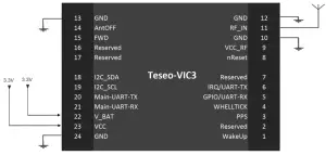
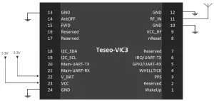
In Figure 1 the pin-out of the module:
Figure 1. Teseo-VIC3 pinout
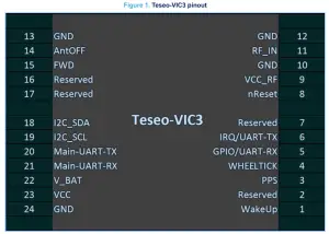
In Table 2 the pin-out description.
Table 2. Teseo-VIC3 pin out description
| Number | Name | I/O | Description |
| 1 | WakeUp | I | External interrupt pin (if not used, must be left floating) |
| 2 | Reserved | – | Reserved |
| 3 | PPS | O | Time pulse (PPS) |
| 4 | WHELLTICK | I | DRAW wheel tick signal |
| 5 | Reserved | – | NC |
| 6 | IRAQ | O | IRQ (if not used, must be left floating) |
| 7 | Reserved | – | NC |
| 8 | reset | I | The input signal to force the module under reset |
| 9 | VCC_RF | O | Output voltage RF section. It can be used to supply external active antenna |
| 10 | GND | Ground | Ground |
| 11 | RF_IN | I | RF input signal |
| 12 | GND | Ground | Ground |
| 13 | GND | Ground | Ground |
| 14 | Ant_OFF | O | External antenna control set level pull-up or pull-down to ensure proper standby current; |
| 15 | FWD | I | These-DRAW forward signal (if not used, must be left floating) |
| 16 | Reserved | – | Reserved |
| 17 | Reserved | – | Reserved |
| 18 | I2C_SDA | I/O | I2C-Data (internal 10 k pull-up) |
| 19 | I2C_SDL | I/O | I2C-Clock (internal 10 k pull-up) |
| 20 | UART-TX | O | UART-TX |
| 21 | UART-RX | I | UART-RX |
| 22 | V_BAT | I | Backup voltage supply |
| 23 | VCC | I | Supply voltage |
| 24 | GND | Ground | Ground |
Power
Teseo-VIC3 is supplied by two power pins: VCC (pin 23), and VBAT (pin 22).
2.1 VCC (pin#23)
VCC is the main supply.
VCC has to be 3.3 V ± 10%.
At startup or during low power application current can change suddenly. It is important that supply IC can provide current consumption of 130 mA.
2.2 VBAT (pin#22)
VBAT is the supply for the low-power domain backup: backup RAM and RTC.
VBAT can be either connected to VCC or it can be supplied by a dedicated supply always ON. When VBAT supply is kept ON VBAT must be 3.3 V ± 10%.
2.3 GND (pin#10, #12, #13, #24)
In Teseo-VIC3 pin#10, pin#12, pin#13 and pin#24 are ground reference.
Figure 2 shows the minimum connection to make Teseo-VIC3 GNSS work.
Figure 2. Teseo-VIC3 minimum connection
Reserved (pin#2, #5, #7, #16, #17)
In Teseo-VIC3 pin#2, pin#5, pin#7, pin#16, and pin#17 are reserved.
Interfaces
4.1 I2C (pin#18, #19)
I2C port is only compatible with 3.3 V IO voltage.
Teseo-VIC3 acts on the I2C-bus as slave only.
An internal 10 k pull-up resistor on the VCC is present. It is important to avoid having another pull-up for current leakage in low power mode.
4.2 UART (pin#20, #21)
UART is a universal asynchronous receiver/transmitter that supports much of the functionality of the industry-standard 16C650 UART.
This UART differs from the industry-standard 16C650 on some minor points which are:
- Receive FIFO trigger levels
- The internal register map address space, and the bit function of each register differ
- The deltas of the modem status signals are not available
- 1.5 stop bits are not supported
- The Independent receive clock feature is not supported
For the first PCB, it is recommended to plan to have some filtering components on Teseo-VIC3 UART lines.
I/O pins
5.1 PPS (pin#3)
PPS is the time pulse per second. It can be configured with the different conditions of pulses.
For the first PCB, it is recommended to plan to have some filtering components on the Teseo-VIC3 PPS pin.
5.2 WakeUp (pin#1)
It is an external interrupt that is used to wake up Teseo-VIC3 for asynchronous wake-up during standby software for instance.
The wake-Up pin is active high.
It can be activated by a GPIO from the host for instance.
5.3 reset (pin#8)
It forces the Tese-VIC3 under reset.
The reset signal is active low.
Host processors must have full control of this pin to guarantee the Teseo-VIC3’s firmware upgrade support.
5.4 RF_IN (pin#11)
It is the RF input.
No DC is present.
ESD diode is present. Avoid any DC on the pin.
5.5 off (pin#14)
AntOFF is a GPIO used to switch OFF external LNA or switch OFF current for the active antenna.
5.6 IRQ (pin#5)
It is a GPIO-Out signal driver by Teseo-VIC3 to notify the host of an internal event that happened.
IRQ pin is active high.
This pin must be tightened too high or low (pull-up or pull-down) in case standby state will be used
DRAW pins
Teseo-VIC3DA has two special pins to acquire odometer information:
• FWD pin#15
• WHEELTICK pin#4
6.1 FWD (pin#15)
FWD is an input pin-compatible to 3.3V IO voltage.
It reports the movement’s direction.
In details:
• A logical high value means forwards direction
• A logical low value means the backward direction
A 10 k pull-up or pull-down is necessary in case of software standby usage.
6.2 WHEELTICK (pin#4)
WHEELTICK is an input pin-compatible to 3.3V IO voltage.
It‘s a pulsing signal which reports the wheel movement.
The number of pulses per wheel revolution has to be configured in the firmware (CDB-ID 653).
Standby modes
Standby mode is the mode where only a low power backup domain is running. It means VBAT must be always maintained. It allows having very low current consumption and fast GNSS reacquisition at the end of the standby time due to RTC.
Teseo-VIC3 offers two different ways of standby:
• Software standby
• VCC standby
As IO buffers are not supplied during standby mode, it is important to keep all IO without external voltage to avoid any current leakage. UART_RX is an exception it can be left high.
Software standby
Software standby is activated by the binary for periodic standby. More details on how to set it are in the Software
Manual. As HW standby, all supplies are kept ON.
Periodic fixes are from 5 s up to 24 hours between 2 fixes.
It ensures a current below 30 µA (20 µA type.) on Teseo-VIC3.
Be careful that VCC_RF is ON during this standby, then in the case of the active antenna, it is important to switch them OFF.
VCC standby
VCC standby is ensured by switching OFF the VCC supply. It can be activated asynchronously from the GNSS binary with one GPIO switching OFF the supplies from a host.
During this standby, only VBAT is kept ON.
It ensures a current below 15 µA (TBC). During this standby mode, VCC_RF is OFF.
Front ends management
RF input impedance is 50 Ω.
8.1 Passive antenna
A passive antenna can be directly connected to Teseo-VIC3.
In addition, it could be possible that a matching component must be necessary to match the antenna.
Figure 3. Connection with passive antenna
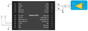
8.2 Active antenna
In the case of an active antenna, the antenna power supply can be acquired from VCC_RF (pin#9) which is a filtered mirror of VCC.
Figure 4. Teseo-VIC3 with Active Antenna
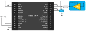
Moreover, to optimize the current during low power operating mode, the active antenna can be used with a switch to cut the current flow during the standby operation.
To achieve that the ANT_OFF (pin#14) signal can be used as enable on an external switch as shown in Figure 5.
Figure 5. Teseo-VIC3 with active antenna and switch control
Reference schematic and BOM
Schematics
Figure 6. VIC application schematic
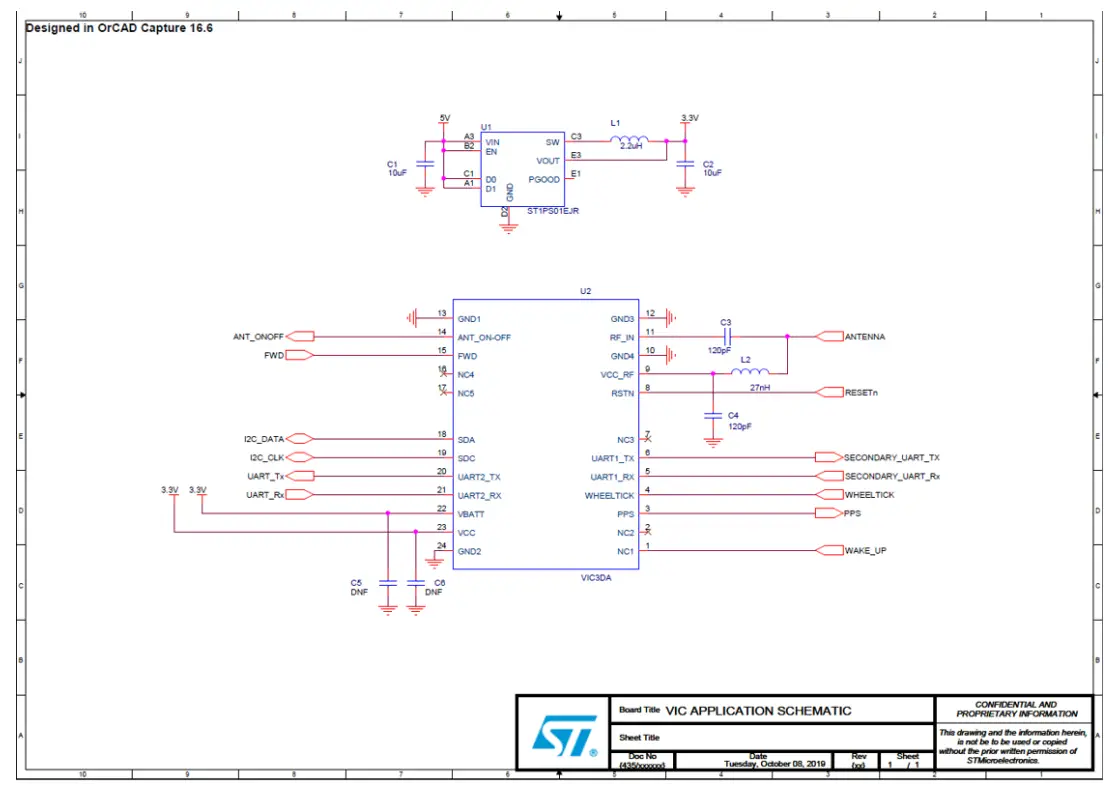
| Ref. | Value | Description | Manufacturer code | |
| Name | Part number | |||
| C1,C2 | 10 µF | Chip multilayer ceramic capacitors for general purpose 10 uF+/-20% 0603 X5R 16Vdc | Murata | GRM188R61C106MA73 |
| C3,C4 | 120 µF | Automotive-grade surface mount 0402 capacitor ceramic 120PF, 5% 50 V C0G | Murata | GCM1555C1H121JA16 |
| C5, C6 | NA | 0603 capacitor footprint in case of filtering needed | Murata | GCM1555C1H121JA16 |
| L1 | 2.2 µH | Surface mount multilayer type inductor for power line 2.2 µH | Murata | LQM21PN2R2MGH |
| L2 | 27 NH | Surface mount inductor inductance: 27 NH ±5% | Murata | LQG15HS27NJ02 |
| U1 | 400 mA nano-quiescent synchronous step-down converter with digital voltage selection and power good | STMicroelectronics | ST1PS01EJR | |
| U2 | Dead reckoning global navigation satellite system (GNSS) Teseo-VIC3 module | STMicroelectronics | Teseo-VIC3x | |
Layout recommendations
The RF input pin RF_IN (pin#11) is DC-cut.
For RF passive components, ST recommends using the 0402 (1×0.5mm) components. Please choose the RF ground-layer to be able to get 50 ohms RF line width as close as possible to components pads to avoid impedance offsets.
Antenna recommendations
Patch antennas
They have the advantage to be cheap, with good efficiency and highly directive. They can be used when mounted on a horizontal support.
For efficiency, the bigger are the antennas and the better are the performance.
The following table gives some antenna compatible part numbers.
Table 4. List of antenna p/n
| Manufacturer | Part number | Constellation | Size |
| Taoglas | CGGBP.25.4.A.02 | GPS+Glonass+Beidou | 25 × 25 mm |
| Taoglas | CGGBP.25.2.A.02 | GPS+Glonass+Beidou | 25 × 25 mm |
| Taoglas | CGGP.18.4.C.02 | GPS+Glonass | 18 × 18 mm |
| Yageo | ANT2525B00DT1516S | GPS+Glonass | 18 × 18 mm |
| Yageo | ANT1818B00CT1575S | GPS+Glonass | 25 × 25 mm |
The following table gives some SMD patch antenna part numbers compatible with GPS+Glonass:
Table 5. List of SMD antenna
| Manufacturer | Part number | Constellation | Size |
| Taoglas | SGGP.25.4.A.02 | GPS+Glonass | 25 × 25 mm |
| Taoglas | SGGP.18.4.A.02 | GPS+Glonass | 18 × 18 mm |
| Yageo | ANT1818B00BT1516S | GPS+Glonass | 18 × 18 mm |
| Yageo | ANT2525B00BT1516S | GPS+Glonass | 25 × 25 mm |
On the antenna side, there is only a ground plane as large as the antenna with one big via for the antenna pin. If the ground plane can be larger than the antenna side, it will improve the antenna performance. The antenna is usually glued and soldered with the pin.
Chip antenna
Chip antennas have the advantage to be small. They are less directive than the patch antennas with spherical radiation. Most of the time PCB must be empty of copper. Below the antenna position with a certain aperture.
Table 6. List of the chip antenna
| Manufacturer | Part number | Constellation | Size |
| Taoglas | GGBLA.01.A | GPS+Glonass+Beidou | 3.2×1.6 mm |
| Ethertronics | M830120 | GPS+Glonass+Beidou | 8×3 mm |
Remote antenna
Remote antenna means an antenna connected to PCB where Teseo-VIC3 is soldered with an RF connector.
Revision history
Table 7. Document revision history
| Date | Version | Changes |
| 17-Feb-2021 | 1 | Initial release. |
IMPORTANT NOTICE – PLEASE READ CAREFULLY
STMicroelectronics NV and its subsidiaries (“ST”) reserve the right to make changes, corrections, enhancements, modifications, and improvements to ST products and/or to this document at any time without notice. Purchasers should obtain the latest relevant information on ST products before placing orders. ST products are sold pursuant to ST’s terms and conditions of sale in place at the time of order acknowledgment.
Purchasers are solely responsible for the choice, selection, and use of ST products and ST assumes no liability for application assistance or the design of Purchasers’ products.
No license, express or implied, to any intellectual property right is granted by ST herein.
Resale of ST products with provisions different from the information set forth herein shall void any warranty granted by ST for such product.
ST and the ST logo are trademarks of ST. For additional information about ST trademarks, please refer to www.st.com/trademarks. All other product or service names are the property of their respective owners.
Information in this document supersedes and replaces information previously supplied in any prior versions of this document.
© 2021 STMicroelectronics – All rights reserved


