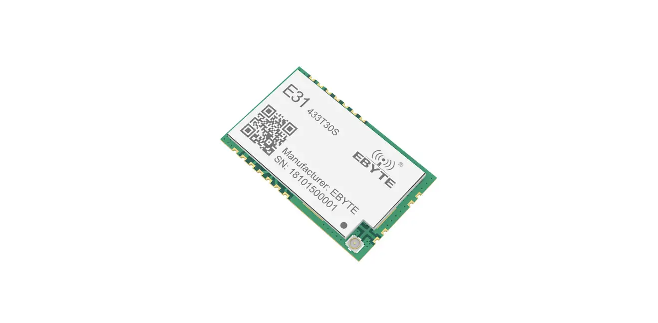
![]() E31-433T30S AX5243 433MHz 1W SMD Wireless Module
E31-433T30S AX5243 433MHz 1W SMD Wireless Module
User Manual
Disclaimer
EBYTE reserves all rights to this document and the information contained herein. Products, names, logos, and designs described herein may in whole or in part be subject to intellectual property rights. Reproduction, use, modification, or disclosure to third parties of this document or any part thereof without the express permission of EBYTE is strictly prohibited.
The information contained herein is provided “as is” and EBYTE assumes no liability for the use of the information. No warranty, either express or implied, is given, including but not limited, with respect to the accuracy, correctness, reliability, and fitness for a particular purpose of the information. This document may be revised by EBYTE at any time. For most recent documents, visit www.ebyte.com.
Overview
Introduction
 E31-433T30S is a 433M SMD type wireless serial port module (DART) imported from Switzerland AXSEM AX5243 RF chip, half-duplex, transceiver integrated, transparent transmission mode, 425-450.5MHz frequency band (default 433MHz), TTL level output with air wake-up function (ultra-low power consumption).
The module has a software FEC feature, which has high coding efficiency and strong error correction capability. In the case of sudden interference, it can actively correct the interfered data packets, greatly improving reliability and transmission distance. In the absence of FEC, such packets can only be discarded. The module has data encryption and compression capabilities. The data transmitted by the module in the air is random, and the data interception is meaningless through strict encryption and decryption algorithms. The data compression function has the probability of reducing the transmission time, reducing the probability of interference, improving reliability and transmission efficiency.
E31-433T30S strictly abides by FCC, CE, CCC and other domestic and foreign design specifications meets all RF-related certifications and meets export requirements.
Feature
- The tested communication range is 6km;
- The maximum transmission power is 30dBm (1W), and the software is multi-level settings;
- Supporting the global license-free ISM 433MHz band;
- Supporting data transmission rate from 1.2kbps to 70kbps;
- Supporting low power consumption, suitable for battery applications;
- Supporting 3.3V-4.5V power supply, 5V is recommended;
- Industrial class standard design, supporting for long-term use from -40 to 85°C;
- Supporting stamp hole and IPEX interface, users can choose to use according to their own needs.
Application scenario
- Home security alarm and remote keyless entry;
- Smart home and industrial sensors;
- Wireless alarm security system;
- Building automation solutions;
- Wireless industrial-grade remote control;
- Intelligent agriculture and oilfield solutions;
- Health care products:
- Advanced meter reading architecture framework;
- Automotive industry applications.
Specifications
Limit parameter
| Parameter | Item | Remark | |
| Min | Max | ||
| Power supply (V) | 0 | 6. | Voltage over 5.5V will cause permanent damage to the module |
| Blocking power (dBm) | . | 10 | Chances of burn are slim when modules are used in short distance |
| Operating temperature (°C) | -40 | 85 | / |
Parameter
| Parameter | Item | Remark | |||
| Min. | 1 p. | Max. | |||
| Operating voltage (V) | 3.3 | 5.0 | 5.5 | ≥5.0V ensures output power | |
| Communication level (V) | 3.3 | For 5V ITL, it may be at risk of burning down | |||
| Operating temperature (°C) | -40 | 25 | 85 | Industrial design | |
| Operate ng frequency (MHz) | 425 | 433 | 451. | Support ISM band | |
| Power consumption | TX current (mA) | 580 | 600 | 650 | Instant power consumption |
| RX current (mA) | 22 | 22 | 22 | ||
| Sleep current (pA) | 2 | 2 | 2 | Software is shut down | |
| Max Tx Power (dBm) | 30. | 30 | 30.8 | ||
| Receiving sensitivity (dBm) | -123 | -123 | -123 | Air data rate is 1.2 kbps | |
| Air data rate (bps) | I.2k | 1.2k | 70k | Controlled via user’s programming | |
| Parameter | Description | Remark |
| Distance for reference | 6 km | Test condition: clear and open area, antenna gain: SdBi. antenna height: 2.5m, air data rate: 1.2kbps |
| TX length | 43 Byte | The maximum capacity of a single package is automatically subcontracted after it is exceeded. |
| Buffer | 512 Byte | |
| Modulation | GFSK | |
| Communication interface | TTL | @3.3V |
| Package | SMD | |
| Connector | 2.54mm | |
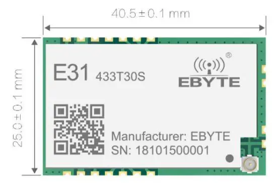
| Size | 40.5*25 mm | |
| Antenna | Stamp hole+IPEX | 5052 impedance |
Size and Pin definition
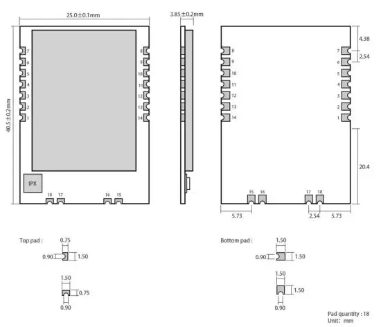
| No. | Pin | Direction | Description |
| I | MO | Input ( Weak pole pull ) | Work with M I to decide 4 working modes of the module (not suspended, if not used, could be grounded) |
| 2 | Ml | Input ( Weak pole pull ) | Work with MO to decide 4 working modes of the module (not suspended, if not used, could be grounded) |
| 3 | RDX | Input | TTL UART inputs, connect to external (MCU, PC) TXD output pin. Can be configured as open-drain or pull-up input |
| 4 | TXD | Input | TTL UART outputs, connect to external RDX (MCU, PC) input pin. Can be configured as open-drain or push-pull output |
| 5 | AUX | Output | To indicate the module’s working status & wake up the external MCU. During the procedure of self-check initialization, the pin outputs a low level. Can be configured as a push-pull output (suspending is allowed). |
| 6 | VCC | Power | Power supply: 3.3V — 5.5V DC |
| 7 | GND | Power | Ground |
| 8 | RESET | Input | Reset pin when the program is loaded (suspended, user wireless connection) |
| 9 | GND | Power | Power ground when the program is loaded (suspended, user wireless |
| connection) | |||
| 10 | SWIM | Input | SWIM pin when the program is loaded (suspended, user wireless connection) |
| 11 | +3.3V | Power | Power pin when the program is loaded (suspended, user wireless connection) |
| 12 | PD3 | I/O | NC pin, left floating, no connection required (for later expansion) |
| 13 | PD2 | I/O | NC pin, left floating, no connection required (for later expansion) |
| 14 | PD I | I/O | NC pin, left floating, no connection required (for later expansion) |
| 15 | GND | Power | Ground |
| 16 | GND | Power | Ground |
| 17 | GND | Power | Ground |
| 18 | ANT | Output | Antenna interface (high-frequency signal output. 5012 impedance) |
Connect to MCU
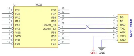
| No. | Description (STMSL MCU) |
| 1 | The UART module is TTL level. Please connect to the TTL level MCU. |
| 2 | Some 5V microcontrollers may require a 4-10K pull-up resistor on the TXD and AUX pins of the module. |
| Note: | The module communication level is 3.3V, please pay attention to the conversion of communication level when using a 5V microcontroller. |
Function description
Fixed transmission
Broadcasting transmission
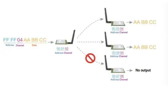
Broadcasting address
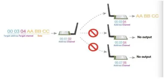
- For example: Set the address of module A as OxFFFF or Ox0000, and thc channel as 0x04;
- When the module is the transmitter (transparent transmission), all modules under channel Ox04 will receive the data, the purpose of broadcast is realized.
Monitor address
- For example: Set the address of module A as OxFFFF or Ox0000, and the channel as 0x04;
- When module A is the receiver, it can receive thc data sent from all modules under channel Ox04, the purpose of a monitor is realized.
Reset
- When the module is powered, AUX outputs low level immediately, conducts hardware self-check, and sets the operating mode based on user’s parameters. During the process, the AUX remains low level. After the process is completed, the AUX outputs high level and starts to work as per the operating mode combined by MI and MO. Therefore, users need to wait for the AUX rising edge as the start of the module’s normal work.
AUX description
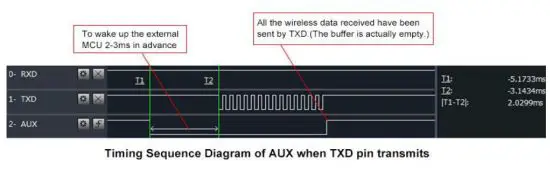
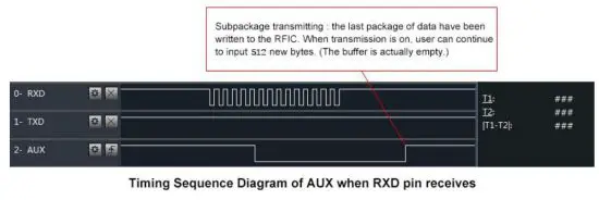
- AUX Pin can be used as an indication for wireless send & receive buffer and self-check.
- It can indicate whether there are data that are not sent yet via wireless way, whether all wireless data has been sent through UART, or whether the module is still in the process of self-check initialization.
Indication of UART output
- To wake up external MCU
Indication of wireless transmitting
- Buffer (empty): the internal 1000 bytes data in the buffer are written to the RFIC (Auto sub-packaging).
- When AUX=1, the user can input data less than 1000 bytes continuously without overflow. Buffer (not empty): when AUX4J, the internal 1000 bytes data in the buffer have not been written to the RFIC completely. If the user starts to transmit data at this circumstance, it may cause overtime when the module is waiting for the user data, or transmitting wireless subpackage.
- [ Note]: When AUX = 1, it does not mean that all the UART data of the module have been transmitted already, perhaps the last packet of data is still in transmission.
Configuration procedure of module
- Only happened when power-on resetting or exiting sleep mode

Notes for AUX
- For function 1 & function 2 mentioned above, the priority should be given to the one with low-level output, which means if it meets each of any low-level output conditions, AUX outputs a low level, if none of the low-level conditions is met, AUX outputs high level.
- When AUX outputs a low level, it means the module is busy & cannot conduct operating mode checking. Within LMS since AUX outputs a high level, the mode switch will be completed.
- After switching to the new operating mode, it will not work in the new mode immediately until AUX’s rising edge lasts for 2ms. If AUX stays on the high level, the operating mode switch can be effected immediately.
- When the user switches to other operating modes from mode 3 (sleep mode) or it’s still in the reset process, the module will reset user parameters, during which AUX outputs a low level.
Operating mode
- There are four operating modes, which are set by MI and MO, the details are as follows:
| Mode(0-3) | M1 | MO | Description | Remark |
| 0 Normal Mode | 0 | 0 | UART and wireless are enabled, transparent transmission is on | The receiver must be in mode 0.1 |
| I Wake-up mode | 1 | 0 | UART and wireless are enabled; The only difference from mode 0: the wake-up code is automatically added before the data packet is transmitted, so that the receiver working in mode 2 can be woken up. | The receiver can be in modes 0, 1, 2 |
| 2 Power saving mode | 0 | 1 | UART receive is turned off, the wireless is in awake mode, and after receiving the wireless data, UART is opened to send data. | The transmitter must be in mode 1 Cannot transmit data in this mode |
| 3 Sleep mode | 1 | 1 | The module goes to sleep and can receive parameter setting commands. | Refer to details below |
Mode switching
- Users can combine Ml and MO with high and low levels to determine the operating mode. Two GPIOs of the MCU can be used to control mode switching; After changing M 1 and MO: If the module is idle, after Ims, it can start working according to the new mode; If the serial port data of the module has not been transmitted through the wireless, the new working mode can be switched after the transmission is completed; If the module receives the wireless data and transmits the data through the serial port, it needs to finish transmission before switching the new working mode; Therefore, mode switching can only be valid when AUX output is 1, otherwise it will delay switching.
- For example, users continuously input a large amount of data and simultaneously perform mode switching. At this time, the switching mode operation is invalid; the module will process all the user data before performing the new mode detection; Therefore, the general recommendation is to detect the output state of the AUX pin and switch after 2ms when the output is high.
- When the module is switched from other modes to sleep mode, if the data has not been processed yet; The module will process these data (including receiving and sending) before entering sleep mode. This feature can be used for fast sleep, which saves power; for example, the transmitter module works in mode 0, the user transmits the serial port data “12345”, and then does not have to wait for the AUX pin to be idle (high level), and can directly switch to sleep mode. And the user’s main MCU immediately sleeps, the module will automatically transmit the user data through the wireless, and automatically enter sleep within 1 ms; This saves MCU’s working time and reduces power consumption.
- Similarly, any mode switching can use this feature. After the module processes the current mode event, it will automatically enter the new mode within I ms; thus eliminating the need for the user to query AUX and achieve the purpose of fast switching; For example, switching from the transmit mode to the receive mode; the user MCU can also enter sleep before the mode switch, and use the external interrupt function to acquire the AUX change, thereby performing mode switching.
- This operation mode is very flexible and efficient, is designed according to the user’s MCU’s operation convenience, and can reduce the workload of the entire system as much as possible, improve system efficiency, and reduce power consumption.
Normal mode ( Mode 0 )
| Type | MO=O, M1 = 0 |
| Transmitting | The module receives user data from the serial port. The module transmits a wireless data packet with a length of 58 bytes. When the user input data reaches 58 bytes, the module will initiate wireless transmission. At this time, the user can continue to input the data to be transmitted; when the data is less than 58 bytes, the module will wait for 3 bytes. If no user data continues to be input, the module considers the data to be terminated. At this time, the module transmits the data packet wirelessly; when the module receives the first user data, the AUX output is low. When the module inputs all the data into the RF chip and starts transmitting, the AUX output is high. At this time, it indicates that the last packet of wireless data has started to be transmitted, and the user can continue to input up to 512 bytes of data; the data packets transmitted by the module working in mode 0 can only be received by the receiving module working in mode 0, mode 1. |
| Receiving | The module always turns on the wireless receiving function and can receive the data packets transmitted from the modules which work in mode 0 and mode 1. After receiving the data packet, AUX will output a low level, and after delaying for 5rns, it will start to transmit wireless data through the serial port TXD pin. After all wireless data is output through the serial port, AUX will output high level. |
Wake-up mode (Mode 1)
| Type | MO = 1 , MI = 0 |
| Transmitting | The conditions for module start packet transmission and AUX function are the same as mode 0; the only difference is that the module will automatically add the wake-up code before each packet. The length of the wake-up code depends on the wake-up time set in the user parameter; The purpose of the wake-up code is to wake up the receiving module working in mode 2; therefore, the data transmitted by the module working in mode I can be received by the module working in mode 0, 1, 2. |
| Receiving | Equivalent to mode 0. |
Power saving mode (Mode 2)
| Type | MO = 0, M1 — 1 |
| Transmitting | The module is in the sleep state, the serial port is closed, and the serial port data from the external MCU |
| cannot be received, so this mode does not have the wireless transmission function. | |
| Receiving | In mode 2, the transmitter has to work in mode I; the wake-up code is monitored periodically, and once a valid wake-up code is received, the module will continue to receive and wait for the entire valid data packet to be received; then the AUX outputs low level. After delaying for 5ms, the module will open the serial port and send the received wireless data through TXD, then the AUX outputs high level; then the module continues to enter the “sleeping-monitoring” working state (polling); by setting different wake-up times. There are different receive response delays (up to 2s) and average power consumption (minimum 30uA); users need to strike a balance between communication delay and average power consumption. |
Sleep mode (Mode 3)
| Type | MO — 0, M1 — 1 |
| Transmitting | Unable to transmit data. |
| Receiving | Unable to receive data. |
| Configuration | It can be used for module parameter setting, using serial ports 9600 and 8N1, setting module parameters through specific commands. |
| Note | When entering the other modes from sleep mode, the module will reconfigure the parameters. During the configuration process, AUX will remain low; after the configuration is completed, AUX will output a high level, so it is recommended that the user detect the AUX rising edge. |
Command format
In sleep mode (mode 3: M0=1, M1=1), the list of supported commands is as follows (when setting, only 9600, 8N1 serial format is available):
| No. | Command | Description |
| I | CO+working parameters | The CO+5 bytes working parameter is sent in hexadecimal format, a total of 6 bytes, and must be sent continuously (power-off saved automatically) |
| 2 | Cl+Cl+CI | Three “Cl” are sent in hexadecimal format. The module returns the saved parameters and must be sent continuously. |
| 3 | C2+working parameters | The C0+5 bytes working parameter is sent in hexadecimal format, a total of 6 bytes, and must be sent continuously (power-off not saved) |
| 4 | C3+C3+C3 | Three “C3” are sent in hexadecimal format. The module returns the version information and must be sent continuously. |
| 5 | C4+C4+C4 | Three “C4” are sent in hexadecimal format, and the module will reset and must be sent continuously. |
Factory default parameter
| Factory default parameter: CO 00 00 18 50 44 | |||||||
| Model | Frequency | Address | Channel | Air data rate | Baud rate | Calibration | TX power |
| E31-433T30S | 433MHz | Ox0000 | 0x50 | 1.2kbps | 9600 | 8141 | 1W |
Working parameter reading
| Command format | Description |
| Cl+Cl+CI | In sleep mode (M@l, M1=1), a command (HEX format) is sent to the module serial port: Cl CI Cl, the module will return the current configuration parameters, such as CO 00 00 IA 17 44. |
Version information
| Command format | Description |
| C34C3+C3 | In sleep mode (MO= I. MI =1). a command is sent to the module serial port (HEX format): C3 C3 C3. the module will return the current configuration parameters. such as: C3 31 xx yy; the second byte represents the frequency. if it is 31. it is the applicable frequency of 433MHz; if it is 51. it is the applicable frequency of 230MHz; xx is the version number, and yy refers to other characteristics of the module. |
Reset
| Command format | Description |
| C4-PC4-PC4 | In sleep mode (MI: I. M1=1). a command is sent to the module serial port (HEX format): C4 C4 C4. the module will reset; during reset, the module performs a self-test. AUX will output a low level, after the reset. AUX will output a high level. and the module gait to work normally. At this time, you can switch modes or send the next command. |
Parameter setting command
| No. | Item | Description | Remark | |||
| 0 | HEAD | Fixed OxCO or OxC2, indicates that this data is a control command | Must be OxCO or OxC2 CO: The parameters will be saved after power off. C2: The parameters will not be saved after power off. | |||
| I | ADDH | Module address high byte (default OOH) | 00H-FFH | |||
| 2 | ADDL | Module address low byte (default OOH) | 00H-FFH | |||
| 3 | SPED | 7 | 6 | Serial parity byte | The serial port mode of the two communication parties can be different | |
| 0 | 0 | 8NI ( default ) | ||||
| 0 | I | 801 | ||||
| I | 0 | 8 El | ||||
| I | I | 8NI ( Equivalent to 00 ) | ||||
| 5 | 4 | 3 | TTL serial port rate ( bps ) | The baud rate of the two communication parties can be different The baud rate is independent of the wireless transmission parameters and does not affect the wireless transmission | ||
| 0 | 0 | 0 | Baud rate 1200 | |||
| 0 | 0 | I | Baud rate 2400 | |||
| 0 | I | 0 | Baud rate 4800 | |||
| 0 | I | I | Baud rate 9600 (default) | |||
| I | 0 | 0 | Baud rate 19200 | |||
| I | 0 | I | Baud rate 38400 | and reception characteristics. | ||
| 1 | I | 0 | Baud rate 57600 | |||
| I | 1 | I | Baud rate 115200 | |||
| I | 0 | Air data rate (bps) | The lower the air data rate. the farther the | |||
| 0 | 0 | 0 | Air data rate I.2k, default ) | range. the stronger the anti-interference performance and the longer the transmission time. The air data rate of both communication parties must be the same. | ||
| 0 | 0 | I | Air data rate 2.4k | |||
| 0 | I | 0 | Air data rate 4.8k | |||
| 0 | I | 1 | Air data rate 9.6k | |||
| I | 0 | 0 | Air data rate 19.2k | |||
| I | 0 | I | Air data rate 38.4k | |||
| 1 | I | 0 | Air data rate 50k | |||
| I | I | I | Air data rate 70k | |||
| 4 | CHAN | 7 | 6 | 5 | Reserved unused | Write 0. |
| Channel | 450.5MHz | |||||
| 00H-FFH. Corresponding to 425 -4-0Corresponding to, 4-5M – CHAN • 0.1 ht J . default 5011 433M ) | ||||||
| 5 | OPTION | 7 | Fixed transmission mode enable bit ( like MODBUS ) | When it is I. the first 3 bytes of data are the high address, the low address, and the channel. When transmitting. the module changes its own address and channel, and when it is finished. it restores the original settings. | ||
| 0 | Transparent transmission mode | |||||
| 1 | Fixed transmission mode | |||||
| 6 | 10 Drive mode ( default I) | This bit is used to enable the internal pull-up resistor of the module. Open-drain mode is more adaptable. and in some cases, an external pull-up resistor may be required. | ||||
| 1 | TXD. AUX push-pull. RDX pull up the input | |||||
| 0 | TXD. AUX open output. RDX open input | |||||
| 5 | 4 | 3 | Wireless wake uptime | Both the receiving and transmitting modules work in mode 0. The delay time is invalid and can be of any value. The transmitter works in mode I. and will continue to transmit the wake-up code for the corresponding time. The receiver works in mode 2, this time refers to the receives monitoring interval (wireless wake-up), and can only receive the data of the transmitting party working in mode I. | ||
| 0 | 0 | 0 | 2SOms *default ; | |||
| 0 | 0 | 1 | 500ms | |||
| 0 | I | 0 | 750ms | |||
| 0 | I | 1 | 1000ms | |||
| I | 0 | 0 | 1250ms | |||
| I | 0 | I | 1500ms | |||
| I | I | 0 | 1750ms | |||
| I | I | I | 2000ms | |||
| 2 | FEC | After the FEC is turned off, the actual data transmission rate is increased, but the anti-interference performance is weakened and the distance is closer. Please choose to turn on or off according to the actual application. Both sides of the communication must be turned on or off at the same time. | ||||
| 0 | Turn off FEC | |||||
| I | Turn on FEC ( default ) | |||||
| 1 | 0 | I TX power | The external power supply must provide | |||
| 0 | 0 | 30dBm ( default) | more than 1.5A current output capability. And ensure that the power supply ripple is less than 100mV. It is not recommended to use a smaller power transmission, and the power utilization efficiency is not high. | |||||||||
| 0 | I | 27dBm | ||||||||||
| I | 0 | 24dBm | ||||||||||
| 1 | I | 21dBm | ||||||||||
| Example (The meaning of the No. 3 “SPED” byte) | ||||||||||||
| Binary bit | 7 | 6 | 5 | 4 | ; | I | 0 | |||||
| Specific value (user configuration) | 0 | 0 | 0 | 1 | I | 0 | I | 0 | ||||
| Representative meaning | Serial parity bit 8N1 | Baud rate 9600 | Air data rate 2.4k | |||||||||
| Corresponding hexadecimal bit | I | A | ||||||||||
Hardware design
- It is recommended to use a DC stabilized power supply. The power supply ripple factor is as small as possible, and the module needs to be reliably grounded.;
- Please pay attention to the correct connection of the positive and negative poles of the power supply. The reverse connection may cause permanent damage to the module:
- Please check the power supply to ensure it is within the recommended voltage otherwise when it exceeds the maximum value the module will be permanently damaged;
- Please check the stability of the power supply, the voltage can not fluctuate frequently;
- When designing the power supply circuit for the module, it is often recommended to reserve more than 30% of the margin, so the whole machine is beneficial for long-term stable operation.;
- The module should be as far away as possible from the power supply, transformers, high-frequency wiring, and other parts with large electromagnetic interference.:
- High-frequency digital muting, high-frequency analog routing, and power routing must be avoided under the module. If it is necessary to pass through the module, assume that the module is soldered to the Top Layer, and the copper is spread on the Top Layer of the module contact part(well-grounded), it must be close to the digital part of the module and muted in the Bottom Layer;
- Assuming the module is soldered or placed over the Top Layer, it is wrong to randomly route over the Bottom Layer or other layers, which will affect the module’s spurs and receiving sensitivity to varying degrees:
- It is assumed that there are devices with large electromagnetic interference around the module that will greatly affect the performance. It is recommended to keep them away from the module according to the strength of the interference. If necessary, appropriate isolation and shielding can be done;
- Assume that there are traces with large electromagnetic interference (high-frequency digital, high-frequency analog, power traces) around the module that will greatly affect the performance of the module. It is recommended to stay away from the module according to the strength of the interference. If necessary, appropriate isolation and shielding can be done:
- If the communication line uses a 5V level, an elk-5.1k resistor must be connected in series (not recommended, there is still a risk of damage);
- Try to stay away from some physical layers such as TTL protocol at 2AGHz, for example, USB3.0:
- The mounting structure of the antenna has a great influence on the performance of the module. It is necessary to ensure that the antenna is exposed, preferably vertically upward. When the module is mounted inside the case, use a good antenna extension cable to extend the antenna to the outside:
- The antenna must not be installed inside the metal case, which will cause the transmission distance to be greatly weakened.
FAQ
The communication range is too short
- The communication distance will be affected when an obstacle exists.
- Data loss rate will be affected by temperature, humidity, and co-channel interference.
- The ground will absorb and reflect winless radio waves, so the performance will be poor when testing near the ground.
- Seawater has a great ability in absorbing wireless radio waves, so performance will be poor when testing near the sea.
- The signal will be affected when the antenna is near a metal object or put in a metal case.
- The power register was set incorrectly, the air data rate is set as too high (the higher the air data rate, the shorter the distance).
- The power supply low voltage under room temperature is lower than 2.5V, the lower the voltage, the lower the transmitting power.
- Due to antenna quality or poor matching between antenna and module.
The module is easy to damage
- Please check the power supply source, ensure it is 2.0V-3.6V, voltage higher than 3.6V will damage the module.
- Please check the stability of the power source, the voltage cannot fluctuate too much.
- Please make sure antistatic measures are taken when installing and using, high-frequency devices that have electrostatic susceptibility.
- Please ensure the humidity is within a limited range, some parts are sensitive to humidity.
- Please avoid using modules under too high or too low temperatures.
BER(Bit Error Rate) is high
- There are co-channel signal interference nearby, please be away from interference sources or modify frequency and channel to avoid interference;
- The poor power supply may cause messy code. Make sure that the power supply is reliable.
- The extension line and feeder quality are poor or too long, so the bit error rate is high;
Production guidance
Reflow soldering temperature
| Profile Feature | Curve characteristics | Sn-Pb Assembly | Pb-Free Assembly |
| Solder Paste | Solder paste | Sn63/Pb37 | Sn96.5/Ag3/Cu0.5 |
| Preheat Temperature min (Tasmin) | Min preheating temp. | 100°C | 150°C |
| Preheat temperature max (Tmax) | Mx preheating temp. | 150°C | 200°C |
| Preheat Time (Tasmin to Tsmax)(ts) | Preheating time | 60-120 sec | 60-120 sec |
| Average ramp-up rate(Ts max to Tp) | Average ramp-up rate | 3°C/second max | 3°C/second max |
| Liquidous Temperature (TL) | Liquid phase temp. | 183°C | 217°C |
| Time (to) Maintained Above (TL) | Time below liquid phase line | 60-90 sec | 30-90 sec |
| Peak temperature (Tp) | Peak temp. | 220-235°C | 230-250°C |
| Average ramp-down rate (Tp to Tsmax) | Average ramp-down rate | 6°C/second max | 6°C/second max |
| Time 25°C to peak temperature | Time to peak temperature for 25°C | max 6 minutes | max 8 minutes |
Reflow soldering curve
 E31 Series
 E31 Series
| Model No. | Core IC | Frequency Hz | Tx power dBm | Distance km | Package | Size mm | Antenna | Model No. |
| E3 I -230T33D | AX5243 | 230M | 33 | 8 | I.2k-70k | DIP | 37 * 60 | SMA-K |
| E3I -230T270 | AX5243 | 230M | 27 | 5 | 1.2k-70k | DIP | 24 ‘ 43 | SMA-K |
| EI1-210T17D | AX5243 | 230M | 17 | 2 | 1.2k-70k | DIP | 21 * 36 | SMA-K |
| £31-4331330 | AX5243 | 433M | 33 | 8 | I.2k-70k | DIP | 37 * 60 | SMA-K |
| E3 I -433TIOD | AX5243 | 433M | 30 | 6 | 1.2k-70k | DIP | 24′ 43 | SMA-K |
| E3I -433T27D | AX5243 | 433M | 27 | 4 | 1.2k-70k | DIP | 24’43 | SMA-K |
| E3 I -433TI7D | AX5243 | 433M | 17 | 2. | I.2k-70k | DIP | 21 * 36 | SMA-K |
| £31-4331175 | AX5243 | 433M | 17 | 2 | I.2k-70k | SMD | 17 ‘ 30 | Stamp hole+IPEX |
| E3 1 -433T I 7S3 | AX5243 | 433M | 17 | 2 | 1.2k-70k | SMD | 16* 26 | Stamp hole+IPEX |
| £31-433T30S | AX5243 | 433M | 30 | 9. | I.2k-70k | SMD | 40.5*25 | Stamp hole+IPEX |
Antenna recommendation
The antenna is an important role in the communication process. A good antenna can largely improve the communication system. Therefore, we recommend some antennas for wireless modules with excellent performance and reasonable prices.
| Model No. | Type | Frequency Hz | Interface | Gain dBi | Height | Cable | Function feature |
| TX431-NP-4310 | Flexible PCB antenna | 433M | SMA-J | 2 | 43.8*9.5mm | – | Built-in flexible, FPC soft antenna |
| TX433-1W-5 | Rubber antenna | 433M | SMA-J | 2 | 50mm | – | Flexible &omnidirectional |
| TX433-JWG-7 | Rubber antenna | 433M | SMA-J | 2.5 | 75mm | – | Flexible &omnidirectional |
| TX433-JK-20 | Rubber antenna | 433M | SMA-J | 3 | 210mm | – | Flexible &omnidirectional |
| TX433-1K- I I | Rubber antenna | 433M | SMA-J | 2.5 | 110mm | – | Flexible &omnidirectional |
| TX433-XP-200 | Sucker antenna | 433M | SMA-J | 4 | 19cm | 200cm | Sucker antenna, High gain |
| TX433-XP-I00 | Sucker antenna | 433M | SMA-J | 3.5 | 18.5cm | 100cm | Sucker antenna, High gain |
| TX433-XPH-300 | Sucker antenna | 433M | SMA-J | 6 | 96.5cm | 300cm | Sucker antenna, High gain |
| TX433-JZG-6 | Rubber antenna | 433M | SMA-J | 2.5 | 52mm | – | Short straight &omnidirectional |
| TX433-JZ-5 | Rubber antenna | 433M | SMA-J | 2 | 52mm | – | Short straight &omnidirectional |
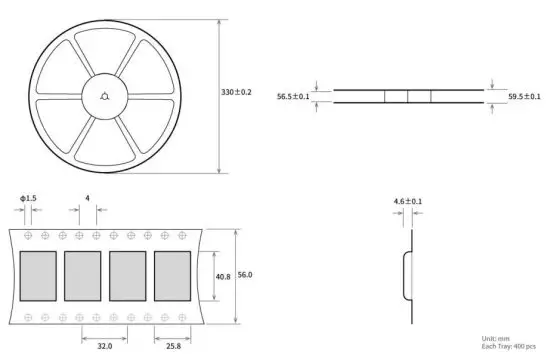
Package for batch order
Revision history
About us
Technical support: [email protected]
Documents and RF Setting download link: www.ebyte.com
Thank you for using Ebyte products! Please contact us with any questions or suggestions: [email protected]
Fax: 028-64146160 ext. 821
Web: www.ebyte.com
Address: Innovation Center D347, 4# XI-XIN Road, Chengdu, Sichuan, China![]()
Chengdu Ebyte Electronic Technology Co., Ltd.
Copyright ©2012-2019, Chengdu Ebyte Electronic Technology Co., Ltd.


