Microsemi UG0645 Low Voltage Differential Signaling
Product Information
The Microsemi LVDS 7:1 module is a hardware implementation of the low-voltage differential signaling (LVDS) interface standard. LVDS is a high-speed, low-power, general-purpose interface standard approved by the ANSI/TIA/EIA-644 standard in March 1996. The LVDS 7:1 module uses differential signaling with a nominal signal swing of 350 mV differential, which decreases rise and fall times to achieve the maximum transmission rates specified in the LVDS standard. With LVDS, signal swing does not depend on the voltage of any specific supply.
Hardware Implementation
The LVDS 7:1 module consists of a receive and transmit module. The receive module takes in data from up to seven sources and outputs it through a single LVDS line. The transmit module takes in data from a single source and outputs it to up to seven destinations through LVDS lines.
Inputs and Outputs
The LVDS 7:1 module has seven data inputs and one data output for the receive module, as well as one data input and seven data outputs for the transmit module. The module also has power and ground connections.
Timing Diagrams
The timing diagrams for the LVDS 7:1 module are provided in the user manual for reference. These diagrams show the timing requirements for input and output signals.
Loopback Test
A loopback test can be performed to verify the functionality of the LVDS 7:1 module. This test involves connecting the output of the transmit module to the input of the receive module, and checking that the output matches the input.
Performance Statistics
The user manual provides performance statistics for the LVDS 7:1 module, including data rate, signal swing, and power consumption.
Resource Utilization
The user manual also provides resource utilization information for the LVDS 7:1 module, including the number of logic elements and memory blocks used.
Product Usage
The LVDS 7:1 module can be used in a variety of applications that require high-speed data transmission between multiple sources and destinations. Prior to installation, carefully review the hardware implementation and timing diagrams provided in the user manual to ensure proper installation and functionality.
When connecting the module, ensure that power and ground connections are made correctly. The module should be connected to a power supply that meets the specifications provided in the user manual.
To test the functionality of the LVDS 7:1 module, perform a loopback test as described in the user manual. If any issues arise during testing or operation, refer to the troubleshooting section of the user manual or contact Microsemi customer support for assistance.
When designing a system that uses the LVDS 7:1 module, ensure that all timing requirements and other specifications are met. Consult with a product expert or engineer if necessary.
Microsemi makes no warranty, representation, or guarantee regarding the information contained herein or the suitability of its products and services for any particular purpose, nor does Microsemi assume any liability whatsoever arising out of the application or use of any product or circuit. The products sold hereunder and any other products sold by Microsemi have been subject to limited testing and should not be used in conjunction with mission-critical equipment or applications. Any performance specifications are believed to be reliable but are not verified, and Buyer must conduct and complete all performance and other testing of the products, alone and together with, or installed in, any end-products. Buyer shall not rely on any data and performance specifications or parameters provided by Microsemi. It is the Buyer’s responsibility to independently determine suitability of any products and to test and verify the same. The information provided by Microsemi hereunder is provided “as is, where is” and with all faults, and the entire risk associated with such information is entirely with the Buyer. Microsemi does not grant, explicitly or implicitly, to any party any patent rights, licenses, or any other IP rights, whether with regard to such information itself or anything described by such information. Information provided in this document is proprietary to Microsemi, and Microsemi reserves the right to make any changes to the information in this document or to any products and services at any time without notice.
About Microsemi
Microsemi Corporation (Nasdaq: MSCC) offers a comprehensive portfolio of semiconductor and system solutions for aerospace & defense, communications, data center and industrial markets. Products include high-performance and radiation-hardened analog mixed-signal integrated circuits, FPGAs, SoCs and ASICs; power management products; timing and synchronization devices and precise time solutions, setting the world’s standard for time; voice processing devices; RF solutions; discrete components; enterprise storage and communication solutions, security technologies and scalable anti-tamper products; Ethernet solutions; Power-over-Ethernet ICs and midspans; as well as custom design capabilities and services. Microsemi is headquartered in Aliso Viejo, California, and has approximately 4,800 employees globally. Learn more at www.microsemi.com.
Introduction
Low-voltage differential signaling (LVDS) is a high-speed, low-power, general-purpose interface standard. Also known as the ANSI/TIA/EIA-644 standard, LVDS was approved in March 1996. LVDS uses differential signaling with a nominal signal swing of 350 mV differential. The low signal swing decreases rise and fall times to achieve the maximum transmission rates specified in the LVDS standard. With LVDS, signal swing does not depend on the voltage of any specific supply.
LVDS uses current mode drivers, which limit power consumption. The differential signals are immune to ±1 V common voltage noise. The Channel-Link technology was originally developed as a solution for flat panel displays, using LVDS for the physical layer (PHY). The technology was then extended into a method for general purpose data transmission. Channel-Link consists of a driver pair and a receiver pair. The driver accepts 28 single-ended data signals and a single-ended clock. The data is 7:1 serialized, and four data streams and a dedicated clock are driven over five LVDS pairs. The receiver accepts all four LVDS data streams and the LVDS clock, and then drives the 28 bits of data and the clock to the board.
Microsemi LVDS 7:1 is a source-synchronous interface that consists of multiple data bits and a clock. The LVDS 7:1 solution consists of five LVDS pairs: four data pairs and a clock pair. It provides four independent, source-synchronous channels, and on each channel, one cycle of parallel clock includes seven bits of serialized data. The serial data on the four channels together translates to 28 bits parallel data. It is recommended that the pinouts and clocks of all the four data channels be placed in the same I/O bank. However, the pinouts can be assigned to different banks, provided the clocking requirements for the design are met.
The following figure shows the top-level block diagram of the four-channel LVDS 7:1 interface.
Figure 1 • LVDS 7:1 Top-Level Block Diagram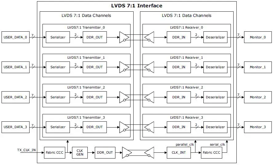
The LVDS 7:1 transmit and receive blocks perform the following:
- The transmit block uses double data rate registers to transmit data on both the rising and falling edges of the clock. It multiplies the parallel clock by 3.5 and uses the clock to transmit seven serial bits of data in one parallel clock cycle.
- The receive block uses double data rate registers to capture data on both the rising and falling edge of the clock. It multiplies the captured clock by 3.5 to generate the input for the DDR_IN macro.
Hardware Implementation
Design Description
This section provides information on the implementation of the LVDS 7:1 receive and transmit modules.
LVDS 7:1 Receive Module
The LVDS 7:1 receive module receives LVDS data and an LVDS clock from the FPGA’s high-speed LVDS buffers. The source-synchronous LVDS clock is passed to the fabric clock conditioning circuitry (CCC) block while the LVDS data is sent to the DDR_IN macro.
The fabric CCC block generates a serial clock (serial_clk) with a frequency of 3.5 times the input clock received from the transmitter (RX_CLK_IN).
The DDR_IN macro generates two streams of data at the rising edge of the serial clock. This data is then sent to the deserializer, which aligns the incoming data to a pre-defined training pattern. Once the data is aligned according to the word boundary defined in the training pattern, the align_serializer signal is enabled, and 14 bits of serialized data are sent to the RX_SYNC module. The RX_SYNC module synchronizes the 14-bit serial data to a parallel clock (parallel_clk), and then transmits a 7-bit parallel data as output.
The following block diagram shows the LVDS 7:1 receiver implementation, including input and output signals.
Figure 2 • LVDS 7:1 Receiver Block Diagram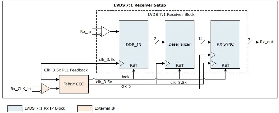
LVDS 7:1 Transmit Module
The LVDS 7:1 transmit module receives seven bits of parallel data and a parallel clock, TX_CLK_in. TX_CLK_in is sent to the fabric CCC block, which generates two output clocks: a parallel clock with the same frequency as TX_CLK_in, and a serial clock with a frequency 3.5x that of TX_CLK_in.
The TX SYNC module synchronizes the incoming seven bits of parallel data with the output clocks and transmits the synchronized data to the serializer block. The serializer block then serializes the seven bits of parallel data into two bits of serial data. These two bits of serial data are passed to the DDR_OUT macro, which operates at the serial clock’s frequency. The serialized output data of the DDR_OUT macro is then transmitted out of the device using high-speed LVDS buffers.
The following block diagram shows the LVDS 7:1 transmitter implementation, including input and output signals.
Figure 3 • LVDS 7:1 Transmitter Block Diagram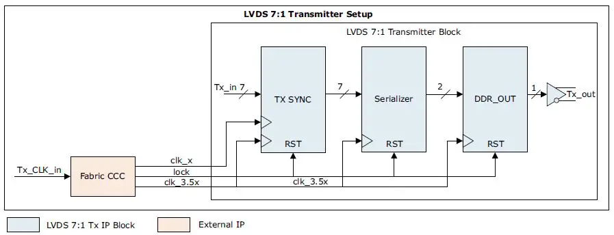
Inputs and Outputs
The following table lists the LVDS 7:1 receiver interface input and output ports.
Table 1 • LVDS 7:1 Receiver Interface Ports
| Signal Name | Direction | Width (in bits) | Description |
| Reset_n | Input | – | System reset |
| Serial_Clk | Input | – | System serial clock |
| parallel_clk | Input | – | Parallel clock |
| CAM_D3_P | Input | – | Serial input channel D rising |
| CAM_D3_N | Input | – | Serial input channel D falling |
| CAM_D2_P | Input | – | Serial input channel C rising |
| CAM_D2_N | Input | – | Serial input channel C falling |
| CAM_D1_P | Input | – | Serial input channel B rising |
| CAM_D1_N | Input | – | Serial input channel B falling |
| CAM_D0_P | Input | – | Serial input channel A rising |
| CAM_D0_N | Input | – | Serial input channel A falling |
| RDATA_A | Output | 7 | Parallel output data channel A |
| RDATA_B | Output | 7 | Parallel output data channel B |
| RDATA_C | Output | 7 | Parallel output data channel C |
| RDATA_D | Output | 7 | Parallel output data channel D |
| Align_serializer_a | Output | – | Channel A Rx alignment signal to the training pattern |
| Align_serializer_b | Output | – | Channel B Rx alignment signal to the training pattern |
| Align_serializer_c | Output | – | Channel C Rx alignment signal to the training pattern |
Table 1 • LVDS 7:1 Receiver Interface Ports
| Signal Name | Direction | Width (in bits) | Description |
| Align_serializer_d | Output | – | Channel D Rx alignment signal to the training pattern |
| Training pattern | Input | – | Pattern used to align Rx to Tx |
| CAM_CLKOUT_N | Input | – | Clock from fabric |
| CAM_CLKOUT_P | Input | – | Clock from fabric |
| Rclk_o | Input | – | LVDS receiver clock output |
The following table lists the LVDS 7:1 transmit interface input and output ports.
Table 2 • LVDS 7:1 Transmitter Interface Ports
| Signal Name | Direction | Width (in bits) | Description |
| RESET | Input | – | System reset |
| serial_clock | Input | – | System serial clock |
| parallel_clk | Input | – | Parallel clock |
| WDATA_A | Input | 7 | parallel data channel A |
| WDATA_B | Input | 7 | Parallel data channel B |
| WDATA_C | Input | 7 | Parallel data channel C |
| WDATA_D | Input | 7 | Parallel data channel D |
| PADP_TX_0 | Output | – | Serial channel A rising data |
| PADN_TX_0 | Output | – | Serial channel A falling data |
| PADP_TX_1 | Output | – | Serial channel B rising data |
| PADN_TX_1 | Output | – | Serial channel B falling data |
| PADP_TX_2 | Output | – | Serial channel C rising data |
| PADN_TX_2 | Output | – | Serial channel C falling data |
| PADP_TX_3 | Output | – | Serial channel D rising data |
| PADN_TX_3 | Output | – | Serial channel D falling data |
| PADN_CLK_OUT | Output | – | Output differential negative TX clock |
| PADP_CLK_OUT | Output | – | Output differential positive TX clock |
Timing Diagrams
The following figure shows the timing diagram for the LVDS 7:1 receiver.
Figure 4 • LVDS 7:1 Receiver Timing Diagram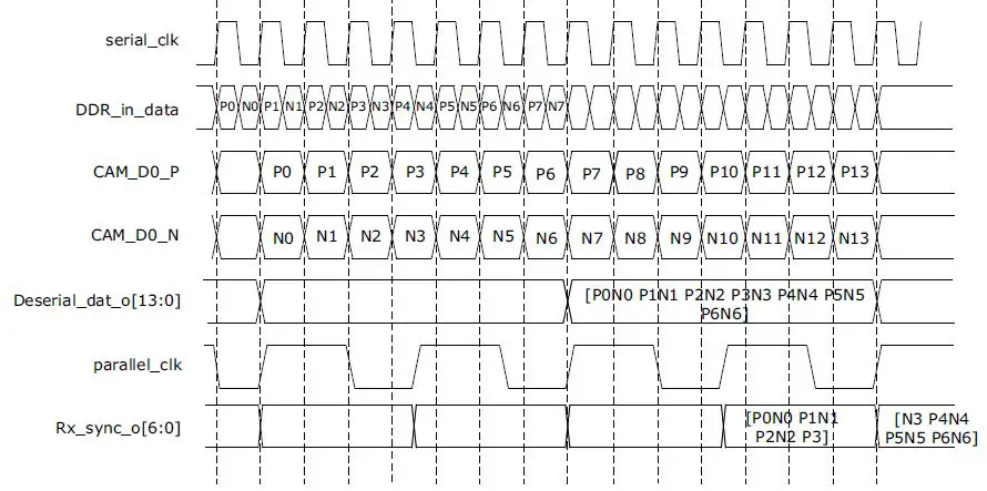
The following figure shows the timing diagram for the LVDS 7:1 transmitter.
Figure 5 • LVDS 7:1 Transmitter Timing Diagram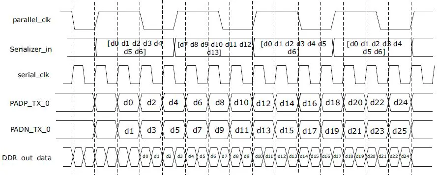
Loopback Test
A loopback test performed on the Microsemi SmartFusion2® M2S150 Advanced Development Kit to validate the LVDS 7:1 functionality. The test setup consisted of five parallel transmit and receive channels (four data channels and one clock channel), and the test was performed at varying speeds up to 90 MHz.
The M2S150 Advanced Development Kit provides an FMC high pin count (HPC) J64 connector interface. For the test, an LVDS QSE daughter card was installed on the HPC connector. This daughter card provides four Samtec QSE family connectors, which break out as a subset of the FMC HPC signal set.
The FMC HPC signals were connected as length-matched pairs to the QSE connectors. The pairs were then loop-backed using the Samtec loopback cable.
The following figure shows the test setup for the LVDS 7:1 loopback test.
Figure 6 • LVDS 7:1 Loopback Test Setup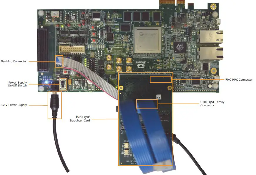
Performance Statistics
During the LVDS 7:1 interface design validation performed using M2S150 Advanced Development Kit, it was found that the LVDS 7:1 interface design successfully operated at a maximum frequency of 90 MHz for the parallel clock and 315 MHz for the serial clock with 3.5x the parallel clock’s frequency. Overall data transfer rates of up to 630 Mbps of data were achieved per LVDS pair. For more information about the test setup used for the validation, see Loopback Test, page 6.
Resource Utilization
The following table shows the resource utilization of a sample LVDS 7:1 block implemented in a SmartFusion2 M2S150T-1152FC device.
Table 3 • LVDS 7:1 Receiver Resource Utilization
| Resource | Usage |
| D flip-flops (DFF) | 990 |
| 4-input look-up tables (LUT) | 590 |
| Math blocks (MACC) | 0 |
| RAM1Kx18 | 0 |
| RAM64x18 | 4 |
Table 4 • LVDS 7:1 Transmitter Resource Utilization
| Resource | Usage |
| DFFs | 190 |
| 4-input LUTs | 80 |
| MACC | 0 |
| RAM1Kx18 | 0 |
| RAM64x18 | 0 |
Revision History
The revision history describes the changes that were implemented in the document. The changes are listed by revision, starting with the most current publication.
Revision 4.0
Updated the Figure 2, page 3.
Revision 3.0
The following is a summary of the changes in revision 3.0 of this document:
- Added the information about LVDS 7:1 loopback test For more information, see Loopback Test, page 6.
- Updated Performance statistics. For more information, see Performance Statistics, page 7.
- Updated Resource utilization details. For more information, see Resource Utilization, page 8.
Revision 2.0
Updated the SAR (76159).
Revision 1.0
The first publication of this document.
Microsemi Corporate Headquarters One Enterprise, Aliso Viejo,
CA 92656 USA
Within the USA: +1 (800) 713-4113 Outside the USA: +1 (949) 380-6100 Fax: +1 (949) 215-4996
Email: [email protected] www.microsemi.com
© 2016 Microsemi Corporation. All rights reserved. Microsemi and the Microsemi logo are trademarks of Microsemi Corporation. All other trademarks and service marks are the property of their respective owners.


