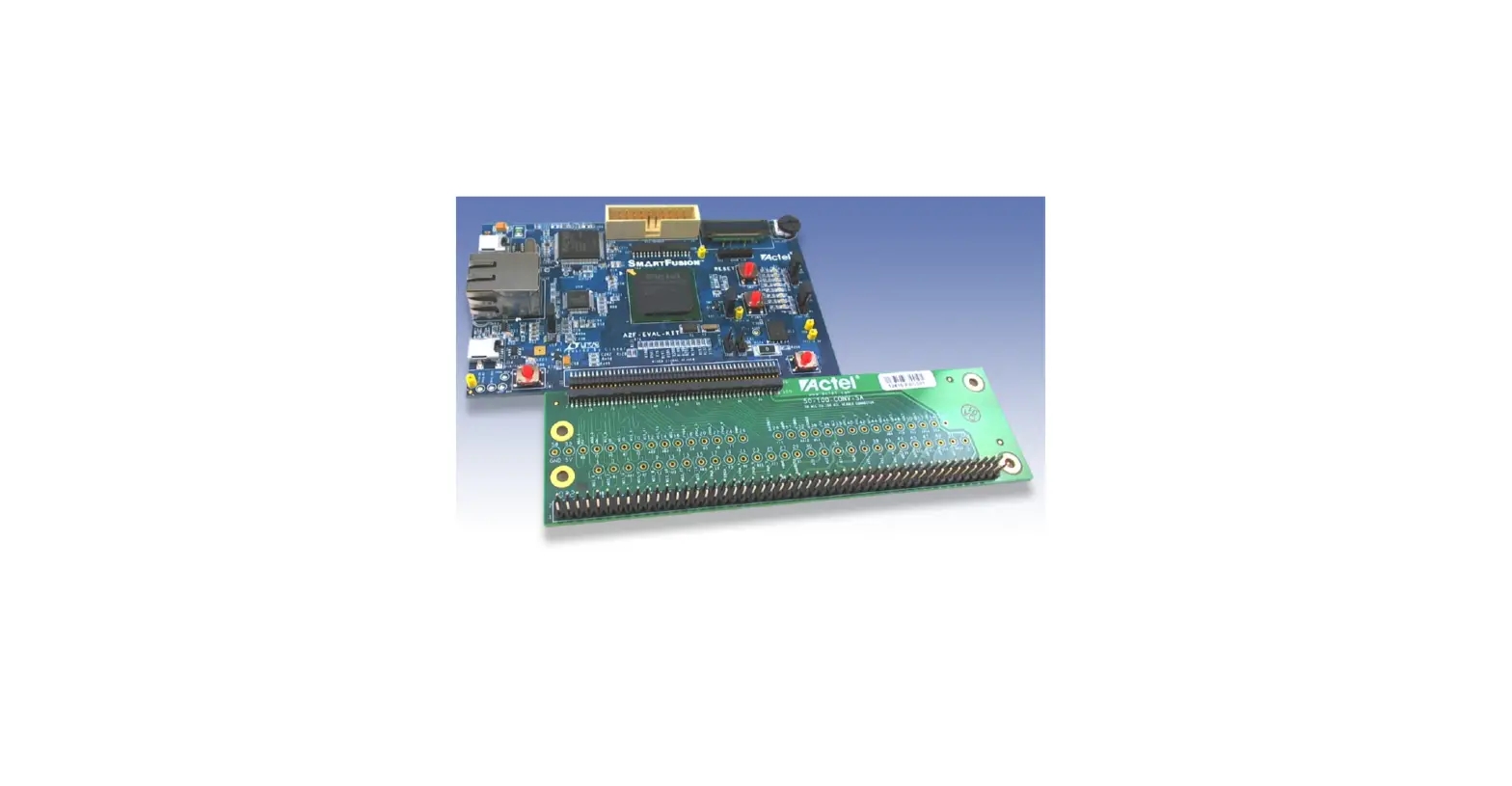
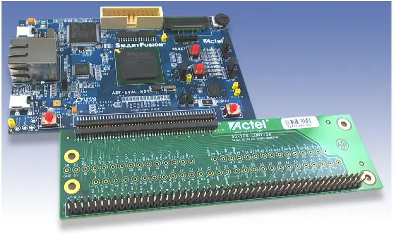
Microsemi Mixed Signal Daughter Card
Introduction
The Mixed Signal Daughter Card is designed for connection to the mixed signal header on the SmartFusion® Evaluation Kit (A2F-EVAL-KIT) or the SmartFusion Development Kit (A2F500-DEV-KIT). The board includes test points for the signals driven by the mixed signal header and also has a 100 mil header that can be used to wire wrap or solder signals directly. The board comes with rubber feet attached for use with the evaluation kit. If the board is being used with the development kit, the standoffs supplied in the box can be attached to match board height.
Features
The Mixed Signal Daughter Card features:
- Test points for signal probing
- Mixed signal header for daughter card support
- 100 mil header for wire-wrapped or soldered signals
Contents
The contents of the Mixed Signal Daughter Card are listed in Table 1.
| Quantity | Description |
| 1 | 50-100-CONV-SA mixed signal daughter card |
| 4 | 1/2″ plastic standoffs |
| 4 | Plastic screws (for 1/2″ plastic standoffs) |
Mixed Signal Connector
The mixed signal connector.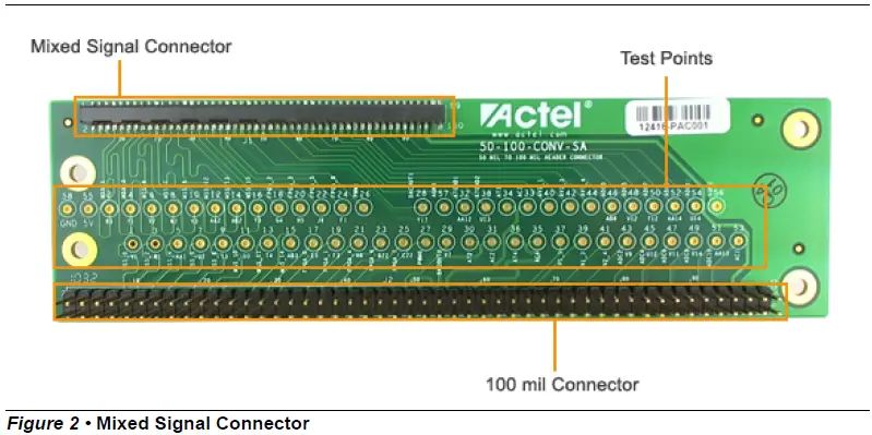
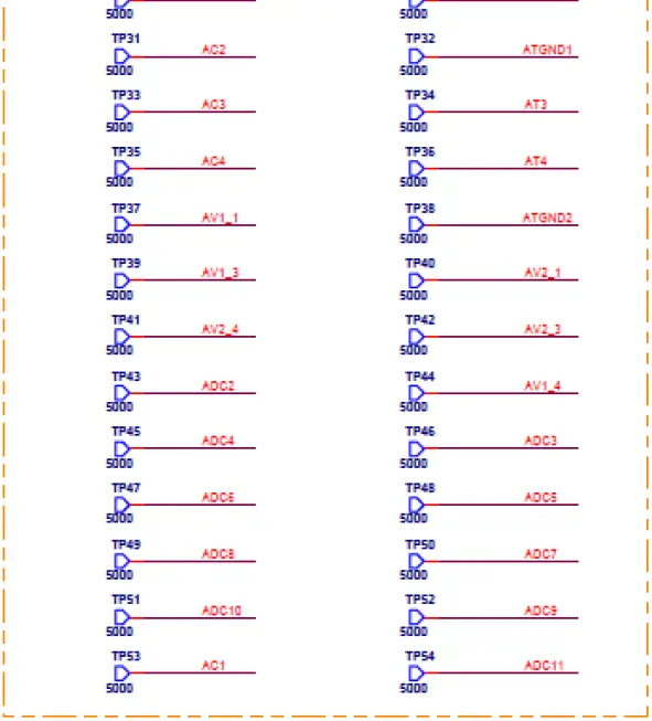
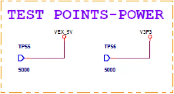
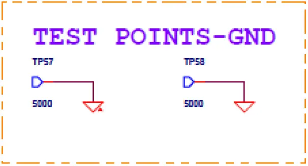
Test Points
Test Point Signals
The test point signals:
Test Point Signals for Mixed Signal Daughter Card 50-100-CONV-SA
| Test Points | Signal |
| TP1 | MSS_GP_IO_0 |
| TP2 | MSS_GP_IO_1 |
| TP3 | MSS_GP_IO_2 |
| TP4 | MSS_GP_IO_3 |
| TP5 | MSS_GP_IO_4 |
| TP6 | MSS_GP_IO_5 |
| TP7 | MSS_GP_IO_6 |
| TP8 | MSS_GP_IO_7 |
| TP9 | MSS_GP_IO_8 |
| TP10 | MSS_GP_IO_9 |
| TP11 | MSS_GP_IO_10 |
| TP12 | MSS_GP_IO_12 |
| TP13 | MSS_GP_IO_11 |
| TP14 | MSS_GP_IO_13 |
| TP15 | MSS_GP_IO_14 |
| TP16 | MSS_GP_IO_15 |
| TP17 | F2-200-IO_0 |
| TP18 | F2-200-IO_2 |
| TP19 | F2-200-IO_1 |
| TP20 | F2-200-IO_3 |
| TP21 | F2-200-IO_4 |
| TP22 | F2-200-IO_5 |
| TP23 | F2-200-IO_6 |
| TP24 | F2-200-IO_8 |
| TP25 | F2-200-IO_7 |
| TP26 | PWM1 |
| TP27 | PWM0 |
| TP28 | DACOUT1 |
| Test Points | Signal |
| TP29 | DACOUT0 |
| TP30 | AT2 |
| TP31 | AC2 |
| TP32 | ATGND1 |
| TP33 | AC3 |
| TP34 | AT3 |
| TP35 | AC4 |
| TP36 | AT4 |
| TP37 | AV1_1 |
| TP38 | ATGND_2 |
| TP39 | AV1_3 |
| TP40 | AV2_1 |
| TP41 | AV2_4 |
| TP42 | AV2_3 |
| TP43 | ADC2 |
| TP44 | AV1_4 |
| TP45 | ADC4 |
| TP46 | ADC3 |
| TP47 | ADC6 |
| TP48 | ADC5 |
| TP49 | ADC8 |
| TP50 | ADC7 |
| TP51 | ADC10 |
| TP52 | ADC9 |
| TP53 | AC1 |
| TP54 | ADC11 |
| TP55 | VEX_5V |
| TP56 | V3P3 |
| TP57 | GND |
| TP58 | GND |
Connections for Mixed Signal Daughter Card 50-100-CONV-SA and A2F-DEV-KIT/ A2F-EVAL-KIT
| J1 Pin Number | J2 Pin Number | Signal Name | A2F-DEV-KIT/A2F500-DEV-KIT | A2F-EVAL-KIT |
| 1 | 1 | VEX_5V | 5V | 5V |
| 2 | 2 | VEX_5V | 5V | 5V |
| 3 | 3 | VEX_5V | 5V | 5V |
| 4 | 4 | VEX_5V | 5V | 5V |
| 97 | 97 | V3P3 | 3.3V | 3.3V |
| 98 | 98 | V3P3 | 3.3V | 3.3V |
| 99 | 99 | V3P3 | 3.3V | 3.3V |
| 100 | 100 | V3P3 | 3.3V | 3.3V |
| 5 | 5 | DGND | Digital GND | Digital GND |
| 6 | 6 | DGND | Digital GND | Digital GND |
| 12 | 12 | DGND | Digital GND | Digital GND |
| 15 | 15 | DGND | Digital GND | Digital GND |
| 20 | 20 | DGND | Digital GND | Digital GND |
| 23 | 23 | DGND | Digital GND | Digital GND |
| 28 | 28 | DGND | Digital GND | Digital GND |
| 31 | 31 | DGND | Digital GND | Digital GND |
| 36 | 36 | DGND | Digital GND | Digital GND |
| 41 | 41 | DGND | Digital GND | Digital GND |
| 42 | 42 | DGND | Digital GND | Digital GND |
| 95 | 95 | DGND | Digital GND | Digital GND |
| 96 | 96 | DGND | Digital GND | Digital GND |
| 43 | 43 | AGND | Analog GND | Analog GND |
| 44 | 44 | AGND | Analog GND | Analog GND |
| 47 | 47 | AGND | Analog GND | Analog GND |
| 48 | 48 | AGND | Analog GND | Analog GND |
| 51 | 51 | AGND | Analog GND | Analog GND |
| 55 | 55 | AGND | Analog GND | Analog GND |
| 56 | 56 | AGND | Analog GND | Analog GND |
| 59 | 59 | AGND | Analog GND | Analog GND |
| 63 | 63 | AGND | Analog GND | Analog GND |
| 64 | 64 | AGND | Analog GND | Analog GND |
| 67 | 67 | AGND | Analog GND | Analog GND |
| 68 | 68 | AGND | Analog GND | Analog GND |
| J1 Pin Number | J2 Pin Number | Signal Name | A2F-DEV-KIT/A2F500-DEV-KIT | A2F-EVAL-KIT |
| 71 | 71 | AGND | Analog GND | Analog GND |
| 72 | 72 | AGND | Analog GND | Analog GND |
| 75 | 75 | AGND | Analog GND | Analog GND |
| 76 | 76 | AGND | Analog GND | Analog GND |
| 79 | 79 | AGND | Analog GND | Analog GND |
| 80 | 80 | AGND | Analog GND | Analog GND |
| 83 | 83 | AGND | Analog GND | Analog GND |
| 84 | 84 | AGND | Analog GND | Analog GND |
| 87 | 87 | AGND | Analog GND | Analog GND |
| 88 | 88 | AGND | Analog GND | Analog GND |
| 92 | 92 | AGND | Analog GND | Analog GND |
| 93 | 93 | AGND | Analog GND | Analog GND |
| 94 | 94 | AGND | Analog GND | Analog GND |
Connections for Mixed Signal Daughter Card 50-100-CONV-SA and A2F-DEV-KIT/ A2F-EVAL-KIT
| J1 | J2 | Signal Name | A2F-DEV-KIT/A2F500-DEV-KIT-A2F500 Pin Number | A2F-EVAL-KIT A2F200 Pin Number |
| 7 | 7 | MSS_GP_IO_0 | V1 | V1 |
| 8 | 8 | MSS_GP_IO_1 | R3 | R3 |
| 9 | 9 | MSS_GP_IO_2 | W1 | W1 |
| 10 | 10 | MSS_GP_IO_3 | Y1 | Y1 |
| 11 | 11 | MSS_GP_IO_4 | AA1 | AA1 |
| 15 | 15 | MSS_GP_IO_5 | U2 | U2 |
| 14 | 14 | MSS_GP_IO_6 | V2 | V2 |
| 16 | 16 | MSS_GP_IO_7 | W2 | W2 |
| 17 | 17 | MSS_GP_IO_8 | T3 | T3 |
| 18 | 18 | MSS_GP_IO_9 | V3 | V3 |
| 19 | 19 | MSS_GP_IO_10 | U3 | U3 |
| 21 | 21 | MSS_GP_IO_11 | T4 | T4 |
| 22 | 22 | MSS_GP_IO_12 | AA2 | AA2 |
| 24 | 24 | MSS_GP_IO_13 | AB2 | AB2 |
| 25 | 25 | MSS_GP_IO_14 | AB3 | AB3 |
| 26 | 26 | MSS_GP_IO_15 | Y3 | Y3 |
| 27 | 27 | F2-200-IO_0 | E3 | E3 |
| J1 | J2 | Signal Name | A2F-DEV-KIT/A2F500-DEV-KIT-A2F500 Pin Number | A2F-EVAL-KIT A2F200 Pin Number |
| 29 | 29 | F2-200-IO_1 | F3 | F3 |
| 30 | 30 | F2-200-IO_2 | G4 | G4 |
| 32 | 32 | F2-200-IO_3 | H5 | H5 |
| 33 | 33 | F2-200-IO_4 | H6 | H6 |
| 34 | 34 | F2-200-IO_5 | J6 | J6 |
| 35 | 35 | F2-200-IO_6 | B22 | B22 |
| 37 | 37 | F2-200-IO_7 | C22 | C22 |
| 38 | 38 | F2-200-IO_8 | F1 | F1 |
| 39 | 39 | PWM0 | E22 | E22 |
| 40 | 40 | PWM1 | F22 | F22 |
| 45 | 45 | DACOUT0 | V7 | V7 |
| 46 | 46 | DACOUT1 | Y17 | Y17 |
| 49 | 49 | AC2 | AB13 | AB13 |
| 50 | 50 | AT2 | AB12 | AB12 |
| 53 | 53 | AC3 | AA11 | AA11 |
| 54 | 54 | AT3 | Y12 | Y12 |
| 57 | 57 | AC4 | CM4 | – |
| 58 | 58 | AT4 | T13 | – |
| 91 | 91 | AC1 | U9 | U9 |
| 52 | 52 | ATGND1 | AA12 | AA12 |
| 60 | 60 | ATGND2 | U13 | – |
| 61 | 61 | AV1_1 | W9 | W9 |
| 62 | 62 | AV2_1 | AB7 | AB7 |
| 65 | 65 | AV1_3 | W12 | W12 |
| 66 | 66 | AV2_3 | Y11 | Y11 |
| 70 | 70 | AV1_4 | Y13 | – |
| 69 | 69 | AV2_4 | W14 | – |
| 73 | 73 | ADC2 | V9 | V9 |
| 74 | 74 | ADC3 | ADC3 | AB8 |
| 77 | 77 | ADC4 | ADC4 | U12 |
| 78 | 78 | ADC5 | V12 | V12 |
| 81 | 81 | ADC6 | V11 | V11 |
| J1 | J2 | Signal Name | A2F-DEV-KIT/A2F500-DEV-KIT-A2F500 Pin Number | A2F-EVAL-KIT A2F200 Pin Number |
| 82 | 82 | ADC7 | T12 | T12 |
| 85 | 85 | ADC8 | V14 | – |
| 86 | 86 | ADC9 | AA14 | – |
| 89 | 89 | ADC10 | AA13 | – |
| 90 | 90 | ADC11 | U14 | – |
Signal Connectors
Mixed Signal Connector
The mixed signal connector connects directly to the SmartFusion Evaluation Kit or Development Kit mixed signal header.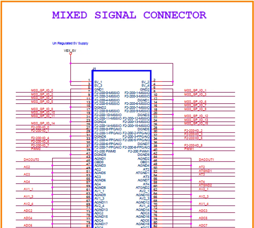
Break Out Board – Signal Connector
The second connector can be used to probe signals or build add on connectors. It does not connect to any other hardware specific to Microsemi.
Test Points – Signal
Test Points – Power
Test Points – Ground
Manufacturing Test Flow
The manufacturing test flow is explained in the following steps:
- Plug the J1 Header of the 50-100-CONV-SA Header into the J21 Header of A2F-DEV-KIT.
- Ensure a good contact is made and the connector goes all the way in.
- Plug-in the 5V supply on J1 of the A2F-DEV-KIT.
- Turn the switch SW6 in the ON position.
- Ensure that the LED5 lights up. This ensures that no shorts exist on the 50-100-CONV-SA board.
Note: If there is a failure in Step 2 or Step 5, please keep these boards aside and inform Microsemi.
Product Support
Microsemi backs its products with various support services including Customer Service, a Customer Technical Support Center, a web site, an FTP site, electronic mail, and worldwide sales offices. This appendix contains information about contacting Microsemi SoC Products Group (formerly Actel) and using these support services.
Customer Service
Contact Customer Service for non-technical product support, such as product pricing, product upgrades, update information, order status, and authorization.
- From Northeast and North Central U.S.A., call 650.318.4480
- From Southeast and Southwest U.S.A., call 650. 318.4480
- From South Central U.S.A., call 650.318.4434
- From Northwest U.S.A., call 650.318.4434
- From Canada, call 650.318.4480
- From Europe, call 650.318.4252 or +44 (0) 1276 401 500
- From Japan, call 650.318.4743
- From the rest of the world, call 650.318.4743
- Fax, from anywhere in the world 650.318.8044
Customer Technical Support Center
Microsemi staffs its Customer Technical Support Center with highly skilled engineers who can help answer your hardware, software, and design questions. The Customer Technical Support Center spends a great deal of time creating application notes and answers to FAQs. So, before you contact us, please visit our online resources. It is very likely we have already answered your questions.
Technical Support
Visit the Customer Support website (www.actel.com/support/search/default.aspx) for more information and support. Many answers available on the searchable web resource include diagrams, illustrations, and links to other resources on the website.
Website
You can browse a variety of technical and non-technical information on the SoC home page, at www.actel.com.
Contacting the Customer Technical Support Center
Highly skilled engineers staff the Technical Support Center from 7:00 a.m. to 6:00 p.m., Pacific Time, Monday through Friday. Several ways of contacting the Center follow:
Email
You can communicate your technical questions to our email address and receive answers back by email, fax, or phone. Also, if you have design problems, you can email your design files to receive assistance. We constantly monitor the email account throughout the day. When sending your request to us, please be sure to include your full name, company name, and your contact information for efficient processing of your request.
The technical support email address is [email protected].
Phone
Our Technical Support Center answers all calls. The center retrieves information, such as your name, company name, phone number and your question, and then issues a case number. The Center then forwards the information to a queue where the first available application engineer receives the data and returns your call. The phone hours are from 7:00 a.m. to 6:00 p.m., Pacific Time, Monday through Friday.
The Technical Support numbers are:
650.318.4460
800.262.1060
Customers needing assistance outside the US time zones can either contact technical support via email (s[email protected]) or contact a local sales office. Sales office listings can be found on the website at www.actel.com/company/contact/default.aspx.
Microsemi Corporation (NASDAQ: MSCC) offers the industry’s most comprehensive portfolio of semiconductor technology. Committed to solving the most critical system challenges, Microsemi’s products include high-performance, high-reliability analog and RF devices, mixed signal integrated circuits, FPGAs and customizable SoCs, and complete subsystems. Microsemi serves leading system manufacturers around the world in the defense, security, aerospace, enterprise, commercial, and industrial markets. Learn more at www.microsemi.com.
© 2011 Microsemi Corporation. All rights reserved. Microsemi and the Microsemi logo are trademarks of Microsemi Corporation. All other trademarks and service marks are the property of their respective owners.
Microsemi Corporate Headquarters
2381 Morse Avenue, Irvine, CA 92614
Phone: 949-221-7100
Fax: 949-756-0308
www.microsemi.com


