![]() UG0932 Image Scaler
UG0932 Image Scaler
User Guide
UG0932 Image Scaler
Microsemi makes no warranty, representation, or guarantee regarding the information contained herein or the suitability of its products and services for any particular purpose, nor does Microsemi assume any liability whatsoever arising out of the application or use of any product or circuit. The products sold hereunder and any other products sold by Microsemi have been subject to limited testing and should not be used in conjunction with mission-critical equipment or applications. Any performance specifications are believed to be reliable but are not verified, and Buyer must conduct and complete all performance and other testing of the products, alone and together with, or installed in, any end-products. Buyer shall not rely on any data and performance specifications or parameters provided by Microsemi. It is the Buyer’s responsibility to independently determine suitability of any products and to test and verify the same. The information provided by Microsemi hereunder is provided “as is, where is” and with all faults, and the entire risk associated with such information is entirely with the Buyer. Microsemi does not grant, explicitly or implicitly, to any party any patent rights, licenses, or any other IP rights, whether with regard to such information itself or anything described by such information. Information provided in this document is proprietary to Microsemi, and Microsemi reserves the right to make any changes to the information in this document or to any products and services at any time without notice.
About Microsemi
Microsemi, a wholly owned subsidiary of Microchip Technology Inc. (Nasdaq: MCHP), offers a comprehensive portfolio of semiconductor and system solutions for aerospace & defense, communications, data center and industrial markets.
Products include high-performance and radiation-hardened analog mixed-signal integrated circuits, FPGAs, SoCs and ASICs; power management products; timing and synchronization devices and precise time solutions, setting the world’s standard for time; voice processing devices; RF solutions; discrete components; enterprise storage and communication solutions, security technologies and scalable anti-tamper products; Ethernet solutions; Power-over-Ethernet ICs and midspans; as well as custom design capabilities and services. Learn more at www.microsemi.com.
Revision History
The revision history describes the changes that were implemented in the document. The changes are listed by revision, starting with the most current publication.
Revision 1.0
The first publication of this document.
Introduction
The Image Scaler provides both down-scaling and up-scaling ability to resize an image. The implementation uses a bilinear interpolation algorithm to resize the image. The input and output resolutions must be specified using the input ports that define the corresponding resolution.
The Image Scaler will operate in up-scaling mode when either the horizontal or vertical output image resolution is greater than or equal to the respective horizontal or vertical input image resolution.
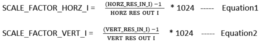
The horizontal and vertical scale factors should be provided as inputs to the IP that are calculated based on the horizontal and vertical resolution inputs to the IP using the equations below:
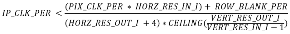
The image scaler accepts the input image pixel data in RGB 8-bit format at the pixel clock rate. When the scaler IP is operating in downscaler only mode, the IP clock (IP_CLK_I) can be connected to the SYS_CLK_I. When the scaler IP is operating in upscaler mode, the IP clock frequency should be higher than the pixel clock (SYS_CLK_I) frequency as per equation below:
SCALE_FACTOR_HORZ_I represents the image scaling in the horizontal resolution.
SCALE_FACTOR_VERT_I represents the image scaling in the vertical resolution.
HORZ_RES_IN_I represents the horizontal resolution of the input image.
HORZ_RES_OUT_I represents the horizontal resolution of the output image.
VERT_RES_IN_I represents the vertical resolution of the input image.
VERT_RES_OUT_I represents the vertical resolution of the output image.
IP_CLK_PER represents the clock period for the IP clock (IP_CLK_I).
PIX_CLK_PER represents the pixel clock period for the input image.
ROW_BLANK_PER represents the row blanking period for the input image.
The IP scaling ratio can be changed dynamically by changing the resolution inputs and the scale factors.
It is recommended to modify the scaling ratio only during frame blanking period. When the IP is dynamically switched between down scaling and upscaling, the IP clock should be calculated based on the maximum intended upscaling ratio.
Interface
This section describes the inputs and outputs and configuration parameters of the Image Scaler IP.
Inputs and Outputs
Image Scaler IP Block Diagram
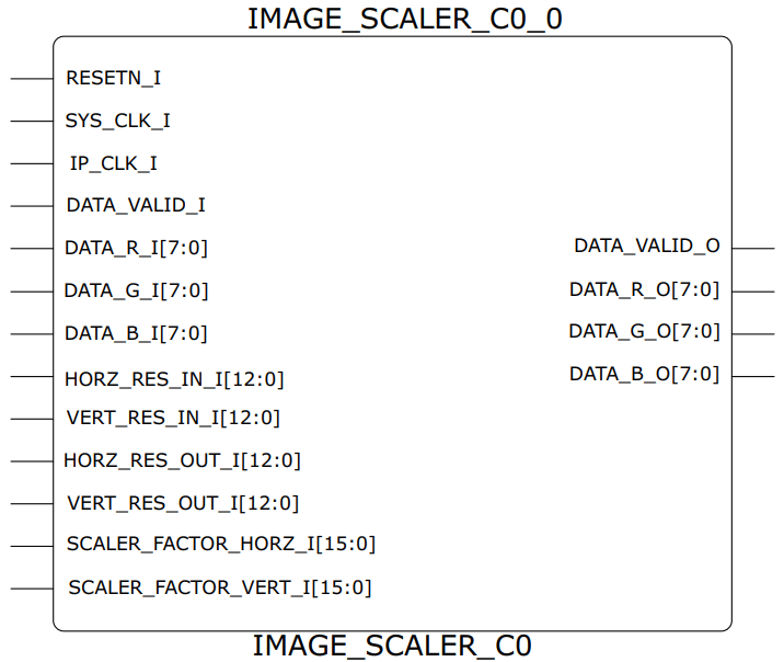
The following table lists the input and output ports of the Image Scaler IP.
Table 1 Input and Output Ports
| Port Name | Direction | Width | Description |
| SYS_CLK_I | Input | 1 bit | System clock. This must be the same as the pixel clock used in Equation3. |
| IP_CLK_I | Input | 1 bit | Scaler IP clock. Can reuse the SYS_CLK_I if the IP is only used for down-scaling. A separate clock that satisfies Equation3 is needed for up-scaling configuration. |
| RESETN_I | Input | 1 bit | Active low asynchronous reset signal to design. |
| DATA_VALID_I | Input | 1 bit | Input data valid signal. This signal should be asserted when the data is valid. |
| DATA_R_I | Input | 8 bits | Input Red pixel data. DATA_R_I [G_DATA_WIDTH -1] |
| DATA_G_I | Input | 8 bits | Input Green pixel data. DATA_G_I [G_DATA_WIDTH -1] |
| DATA_B_I | Input | 8 bits | Input Blue pixel data. DATA_B_I [G_DATA_WIDTH -1] |
| HORZ_RES_IN_I | Input | 13 bits | Horizontal resolution of the input image in pixels. HORZ_RES_IN_I [12:0] |
| VERT_RES_IN_I | Input | 13 bits | Vertical resolution of the input image in lines. VERT_RES_IN_I [12:0] |
| HORZ_RES_OUT_I | Input | 13 bits | Horizontal resolution of the output image in pixels. HORZ_RES_OUT_I [12:0] |
| VERT_RES_OUT_I | Input | 13 bits | Vertical resolution of the output image in lines. VERT_RES_OUT_I [12:0] |
| SCALE_FACTOR_HORZ_I | Input | 16 bits | Scaling factor for width. It can be calculated as shown in Equation1. |
| SCALE_FACTOR_VERT_I | Input | 16 bits | Scaling factor for height. It can be calculated as shown in Equation2. |
| DATA_VALID_O | Output | 1 bit | Output data valid signal. This signal is asserted when the output data is valid. |
| DATA_R_O | Output | 32 bits | Output Red pixel data DATA_R_O [G_DATA_WIDTH -1] |
| DATA_G_O | Output | 8 bits | Output Green pixel data DATA_G_O [G_DATA_WIDTH -1] |
| DATA_B_O | Output | 8 bits | Output Green pixel data DATA_G_O [G_DATA_WIDTH -1] |
3.2 Configuration Parameters
The following table lists the configuration parameters used in the hardware implementation of the Image Scaler. These parameters are generic and can be varied based on the application requirement.
Table 2 • Configuration Parameters
| Parameter Name | Description |
| G_DATA_WIDTH | Represents bit width of the input and output data. The current version is only tested to support 8-bit input and output data. |
| G_INPUT_FIFO_AWIDTH | Represents Depth of the input FIFO used to store one row of the input image. 2^(G_INPUT_FIFO_AWIDTH) must be sufficient to store one entire row of the input image. |
| G_OUTPUT_FIFO_AWIDTH | Represents depth of the output FIFO used to store one row of the output image. 2^(G_OUTPUT_FIFO_AWIDTH) must be sufficient to store one entire row of the output image. |
Testbench
A Testbench is provided to check the functionality of the Image Scaler IP. To ensure that the Testbench works correctly, the configuration parameters listed in Table 3 must be configured at the beginning of the Testbench file.
Table 3 • Testbench Configuration Parameters
| Name | Description |
| HORZ_RES_IN | Horizontal resolution of the input image |
| VERT_RES_IN | Vertical resolution of the input image |
| HORZ_RES_OUT | Horizontal resolution of the scaled output image |
| VERT_RES_OUT | Vertical resolution of the scaled output image |
| SCALE_FACTOR_HORZ_I | Scale factor in horizontal direction – Formula and example provided as comment. |
| SCALE_FACTOR_VERT_I | Scale factor in vertical direction – Formula and example provided as comment. |
| SYSCLKPERIOD | Pixel clock period of the input image |
| IPCLKPERIOD | Desired frequency for the Scaler IP It can reuse SYSCLKPERIOD for down-scaling It must satisfy Equation 3 for up-scaling |
| BLANK_PER | Blanking period between consecutive rows for input image |
| INPUT_IMG_FILE_NAME | Location and name of the input image file |
| OUTPUT_IMG_FILE_NAME | Location and name of the generated scaled image file |
Before running simulation, ensure that the image scaler instance was generated with sufficient input and output FIFO depth. Ensure that G_INPUT_FIFO_AWIDTH, G_OUTPUT_FIFO_AWIDTH values provided in the configurator GUI are correct.
The following steps describe how to simulate the core using the Testbench. The packaged Testbench will upscale an input image with a 960×540 resolution to produce an output image with a 1280×720 resolution.
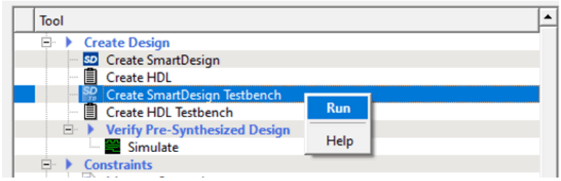
1. In the Design Flow window, expand Create Design, right-click Create Smartening Testbench, and click Run, as shown in the following figure.
Figure 2 • Create Smartening Testbench
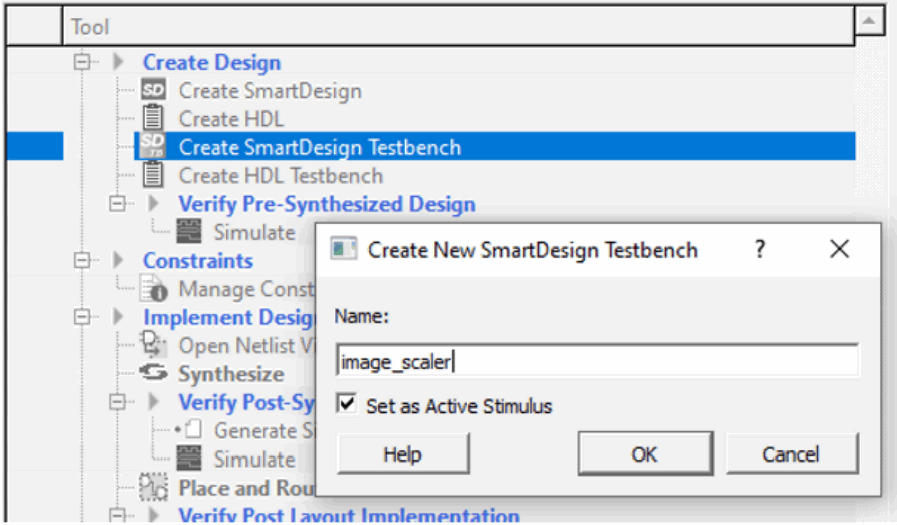
2. Enter name for the Smartening Testbench, and click OK.
Figure 3 • Smartening Testbench Name
SmartDesign testbench is created, and a canvas appears to the right of the Design Flow pane.
3. In the Libero SoC Catalog (View > Windows > Catalog), expand Solutions-Video, and drag the
Scaler IP core onto the Smart Design Testbench canvas.
Figure 4 • Scaler IP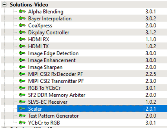
4. Select the default component name and click OK.
Figure 5 Create Component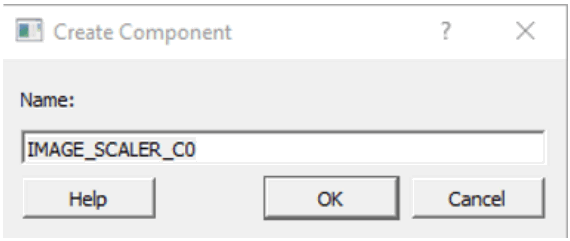
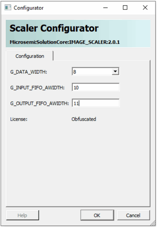
5. In the Scaler Configurator GUI window, update the G_INPUT_FIFO_AWIDTH to 10, G_OUTPUT_FIFO_AWIDTH to 11, then click OK.
Figure 6 Scaler Configurator
6. Select all the ports on the IMAGE_SCALER_C0 instance, right-click, and select Promote to Top Level, as shown in the following figure.
Figure 7 Image Scaler Ports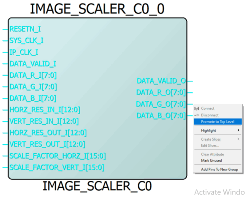
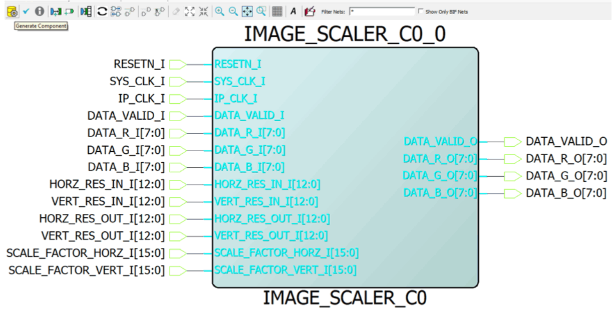
7. Click Generate Component from the Smart Design toolbar, as shown in the following figure.
Figure 8 • Generate Component
8. Go to the Files tab and select simulation > Import Files…, as shown in the following figure.
Figure 9 Import files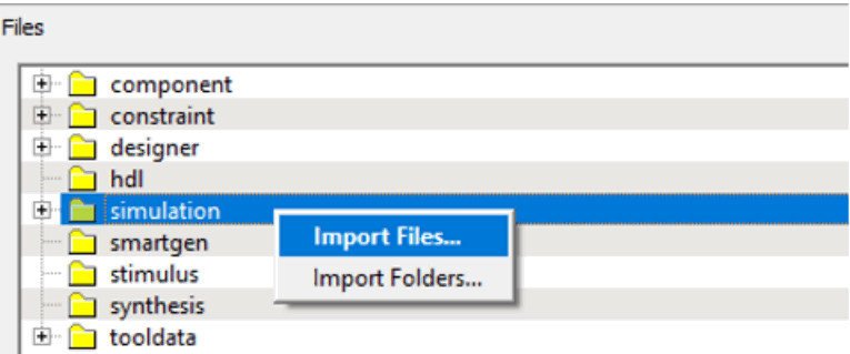
Import the Input Image file “Input_Image_960_540.txt” from the following path:
\<Project name>\component\Microsemi\Solution Core\IMAGE_SCALER\2.0.1\Stim lush. To import a different file, browse the folder that contains the required file, and click Open. The imported file is listed under simulation, as shown in the following figure.
Figure 10 • Input Image file
10. On the Design Hierarchy tab, click Build Hierarchy, then right-click IMAGE_SCALER_C0 and click Set As Root.
Figure 11 Design Hierarchy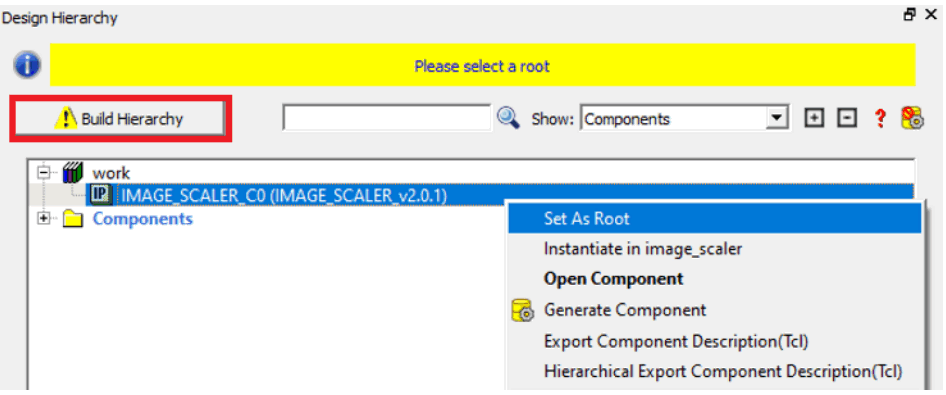
11. On the Stimulus Hierarchy tab, right-click image_scaler_test Testbench file and click Open Interactively from Simulate Pre-Synth Design.
Figure 12 • Stimulus Hierarchy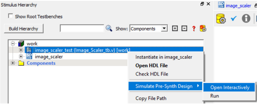
The Modelist tool appears with the Testbench file loaded on to it, as shown in the following figure.
Figure 13 Modelist tool
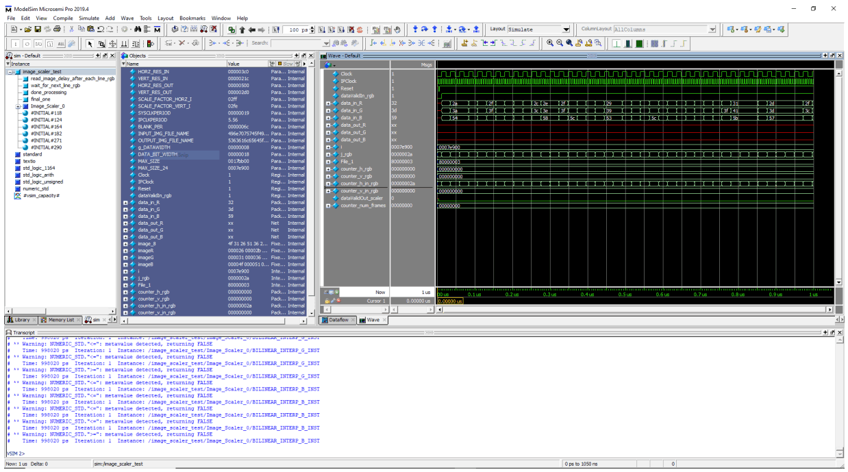
If the simulation is interrupted because of the runtime limit in the DO file, use the run -all command to complete the simulation. By default, the output image file is placed in the Files/simulation directory and uses the OUTPUT_IMG_FILE_NAME.
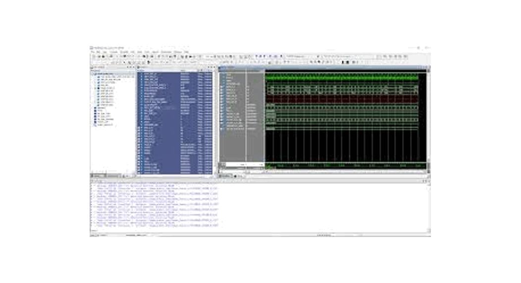
Simulation Results
5.1 Timing Diagram
The following is the timing diagram for Scaler IP showing video data and control signals for the first two rows of the output image.
Figure 14 • Video data and Control signals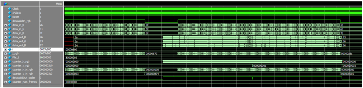
Table 4 • Timing Diagram Configuration Parameters
| Name | Description |
| datalink_(R, G, B) | Input image pixel data |
| data out_(R, G, B) | Scaled output image pixel data |
| counter_h_rgb | Counter tracking the number of scaled output image rows |
| counter_h_rgb | Counter tracking the number of scaled output image pixels per row |
| dataValidOut_scaler | Data valid signal generated by Scaler IP |
| counter_num_frames | Number of input image frames processed |
5.2 Output Image
As mentioned earlier, the packaged Testbench will upscale an input image with a 960×540 resolution to produce an output image with a 1280×720 resolution. The scaled output image is shown in the following figure.
Figure 15 • Scaled output
Resource Utilization
Image Scaling is implemented on PolarFire FPGA (MPF100T -1FCG484 package). The following table shows the resource utilization report after synthesis.
Table 5 • Resource Utilization
| Resource | Usage |
| DFFs | 1487 |
| 4LUTs | 1811 |
| RAM1K20 | 11 |
| MACC | 13 |
Note: G_DATA_WIDTH = 8, G_INPUT_FIFO_AWIDTH = 11, and G_OUTPUT_FIFO_AWIDTH = 10.
Microsemi Proprietary and Confidential UG0932 User Guide Revision 1.0
![]() Microsemi Headquarters
Microsemi Headquarters
One Enterprise, Aliso Viejo,
CA 92656 USA
Within the USA: +1 (800) 713-4113
Outside the USA: +1 (949) 380-6100
Sales: +1 (949) 380-6136
Fax: +1 (949) 215-4996
Email: [email protected]
www.microsemi.com
©2020 Microsemi, a wholly owned
subsidiary of Microchip Technology Inc. All rights reserved. Microsemi and the
Microsemi logo are registered trademarks of
Microsemi Corporation. All other trademarks and service marks are the property of their respective owners.


