![]() UG0651 Smart Fusion 2 FPGAs
UG0651 Smart Fusion 2 FPGAs
User Guide
UG0651 Scaler
Revision History
The revision history describes the changes that were implemented in the document. The changes are listed by revision, starting with the most current publication.
1.1 Revision 5.0
In revision 5.0 of this document, the Resource Utilization section and the Resource Utilization Report were updated. For more information, see Resource Utilization (see page 15).
1.2 Revision 4.0
In revision 4.0 of this document, the Steps to simulate the core using test bench was added. For more information, see Test Bench (see page 8) .
1.3 Revision 3.0
The following is a summary of changes in revision 3.0 of this document.
- Updated the Configuration Parameters table. For more information, see Test bench Configuration. Parameters (see page 8)
- Updated the timing diagram. For more information, see Timing Diagram (see page 7) .
- Added the Information about image buffer 0 and image buffer 1. For more information, see. Hardware Implementation (see page 4)
- Updated the Information about FSM states. For more information, see FSM Implementation (see. page 6)
1.4 Revision 2.0
The following is a summary of changes in revision 2.0 of this document.
Added the Test bench Configuration Parameters table. For more information, see Test bench. Configuration Parameters (see page 8)
Updated the tables such as, Scaler Input and Output Ports and Resource Utilization Report. For more information, see Inputs and Outputs (see page 5) and Resource Utilization Report (see page 15) .
Updated the figures such as, Scaler Block Diagram and Timing Diagram. For more information, see and Scalar Block Diagram (see page 4) Timing Diagram (see page 7).
1.5 Revision 1.0
Revision 1.0 is the first publication of this document.
Introduction
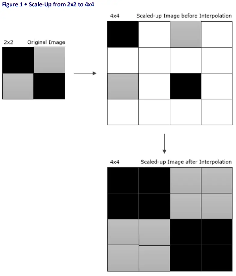
Image scaling is a process of constructing a resized image from a given input image. The constructed image can be smaller, larger, or equal in size, depending on the scaling ratio. While scaling up an image, empty spaces are introduced in the base image. The following figure shows an image at its original dimensions (2×2) and at scaled-up dimensions (4×4). The white pixels represent empty spaces where interpolation is required, and the complete picture is the result of the nearest neighbor interpolation.
Interpolation algorithms attempt to generate continuous data from a set of discrete data samples through an interpolation function. The interpolation algorithms minimize the visual defects arising from the inevitable resampling error and improve the quality of the resampled images. The interpolation function is performed by the convolution operation that involves a large number of additions and multiplications. However, a trade-off is required between the computation complexity and quality of the scaled image. Based on the content awareness of the algorithm, the image scaling algorithms are classified as adaptive image scaling and non-adaptive image scaling.
Adaptive image scaling algorithms modify their interpolation technique based on whether the image has a smooth texture or a sharp edge. The interpolation method changes in real-time, therefore these algorithms are complex and computationally intensive. They find widespread use in image editing software, as they ensure a high quality scaled image.
Non-adaptive image scaling algorithms such as nearest neighbor, bilinear, bicubic, and Lenclos algorithms have a fixed interpolation method irrespective of the image content.
Using the nearest neighbor algorithm, image scaling is performed by interpolating a pixel’s color and intensity values (horizontally and vertically) based on the values of neighboring pixels. The nearest neighbor algorithm is used to find the empty spaces in the original image, and to replace them with the nearest neighboring pixel.
Hardware Implementation
The scaler module contains two internal buffers that can store one line of the image for processing—Image_Buffer0_i and Image_Buffer1_i. Each line of input data is written to Image_Buffer0_i and Image_Buffer1_i, alternately. The line_ready signal indicates that the scaler can start processing the next line. It must be set to high after the input line write to the buffer is completed.
With the exception of the first line, after one line of data is input to the scaler, the next line must be input only after the Line_Done_o signal goes high. For a new frame, the first two lines of the frame need to be input before the scaler starts processing the data.
The data stored in the image buffer is scaled to calculate the output data based on the nearest neighbor algorithm.
When downscaling the height of the image, the next input line to the scaler must begin with the pixel number mentioned in NxtLine_PixelNum_Offset_o. When upscaling, the value of NxtLine_PixelNum_Offset_o is the first pixel of the next line in sequence.
The following equations are used to calculate scaling factors for horizontal and vertical resolutions.
X= x /x x 2g scaling_bitwidth scale_factor
Y= y /y x 2 g scaling_bitwidth scale_factor
The following figure shows the scaler block diagram.
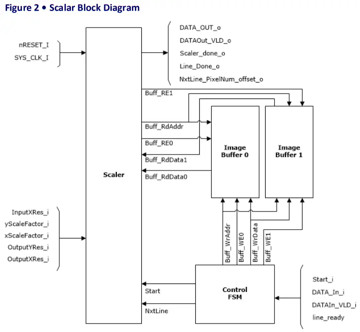
3.1 Inputs and Outputs
The following table describes the input and output ports.
Table 1 • Inputs and Outputs
| Signal Name | Direction | Width | Description |
| nReset_I | Input | – | Active low asynchronous reset |
| signal to design. | |||
| SYS_CLK_I | Input | – | System clock. |
| DATA_In_i | Input | [g_DATA_BITWIDTH * g_CHANNELS – 1: 0] | Input data to scaler. |
| DATAIn_VLD_i | Input | – | Set when input data is valid. |
| Start_i | Input | – | Scaler start signal. To be set to high before loading a new frame. |
| InputXRes_i | Input | [g_INPUT_X_RES_BITWIDTH – 1 : 0] | Input image width resolution. |
| OutputXRes_i | Input | [g_OUTPUT_X_RES_BITWIDTH – 1 : 0] | Output image width resolution. |
| OutputYRes_i | Input | [g_OUTPUT_Y_RES_BITWIDTH – 1 : 0] | Output image height resolution. |
| xScaleFactor_i | Input | [g_SCALE_FACTOR_BITWIDTH – 1 : 0] | Width scale factor. |
| yScaleFactor_i | Input | [g_SCALE_FACTOR_BITWIDTH – 1 : 0] | Height scale factor. |
| Scaler_done_o | Output | – | Set to high for one clock cycle of system clock when the scaler completes scaling of one frame. |
| Line_Done_o | Output | – | Set to high after one line is processed. |
| NxtLine_PixelNum_Offset_o | Output | [(g_INPUT_Y_RES_BITWIDTH+g_INPUT_ X_RES_BITWIDTH – 1): 0] | Indicates the pixel number of the source image from which the next line is to be dumped into the scaler image buffer. |
| DATA_OUT_o | Output | [g_DATA_BITWIDTH * g_CHANNELS – 1 : 0] | Scaled data output. |
| DATAOut_VLD_o | Output | – | Sets when output data is a valid register and describes the output of the scaler. |
| line_ready | Input | – | Set when writing the current line to the image buffer is complete, indicating that buffer data is ready for processing. |
3.2 Configuration Parameters
The following table describes the configuration parameters used in the hardware implementation of the scaler. These are generic parameters and can vary based on the application requirements.
Table 2 • Configuration Parameters
| Signal Name | Description |
| g_DATA_BITWIDTH | Width of the data input or output |
| g_CHANNELS | Number of data channels |
| g_INPUT_X_RES_BITWIDTH | Input resolution X bit width |
| g_INPUT_Y_RES_BITWIDTH | Input resolution Y bit width |
| g_OUTPUT_X_RES_BITWIDTH | Output resolution X bit width |
| g_OUTPUT_Y_RES_BITWIDTH | Output resolution Y bit width |
| g_SCALE_FACTOR_BITWIDTH | Scaling factor bit width |
| g_SF_ROUNDING_PRECISION | Scaling factor’s rounding precision bit width. Default value is configured to 256 (28). |
| g_BUFF_DEPTH | Line buffer depth |
3.3 FSM Implementation
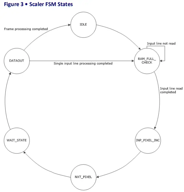
The scaler finite state machine (FSM) goes through the following states during implementation.
- IDLE: After the module is reset or frame processing is complete, the FSM goes to IDLE state and waits for the start signal to move to the RAM_FULL_CHECK state.
- RAM_FULL_CHECK: The FSM remains in this state until the write to the image buffer is completed and line_ready signal is received. Then, it moves to the
- INP_PIXEL_INC state.
- INP_PIXEL_INC: The FSM moves to the NXT_PIXEL state in the next cycle.
- NXT_PIXEL: The FSM moves to WAIT_STATE in the next cycle.
- WAIT_STATE: The FSM moves to DATAOUT state in the next cycle.
- DATAOUT: The output pixel is calculated based on the horizontal counter, vertical counter, and scaling factors. The horizontal and vertical counters are updated and the read address and read enable signal (for reading from one of the two image buffers) is generated. On completion of processing of one input line, the FSM moves to RAM_FULL_CHECK state. After the total frame data is output, the FSM moves to IDLE state.
The following figure shows the scaler FSM implementation.
3.4 Timing Diagrams
The following figure shows the timing diagram of the scaler.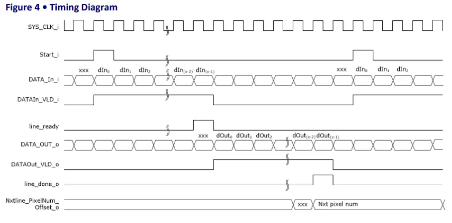
3.5 Test bench
A test bench is provided to check the functionality of the scaler core. The following table lists the parameters that can be configured according to the application.
Table 3 • Test bench Configuration Parameters
| Name | Description |
| CLKPERIOD | Clock Period |
| IN_HEIGHT | Height of the input image |
| IN_WIDTH | Width of the input image |
| OUT_HEIGHT | Height of the output frame |
| OUT_WIDTH | Width of the output frame |
| IMAGE_FILE_NAME | Input file name |
The following steps describe how to simulate the core using the test bench.
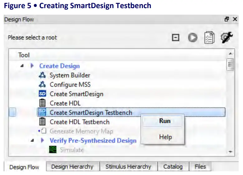
- In the Design Flow window, expand Create Design . Right-click Create Smart Design Test bench and click Run as shown in the following figure.

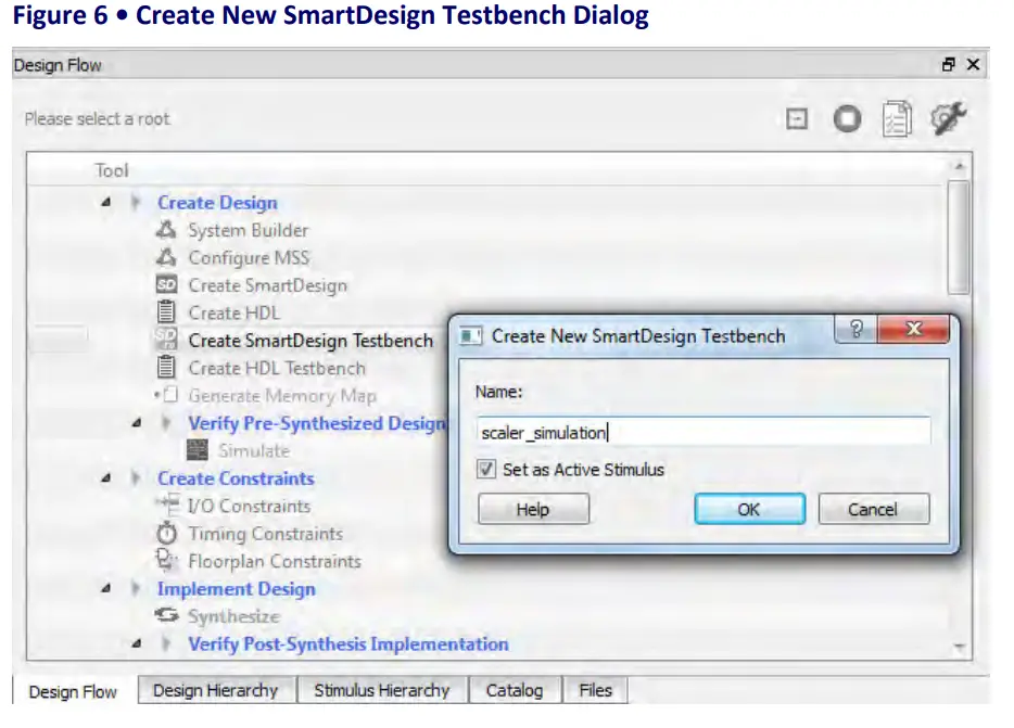
- In the Create New Smart Design Test bench dialog box, enter a name and click OK .
 Smart Design test bench is created, and a canvas appears to the right of the Design Flow pane.
 - In the Libero SoC Catalog window, expand Solutions-Video , and drag the Scaler core onto the Smart Design test bench canvas.
 The core appears on the canvases shown in the following figure.
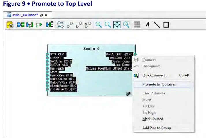
- Select all the ports of the core, right-click and select Promote to Top Level as shown in the following figure.
 The ports are promoted to the top level as shown in the following figure.
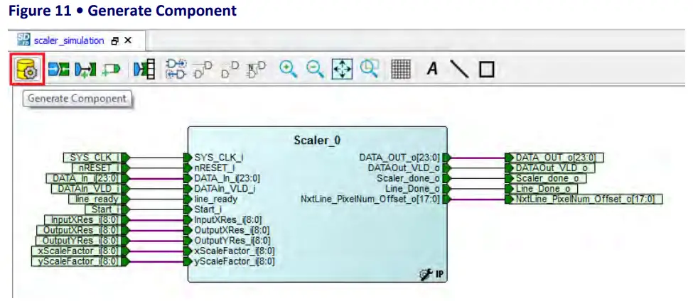
- On the Smart Design toolbar, click Generate Component highlighted in the following figure. The Smart Design component is generated.

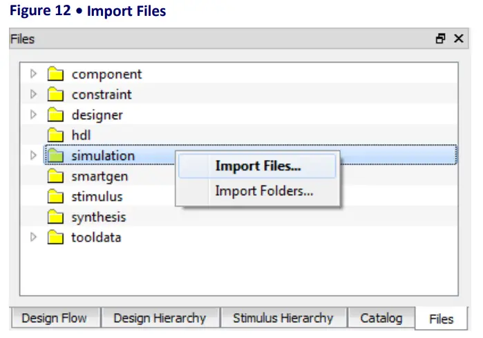
- In the Files window, right-click simulation and click Import Files… as shown in the following figure.

- Do one of the following:
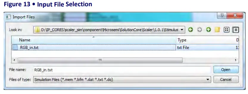
• To import the sample test bench input file, browse to sample test bench input file to the stimulus directory and click Open as shown in the following figure. A sample RGB_in.txt file is provided with the test bench at the following path: ..\Project_name\component\Microsemi\SolutionCore\Scaler\2.0.0 \Stimulus
• To import a different file, browse to the folder containing the image file and click Open . The imported file is listed under simulation as shown in the following figure.
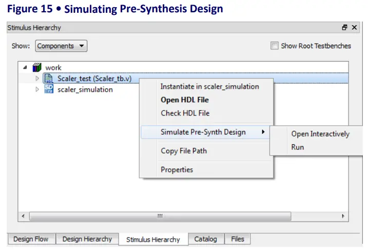
- From Stimulus Hierarchy window expand Work , right-click ( ) and select Scaler_test Scaler_tb.v Simulate Pre-Synth Design and then click Open Interactively. The core is simulated for one frame.
 The Modalism tool appears with the test bench file loaded into its shown in the following figure.
 If the simulation is interrupted because of the runtime limit specified in the file, use the DO run – command to complete the simulation. After the simulation is completed, the test bench output all image file appears in the simulation folder.
 Smart Design test bench is created, and a canvas appears to the right of the Design Flow pane.
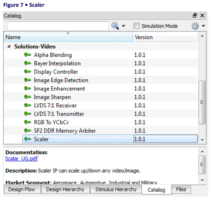 The core appears on the canvases shown in the following figure.
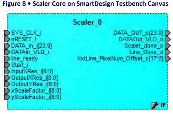
 The ports are promoted to the top level as shown in the following figure.
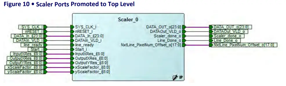
 The imported file is listed under simulation as shown in the following figure.
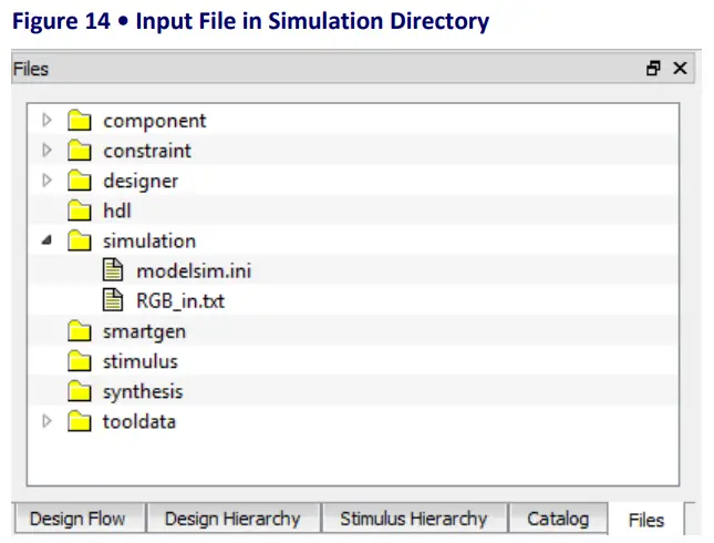
 The Modalism tool appears with the test bench file loaded into its shown in the following figure.
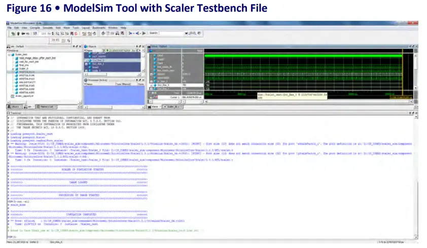 If the simulation is interrupted because of the runtime limit specified in the file, use the DO run – command to complete the simulation. After the simulation is completed, the test bench output all image file appears in the simulation folder.
3.6 Resource Utilization
The scaler is implemented in the SmartFusion®2 system-on-chip (SoC) FPGA (M2S150T-1FC1152 package) and Polar Fire FPGA (MPF300TS_ES-1FCG1152E package). The following table lists the resources used by the FPGA.
Table 4 • Resource Utilization Report
| Resource | Usage |
| DFFs | 328 |
| 4-Input LUTs | 510 |
| MACC | 3 |
| RAM1Kx18 | 2 |
| RAM64x18 | 0 |
Microsemi makes no warranty, representation, or guarantee regarding the information contained herein or the suitability of its products and services for any particular purpose, nor does Microsemi assume any liability whatsoever arising out of the application or use of any product or circuit. The products sold hereunder and any other products sold by Microsemi have been subject to limited testing and should not be used in conjunction with mission-critical equipment or applications. Any performance specifications are believed to be reliable but are not verified, and Buyer must conduct and complete all performance and other testing of the products, alone and together with, or installed in, any end-products. Buyer shall not rely on any data and performance specifications or parameters provided by Microsemi. It is the Buyer’s responsibility to independently determine suitability of any products and to test and verify the same. The information provided by Microsemi hereunder is provided “as is, where is” and with all faults, and the entire risk associated with such information is entirely with the Buyer. Microsemi does not grant, explicitly or implicitly, to any party any patent rights, licenses, or any other IP rights, whether with regard to such information itself or anything described by such information. Information provided in this document is proprietary to Microsemi, and Microsemi reserves the right to make any changes to the information in this document or to any products and services at any time without notice.
Microsemi Corporation (Nasdaq: MSCC) offers a comprehensive portfolio of semiconductor and system solutions for aerospace & defense, communications, data center and industrial markets. Products include high-performance and radiation-hardened analog mixed-signal integrated circuits, FPGAs, SoCs and ASICs; power management products; timing and synchronization devices and precise time solutions, setting the world’s standard for time; voice processing devices; RF solutions; discrete components; enterprise storage and communication solutions; security technologies and scalable anti-tamper products; Ethernet solutions; Power-over-Ethernet ICs and midspans; as well as custom design capabilities and services.
Microsemi is headquartered in Aliso Viejo, California, and has approximately 4,800 employees globally. Learn more at www.microsemi.com.![]()
Microsemi Corporate Headquarters
One Enterprise, Aliso Viejo,
CA 92656 USA
Within the USA: +1 (800) 713-4113
Outside the USA: +1 (949) 380-6100
Fax: +1 (949) 215-4996
Email: [email protected]
www.microsemi.com
© 2018 Microsemi Corporation. All rights reserved. Microsemi and the
Microsemi logo are trademarks of Microsemi Corporation. All other
trademarks and service marks are the property of their respective owners.
UG0651 User Guide Revision 5.0
50200651


