ABB SEMIS Simulation Tool Isolated DC-DC Converter
INTRODUCTION
SEMIS is a web-based semiconductor simulation tool providing a thermal calculation of the semiconductor losses for common converter circuits. The simulation simplifies significantly the selection of the switching de-vice and enables the optimal selection of semiconductors for further investigations.
The SEMIS Simulation Tool is a user-friendly online application found on ABB Semiconductors website www.abb.com/semi-conductors/semis
SEMIS users select from a substantial selection of topologies. By assigning the circuit parameters and selecting the desired switching device, multiple ABB products can be simulated at the same time. Once a simulation is run, SEMIS returns comprehensive results on semiconductor losses as well as on the electrical parameters in the input and output of the circuit. The results are shown in both graphical (waveforms) and numerical (tables) way. The SEMIS tool is based on the PLECS simulation software. PLECS users can download our product models in the XML file format from the ABB Semiconductors website and use them for their simulations. For more specific topologies ABB offers customized converter simulations for non-standard topologies with PLECS simulation software on a project basis.
COPYRIGHTS
All rights to copyrights, registered trademarks, and trademarks reside with their respective owners.
Copyright © 2020 ABB Power Grids Switzerland Ltd.
All rights reserved.
Release: April 2020
Document number: 5SYA 2134
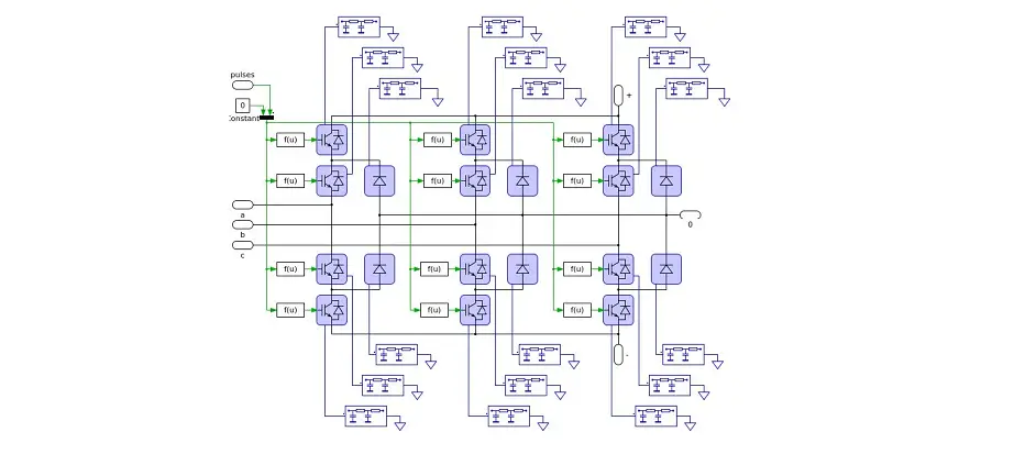
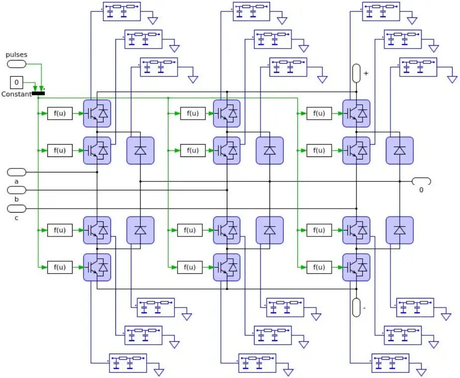
ISOLATED DC-DC CONVERTER MODELS
Isolated DC-DC converters are used to generate regulated DC output voltage with electrical isolation from the input supply. Linear supplies are commonly larger in size with 50-60Hz transformers in comparison to DC-DC converters with high frequency (HF) transformers. The overall efficiency of linear power supplies is usually of the range 30-60%, both these shortcomings are addressed by Isolated DC-DC converters.
ABB offers the following Isolated DC-DC converters for thermal analysis simulation in Isolated DC-DC converters 2:
- Isolated Push-pull converter
- Isolated Half-bridge converter
- Isolated full-bridge converter
Furthermore, ABB offers the following DC-DC converters for thermal analysis simulation:
- Non-Isolated Buck converter (Uout < Uin)
- Non-Isolated Boost converter (Uout > Uin)
- Non-Isolated Buck-Boost converter (Uout <> Uin)
- Isolated Fly back converter (Derived from Buck-Boost converter)
- Isolated Forward converter (Derived from step-down converter)
OVERVIEW
 Page layout of Non-Isolated DC-DC Converters in the ABB semiconductors website.
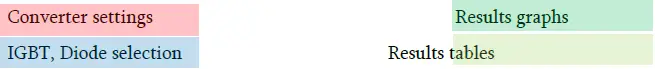
SIMULATION SETTINGS
Circuit parameters
Converter settings
The user can choose between the 3 types of converters here. All three of them can be used for step-up and step-down operations as the user can set the number of turns of the transformer. However, the user shall choose the input/output voltages, number of turns such that the duty ratio is less than 0.5. These converters are modeled to operate in Continuous Conduction Mode (CCM), one shall change the user inputs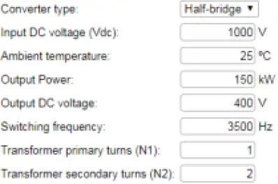 Converter settings input blocks
Coverter settings input blocks to operate the converters in CCM. An assertion has been set-up to let the user know when the converters fall into Discontinuous Conduction Mode (DCM).
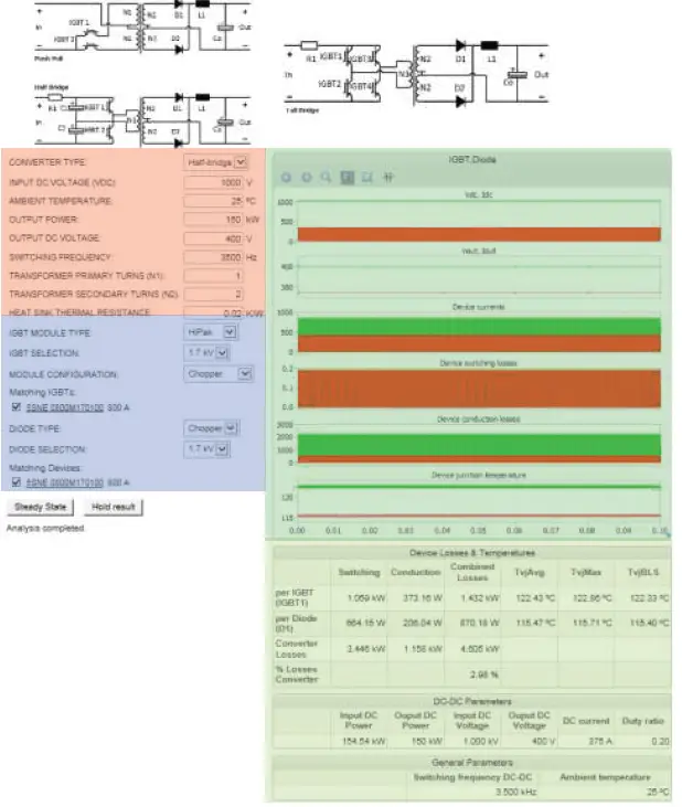
| CONVERTER TYPE | Converter is operated as Push-pull/Half-Bridge/FB | Selection |
| DC VOLTAGE INPUT | DC input voltage given by the user. Generally, this is the output of AC-DC converter | Range 10 .. 4500 V |
| AMBIENT TEMPERATURE | Definition of environmental temperature around the converter for temperature / cooling calculations | Range -25 .. 90 °C |
| OUTPUT POWER | Power demand of the load | Range 1 .. 150 kW |
| OUTPUT DC VOLTAGE§ | The constant DC output voltage on the load | Range 30 .. 1000V |
| SWITCHING FREQUENCY | Frequency at which the IGBT is turned ON/OFF | Range 200 .. 5000 Hz |
| TRANSFORMER PRIMARY TURNS (N1) | No of primary turns | Range 1 .. 30 |
| TRANSFORMER SECONDARY TURNS (N2) | No of secondary turns | Range 1 .. 30 |
Device settings
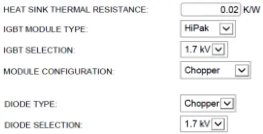 Thermal settings and device selection
HEAT SINK THERMAL RESISTANCE
Range 0.0001 .. 0.5 K/W
Definition of thermal resistance of the cooling system applied.
Remark: The value entered is attributed to each individual switch is shown in the electrical configuration schematic of the IGBT module datasheet. Therefore, if a user selects a dual switch module, the Rth should be multiplied with a factor of 2 to differentiate from the single switch case, if the same heatsink would be used in both cases.
The selected Rth is also accounted for the diode position for which the same consideration applies for its electrical configuration.
IGBT MODULE TYPE Select housing type of IGBT for filtering Selection
IGBT/DIODE SELECTION Select voltage class of IGBT for filtering Selection
MODULE CONFIGURATION Select topology of IGBT module for filtering Selection
Matching Devices
Once the previous IGBT and Diode properties are selected the matching IGBT and Diode options appear. By clicking on the product code name the user may access the datasheet from the ABB website.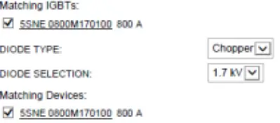 Matching IGBTs and Diodes for selection
Users can select the desired IGBTs and Diodes product names for simulation.
Up to 4 elements can be selected simultaneously and simulated. If one or more elements produce results exceeding the safe operating area (SOA) then they will return no results. In this case, the user should run the simulation again with changed parameters and/or product selection to enable results within SOA operating conditions.
Selection of articles / Start simulation
To simulate one or more articles, select from the list by activating the checkbox
Simulate
Starts the simulation The progress of the simulation is shown with the number of calculated Jacobians.
Abort
Stops the simulation; No results generated
Hold results
To compare multiple simulations, results can be held for later viewing By selecting the button, results are held after the simulation has finalized for later comparison with succeeding simulations![]() Start of simulation
Start of simulation ![]() Calculate Jacobian: 7/15
Calculate Jacobian: 7/15
Simulation progress and termination
SIMULATION RESULTS
The simulation results are displayed in two different ways for all selected articles simulated.
To hide curves of selected articles, unselect in the table “Results History”
Graphical results Visual analysis of waveforms for fast and efficient detection of most significant sources
Numerical results Numeric indication of all simulations values for direct comparison
Graphical Output – Waveforms
When the simulation finishes the semiconductor and DC side waveforms are appearing as follows: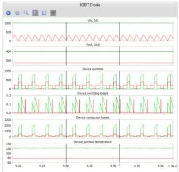 Graphical results of Half-bridge converter
Control
For an indication of values within the graph, a cursor can be activated to show curve values in a table. Sections of graphs can be zoomed in by click, move and release mouse button for more details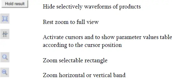 Parameters values indication
Tabular indication of graphical waveforms values according to cursor position selected. Values are indicated for each parameter Color of the waveform is indicated. The third column shows the difference between the two cursors per parameter.
Remark:
The numerical values of Phase Voltage/Current at the position of respective cursors are shown in the Table.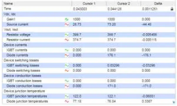 Tabular indication of cursor position graph values
Remark:
The numerical values of Voltage/Current at the position of respective cursors are shown in the Table. The numer-ical values of IGBT current/Diode Current along with their Switching loss, Conduction loss and Junction temperatures at the position of respective cursors are shown in the Table.
Numerical / Tabular results
The following parameters are given in a tabular format in multiple sections. All calculations and simulation results are based on datasheet typical values. All types of semiconductor losses are calculated according to the PLEXIM PLECS software principle through the reference of the lookup table and linear interpolation of the actual device current, voltage and junction temperature. As converter losses, the aggregated losses in all devices are accounted for. The losses per device are tabulated, the combined losses are calculated by multiplying the losses per device with the number of devices at the back-end as the all the IGBTs carry the same current and block the same voltage, same with the diodes.
Device Losses & Temperatures 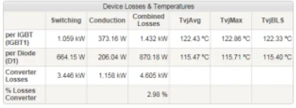 Device Losses & Temperatures
Switching Loss Single IGBT or Diode Losses during turn on and turn off events (dynamic)
Conduction loss Single IGBT or Diode Losses during on state (static)
Combined losses Sum of single IGBT or Diode switching and conduction loss.
Converter losses Sum of all IGBT and Diode losses
% Losses Defined as the (%) ratio of calculated combined converter losses with respect to the total output power and losses i.e., total apparent power flow.
Junction Temperature Avg
Junction temperature average during the simulation period
Junction Temperature Max
Maximum junction temperature during the simulation period
Junction Temperature BLS
Junction temperature at the time point just before the switching, after which the maximum junction temperature is achieved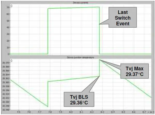 Definition of Tvj before the last switch
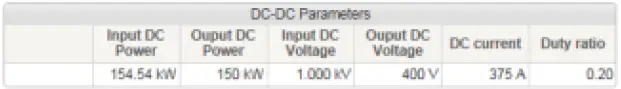 Converter DC-DC Parameters
DC-DC parameters
Input DC power
Active power supplied by the source including the thermal losses
Output DC power
Load power set by the user as explained in section 3.1.1
Input DC voltage
DC voltage supplied at the input of the converter (Usually the output of a rectifier)
Output DC voltage
DC voltage output set by the user as explained in section 3.1.1.
DC Current
DC current as drawn by the load at the power set by the user.
Duty ratio
Duty ratio is calculated and displayed as per section 6.
General parameters
 General Parameters
Switching Freq.
According to the definition
Ambient Temp.
According to the definition
ALERTS & FEATURES
The system verifies results and generated warning messages in case of limits are violated.
Parameter
Junction temperature
Verification
If the average junction temperature of IGBT and/or diode is above its maximum junction temperature limit, the alert message is displayed
Warning message
IGBT temperature out of the safe operating area
Parameter
DC Blocking voltage
Verification
If the voltage rating of the IGBT and/or diode is less than the DC blocking voltage, the alert message is displayed
Warning message
For the selected device voltage rating, the operating range of the device is dis-played
Parameter
Duty ratio
Verification
Range of Duty ratio is 0 .. 0.5. If the duty ratio is out of these limits the alert message is displayed
Warning message(s)
The maximum duty ratio cannot exceed 0.5 for the Half-Bridge DC-DC converter. Please check your input voltage, output voltage and turns ratio
APPLIED CALCULATIONS
Input Parameter Definitions
VDC
Input DC voltage
VOUT
Output DC voltage
N2
Transformer secondary turns
N1
Transformer primary turns
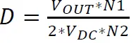
Duty ratio of the converter
The following calculations have been used in the model to calculate the duty ratio:
Push-Pull (PP), Full Bridge (FB)
Half Bridge (HB)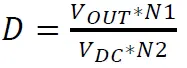
Load side
The resistive load is formulated based on the following equations for each of the converters:
POUT
DC power / real power at the load
D
Duty cycle as per section 6.2
Rout
Resistive load of the converter
n
Turns ratio (N2/N1)
Push-Pull (PP), Full Bridge (FB)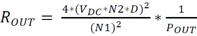 Half Bridge (HB)
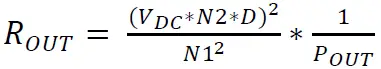
VALIDATION OF PLECS RESULTS WITH PSCAD
To ensure supplied simulation results are reliable, each of the Isolated DC-DC converter models (Push pull, Half-bridge, Full-bridge) is validated with another simulation platform or compared to real measurement data. The circuit topology is reconstructed in PSCAD to validate the results obtained from the SEMIS web simulation tool. The objective of the work is to develop an open-loop, Push-Pull, Half-Bridge and Full-Bridge converter models with loss and temperature estimation in PSCAD and to validate the steady-state results obtained through SEMIS simulation model using pulse-width modulation. The IGBT and Diode XML data which was created from the device datasheets for SEMIS simulations is modified to individual .txt files for switch turn-on energy (Eon), switch turn-off energy (E off), diode reverse recovery energy (Erec), the on-state voltage drop of IGBT (Vt), and on state voltage drop of the diode (Vd) at different temperatures, to make the data readable in PSCAD. The PSCAD and SEMIS circuit models are made as identical as possible to prevent any errors in validation due to the dissimilarities. Junction to Case and Case to Heat sink thermal resistances for the IGBT and Diode have been captured from the device datasheet while the Heat sink to ambient thermal resistance Rth(h-a) is assumed as 2K/kW with different ambient temperatures.
Five cases are simulated in PSCAD and SEMIS by varying different parameters like DC Voltage, Switching Frequency, Load Power, Heat Sink, etc. with the electrical parameters presented in the tables below for comparison.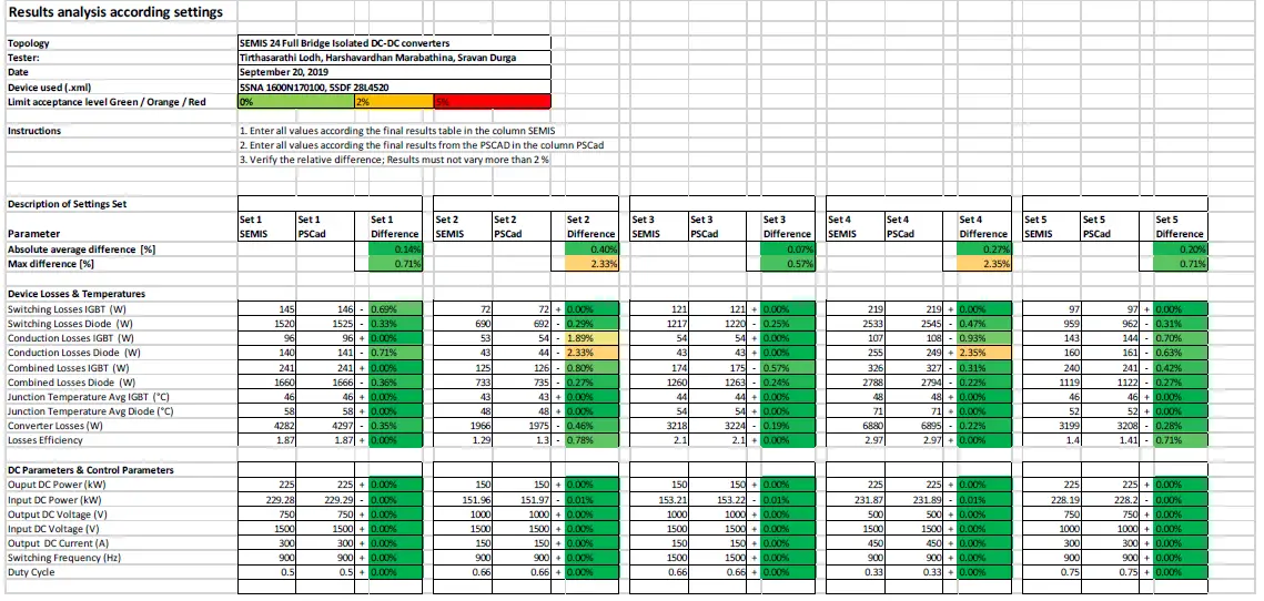 Validation results from comparison Full-Bridge Isolated DC-DC Converter
Validation of Plecs Results with PSCA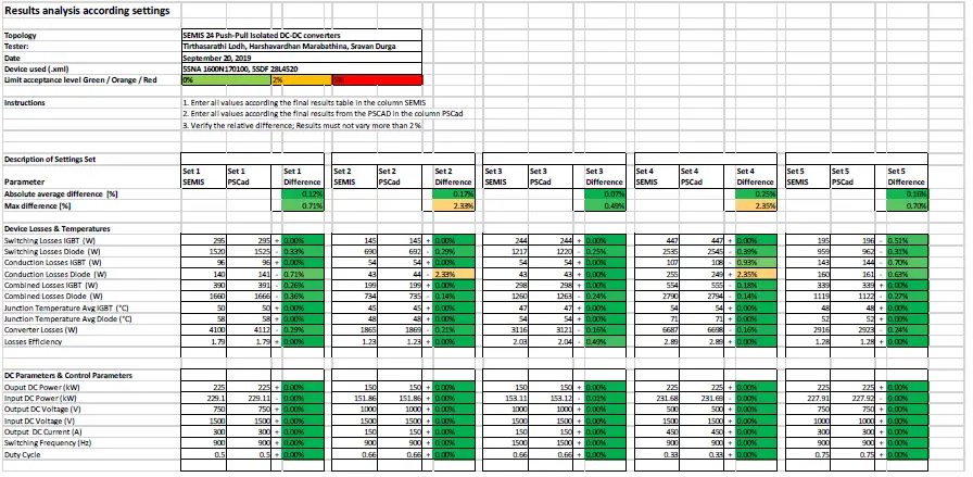 Validation results from comparison Push-pull Isolated DC-DC Converter
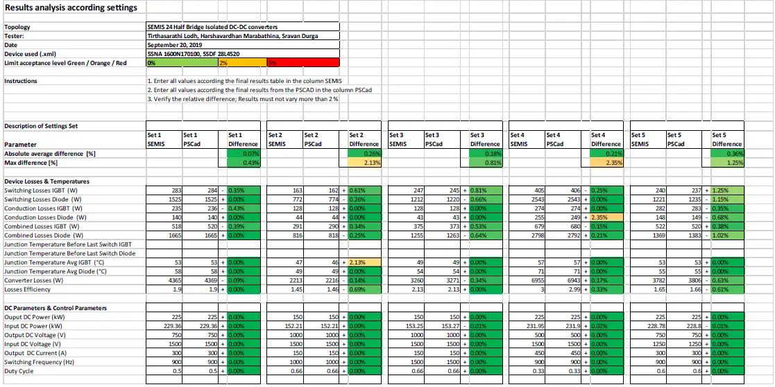 Validation results from comparison Half-Bridge Isolated DC-DC Converter
USER MANUAL REVISION HISTORY
| Rev. | Page | Change Description | Date / Initial |
| 1.0 | all | Initial version new design | 2019-12-06 PGGI/SD |
SIMULATION SOFTWARE RELEASE HISTORY
| Rev. | New topic | Fixed defects | Tvj influence | Date |
| 1.0 | Initial version | – | – | 2019-12-06 PGGI/SD |
Contact
ABB Power Grids Switzerland Ltd.
Semiconductors
Fabrikstrasse 3
5600 Lenzburg, Switzerland
Phone: +41 58 586 1419
Fax: +41 58 586 1306
E-Mail: [email protected]
abb.com/semiconductors
Note
We reserve the right to make technical changes or modify the contents of this document without prior notice. With regard to purchase orders, the agreed particulars shall prevail. ABB does not accept any responsibility whatsoever for potential errors or possible lack of information in this document. We reserve all rights in this document in the
subject matter and illustrations contained therein. Any reproduction- in whole or in parts- is forbidden without ABB’s prior written consent.


