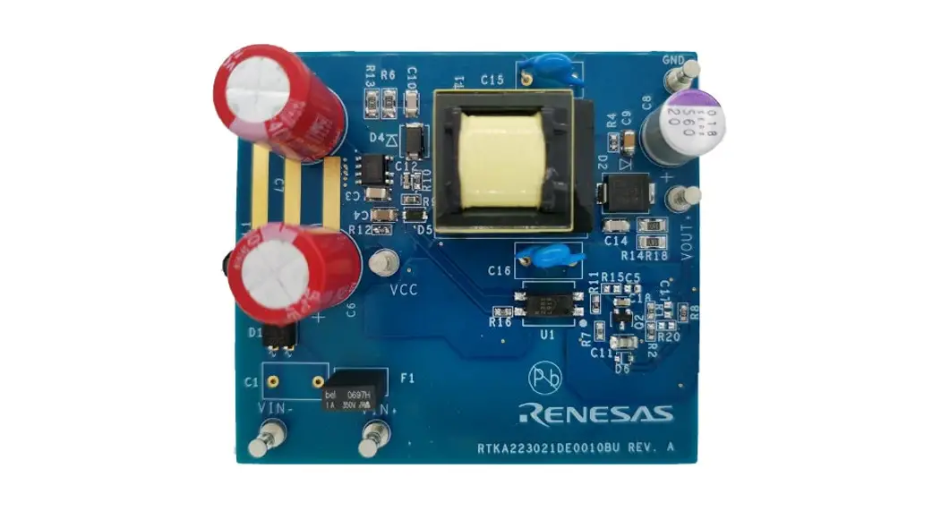
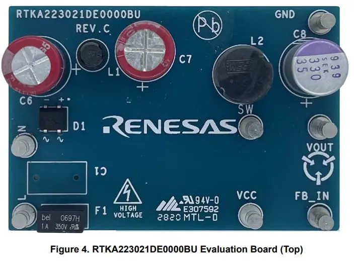
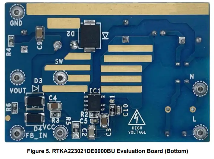
![]() RTKA223021DE0000BU High Voltage Buck Converter Evaluation Board
RTKA223021DE0000BU High Voltage Buck Converter Evaluation Board
Instruction Manual
RTKA223021DE0000BU High Voltage Buck Converter Evaluation Board
The RAA223021 evaluation board (RTKA223021DE0000BU) is a high voltage buck converter that demonstrates a low-cost high performance non-isolated AC/DC conversion from a universal input of 85VAC to 265VAC, to a 12V output with the output current up to 667mA.
The board has built-in overcurrent, short-circuit, input brownout, and over-temperature protection, and is designed on a single-side PCB with a full-wave input rectification. It is pre-compliant with conducted EMI requirements by EN55022/CISPR 22.
RTKA223021DE0000BU uses the RAA223021 SOIC-7 packaged IC.
Features
- Universal input
- Single side PCB with low-cost external components
- EMI compliance for EN55022/CISPR22
- Standby power less than 20mW
- No audible noise
Specifications
This board is optimized for the following operating conditions:
- Input voltage: 85VAC ~ 265VAC
- Output voltage: 12VDC
- Output current: 667mA max
- Output power: 8W
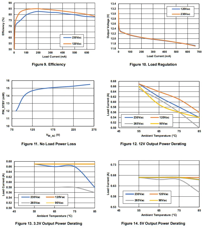
- Efficiency: >77% at 100% load; 80% at 50% load
- No-load power: 14mW at 120VAC; 16mW at 230VAC
- Load regulation: ±2.4%, load range 10% to 100%
- Operating temperature: -40~85°C
- Board dimension: 40mm x 60mm.
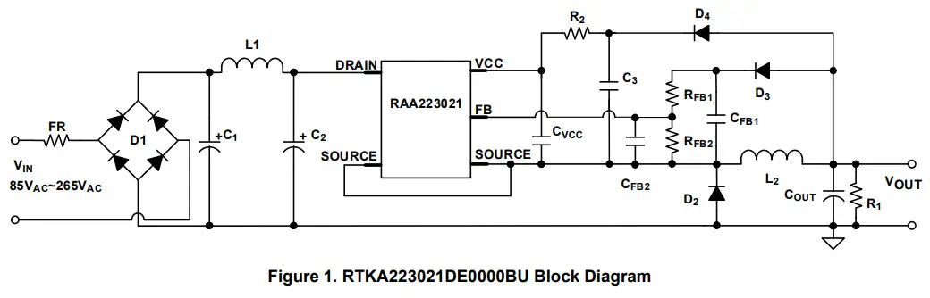
Table 1. HV Buck of 021 Power Derating at 85°C Ambient Temperature
| Output Setting Voltage (V) | 120VAc | 230VAc | 90VAc-265VAc |
| 3. | 0.67A | 0.58A | 0.56A |
| 5 | 0.67A | 0.66A | 0.6A |
| 9 | 0.64A | 0.6A | 0.56A |
| 12 | 0.56A | 0.54A | 0.5A |
| 15 | 0.56A | 0.52A | 0.5A |
| 24 | 0.49A | 0.5A | 0.46A |
Table 2. Component Selection Guide
| VOUT (V) | CFB1 (°F) | RFB1 (k12) | RFB2 (kO) | L2 (H) | R2 (kO) | R1 (Ito) |
| 24 | 100 | 397 | 45 | 1m | 30 | 100 |
| 15 | 100 | 397 | 77. | 1m | 10 | 47 |
| 12 | 47 | 397 | 99. | 680p | 10 | 47 |
| 9 | 100 | 397 | 142 | 470p | 5. | 47 |
| 5 | 200 | 100 | 82 | 330p | 100 | 10 |
| 3. | 200 | 100 | 180 | 330p | NC | 3 |
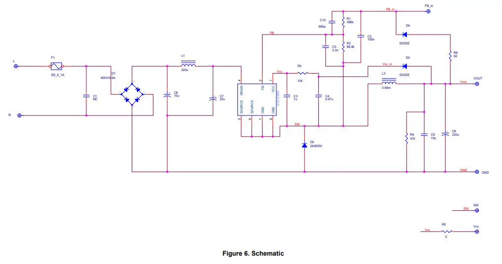
Functional Description
The RTKA223021DE0000BU is a buck regulator implemented with a high-side float-switching topology, with a switching frequency up to 43kHz. D1 is a full bridge rectifier on the input end. FR is a 1A fuse providing input overcurrent protection. As an option, you can replace the standard fuse with a fusible resistor instead to limit inrush current.
C1, L1, and C2 consist of the input filter that provides the energy buffer after rectification and reduces conducted EMI noises to the input. L2, D2, and COUT are the buck converter components. RFB1, RFB2, CFB2, and CFB1 provide the output feedback signal to the IC. D4 and R2 provide VCC biasing current after startup to increase efficiency. They can be optional for low-cost low-power applications. CVCC is the IC supply capacitor.
1.1 Recommended Equipment and Operating Range
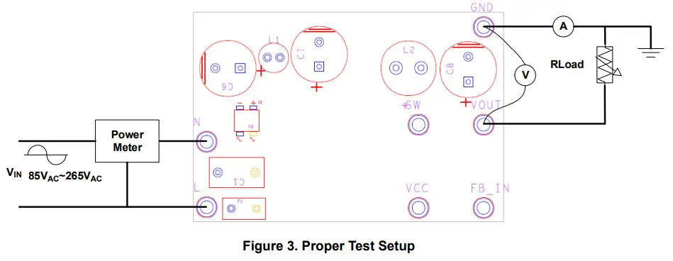
- AC Power supply capable of generating AC voltage from 85VAC to 265VAC at 60Hz/50Hz, with at least 100mA output current capability.
- Load resistor box with an adjustable value of 18Ω and up, or an electronics load that can emulate a resistor load or current load up to 667mA.
- Multi-meters to measure the output voltage and current.
- Power meter to measure the AC input power.
1.2 Setup and Configuration
- Program the AC power supply with a voltage between 85VAC and 265VAC at the corresponding frequency of 60Hz or 50Hz.
- While the AC power supply is off, connect the output cables of the AC power supply to the L and N terminal of the RTKA223021DE0000BU. An optional power meter can be added in between the AC power supply output and the input of the board.
- Connect the load to the output terminals VOUT and GND.
- Connect a voltage meter to VOUT and GND and connect a current meter between the board outputs and the load.
- Turn on the AC power supply.
Board Design
2.1 Layout Guidelines
Proper layout is important to ensure a stable operation, good thermal behavior, EMI performance, and reliable operation for various operating environments. Please pay attention to the following layout recommendations.
- Leave proper spacing (minimum1.4mm) between high voltage (max 400V) traces and low voltage traces.
- Keep a small loop from the input filter capacitor to IC, switching inductor, output capacitor, and to the ground of the input capacitor.
- Keep a small loop consisting of a switching inductor, output capacitor, and freewheeling diode.
- Keep a small loop consisting of an input filter capacitor to IC and a freewheeling diode.
- Keep sufficient copper area on the IC drain and/or source pin (not less than 140mm2 for 6-8W output power) for better thermal performance.
- Keep the switching inductor away from the input EMI inductor to avoid noise coupling, especially when an unshielded switching inductor is used.
- Keep a small loop from the input filter capacitor to IC, sample hold circuit, output capacitor, and to the ground of the input capacitor.
- Place the VCC decoupling cap and FB pin decoupling cap close to the pins.
2.2 Schematic Diagrams
2.3 Bill of Materials
| Qty | Reference Designator | Description | Manufacturer | Manufacturer Part |
| 1 | C2 | CAP CER 0.1pF 50V COG 1206 | TDK | CGA5L2COG1H104J160AA |
| 1 | C3 | CAP CER 1pF 25V X7R 1206 | TDK | CGJ5L2X7R1E105K160AA |
| 1 | C4 | CAP CER 0.47pF 50V X7R 1206 | TDK | C3216X7R1H474K160AA |
| 1 | C5 | CAP CER 2200pF 50V X7R 0603 | TDK | CGA3E2X7R1H222K080AA |
| 2 | C6 | CAP ALUM 10pF 20% 400V RADIAL | WE | 860021375011 |
| C7 | CAP ALUM 10pF 20% 400V RADIAL | WE | 860021375011 | |
| 1 | C8 | CAP ALUM POLY 330pF 20% 35V PH | Panasonic | 35SEK330M |
| 1 | C9 | CAP CER 10pF 25V X7R 1206 | TDK | C3216X7R1E106K160AB |
| 1 | C10 | CAP CER 680pF 50V COG 0603 | TDK | CGA3E2COG1H681J080AA |
| 1 | D1 | BRIDGE RECT 1P 600V 500mA MBM | N/A | MB6M |
| 1 | D2 | DIODE GEN PURP 600V 2A SMC | ST | STTH2R06S |
| 2 | D3 | DIODE GEN PURP 600V 1A SMA | ST | STTH1R06A |
| D4 | DIODE GEN PURP 600V 1A SMA | ST | STTH1 R06A | |
| 1 | Fl | FUSE BOARD MNT 1A 250VAc RADIAL | Eaton – Electronics Division | SS-5-1A |
| 1 | IC1 | 700V, 8W AC/DC Buck Regulator | Renesas | RAA223021 |
| 1 | L1 | FIXED IND 220pH 500MA 1.20 TH | WE | 7447462221 |
| 1 | L2 | FIXED IND 680pH 900MA 790m0 | WE | 7447480681 |
| 1 | R1 | RES 397k0 1%1110W 0603 | KOA | RN73H1JTTD3973F25 |
| 1 | R2 | RES 98.8k0 1% 1110W 0603 | KOA | RN73R1JTTD9882F25 |
| 1 | R3 | RES SMD 10k0 5% 1/10W 0603 | Panasonic | ERJ-3GEYJ103V |
| 1 | R4 | RES SMD 471(0 5% 1/10W 0603 | Yageo | RC0603JR-0747KL |
| 1 | R5 | RES 0 OHM JUMPER 1/4W 1206 | Stackpole Electronics Inc | RMCF1206ZTOROO |
| 1 | R6 | RES SMD 500 0.1% 1/10W 0603 | Yageo | RT0603BRE075ORL |
| 7 | TP | CONN-DBL TURRET, TH, 0.109LENGTH, BRASS/TIN, ROHS | Keystone Electronics | 1514-2 |
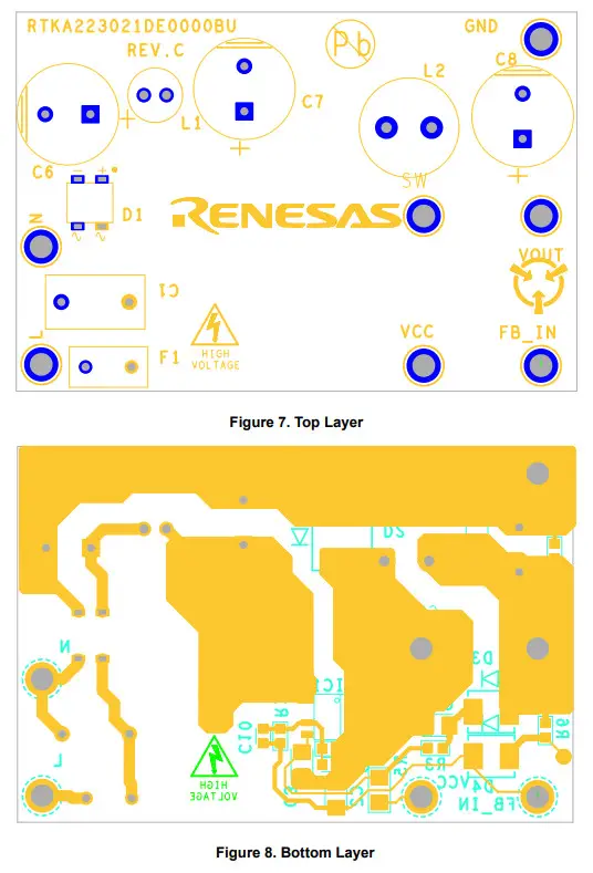
2.4 Board Layout
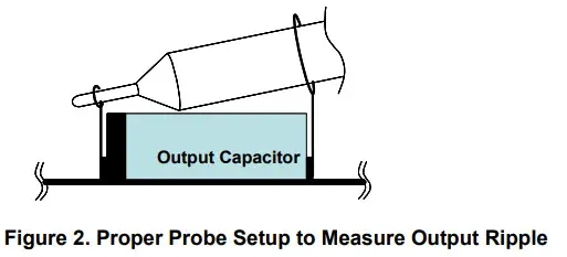
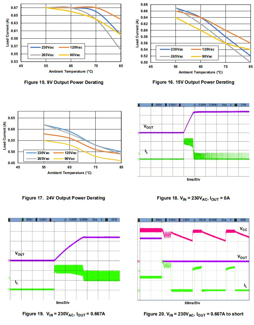
Typical Performance Graphs
VOUT = 12V, unless otherwise noted.
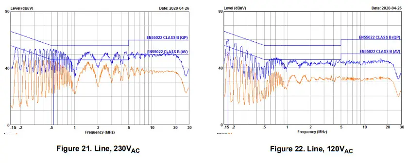
EMI Test Result
Conducted EMI compliance for EN55022/CISPR22 (12V/600mA output)
Ordering Information
| Part Number | Description |
| RTKA223021DE0000BU | High Voltage BUCK Converter Evaluation Board |
Revision History
| Revision | Date | Description |
| 1. | May 26, 2021 | Updated Tables 1 and 2 with 24V output. Added 24V Figures 17 and 18. |
| 1.0 | Mar 26, 2021 | Initial release |
IMPORTANT NOTICE AND DISCLAIMER
RENESAS ELECTRONICS CORPORATION AND ITS SUBSIDIARIES (“RENESAS”) PROVIDE TECHNICAL SPECIFICATIONS AND RELIABILITY DATA (INCLUDING DATASHEETS), DESIGN RESOURCES (INCLUDING REFERENCE DESIGNS), APPLICATION OR OTHER DESIGN ADVICE, WEB TOOLS, SAFETY INFORMATION, AND OTHER RESOURCES “AS IS” AND WITH ALL FAULTS, AND DISCLAIMS ALL WARRANTIES, EXPRESS OR IMPLIED, INCLUDING, WITHOUT LIMITATION, ANY IMPLIED WARRANTIES OF MERCHANTABILITY, FITNESS FOR A PARTICULAR PURPOSE, OR NON- INFRINGEMENT OF THIRD PARTY INTELLECTUAL PROPERTY RIGHTS.
These resources are intended for developers skilled in the art of designing Renesas products. You are solely responsible for (1) selecting the appropriate products for your application, (2) designing, validating, and testing your application, and (3) ensuring your application meets applicable standards, and any other safety, security, or other equirements. These resources are subject to change without notice. Renesas grants you permission to use these resources only for the development of an application that uses Renesas products. Other reproduction or use of these resources is strictly prohibited. No license is granted to any other Renesas intellectual property or to any third-party intellectual property. Renesas disclaims responsibility for, and you will fully indemnify Renesas and its representatives against, any claims, damages, costs, losses, or liabilities arising out of your use of these resources. Renesas’ products are provided only subject to Renesas’ Terms and Conditions of Sale or other applicable terms agreed to in writing. No use of any Renesas resources expands or otherwise alters any applicable warranties or warranty disclaimers for these products.
Corporate Headquarters
TOYOSU FORESIA, 3-2-24 Toyosu,
Koto-ku, Tokyo 135-0061, Japan
www.renesas.com
Trademarks
Renesas and the Renesas logo are trademarks of Renesas Electronics Corporation. All trademarks and registered trademarks are the property of their respective owners.
Contact Information
For further information on a product, technology, the most up-to-date version of a document, or your nearest sales office, please visit: www.renesas.com/contact/


