![]() USER’ S MANUAL
USER’ S MANUAL
A48 MAIN BOARD
482A4801
Printed in Taiwan 2000
A48 Main Board
INDEX
This user’ s manual describes the jumper setting of A48 Main Board. For detailed technical information, please refer to CDs attached with PC system unit.
All other registered and unregistered trademarks are trademarks of their respective holders
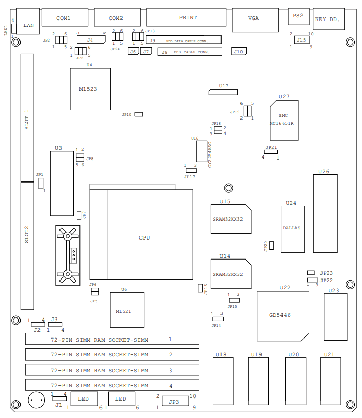
Jumpers Location Diagram for “A48” V2.X M/B
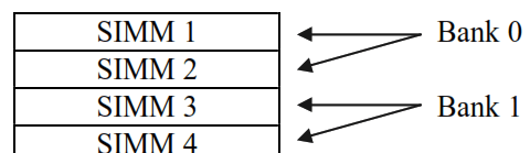
Memory configuration for “A48” V2.X main board
- System Memory’s Configuration.

The A48 mother board provides Auto-bank SIMM socket and supports 32-bit SIMM module operation. Install one 72-pin SIMM module in any of the four SIMM sockets will enable system to work.
Remark:
Please refer to above figure for SIMM socket. SIMM 1 and SIMM 2 stand for Bank 0, SIMM 3 and SIMM 4 stand for Bank 1.
Please make sure to install the same memory type at SIMM 1 and SIMM 2 for Bank 0, and same memory type at SIMM 3 and SIMM 4 for Bank 1. The memory won‘ t be recognized if different memory type installed at the same Bank. - VGA Memory’s Configuration.

VGA memory 1MB (EDO) U19 , U20 installed 2MB (EDO) U18 , U19 , U20 , U21 installed
IMPORTANT
The A48 on board PCI VGA ID is set on #31, if a PCI add-on cad to be installed, please set its ID at #1 -#30 to avoid conflict
Jumper settings
CPU selection: JP18 , JP5 , JP6 , JP8
| CPU | JP18 | JP5 | JP6 | JP8 |
| Intel Pentium 75 | 1-2 , 3-4 | off | off | 1-2 , 3-4 |
| Intel Pentium 90 | 1-2 | off | off | 1-2 , 3-4 |
| Intel Pentium 100 | 3-4 | off | off | 1-2 , 3-4 |
| Intel Pentium 120 | 1-2 | off | on | 1-2 , 3-4 |
| Intel Pentium 133 | 3-4 | off | on | 1-2 , 3-4 |
| Intel Pentium 150 | 1-2 , 3-4 | on | off | 1-2 , 3-4 |
| Intel Pentium 166 | 3-4 | on | on | 1-2 , 3-4 |
| Intel Pentium 200 | 3-4 | on | off | 1-2 , 3-4 |
| AMD 5k86-P75 | 1-2 , 3-4 | off | off | 1-2 , 3-4 |
| AMD 5k86-P90 | 1-2 | off | off | 1-2 , 3-4 |
| AMD 5k86-P100 | 3-4 | off | off | 1-2 , 3-4 |
| AMD 5k86-P133 | 3-4 | off | on | 1-2 , 3-4 |
Cache RAM size selection: JP14
| Cache RAM size | JP14 |
| 256KB (32Kb*32) | 2-3 |
| 512KB (64Kb*32) | 1-2 |
Keyboard Controller selection: JP10
| K/B Controller | JP10 |
| Built-in core logic | on |
| IC 8042 | off |
Reserved: JP3, JP4, JP7, JP15, JP17, JP22
Real Time Clock Controller selection: JP9
| RTC Controller | JP9 |
| Dallas 12887 | off |
| Built-in core logic | on |
Clean CMOS data (Dallas 12887 only): JP20
| RTC Controller | JP20 |
| Normal operation | off |
| Clean CMOS data | on |
ROM BIOS type selection: JP1
| ROM BIOS type | JP1 |
| +5V EPROM or Flash ROM | 2-3 |
| +12V Flash ROM | 1-2 |
DMA channel selection for ECP mode of Parallel Port: JP19
| DMA channel | JP19 |
| DMA 3 | 1-3 , 2-4 |
| DMA 1 | 3-5 , 4-6 |
The Pin 1 assignment of the connector of COM1: JP2
| Pin 1 signal | JP2 |
| *DCD1 | 1-2 |
| +5Vdc | 3-4 |
| +12Vdc | 5-6 |
The Pin 2 assignment of the connector of COM2: JP13
| Pin 1 signal | JP13 |
| *DCD2 | 1-2 |
| +5Vdc | 3-4 |
| +12Vdc | 5-6 |
USB headers: J2 , J3
| Pin # | Pin assignment |
| 1 | Vcc |
| 2 | USB data |
| 3 | USB data |
| 4 | GND |
IR header: JP21
| Pin # | Pin assignment |
| 1 | IR RX 2 |
| 2 | GND |
| 3 | IR TX 2 |
| 4 | Vcc |
Header for LAN slot: LAN1
Header for FAN: J6 , J7![]()


