Yealink YL430132 IEEE 802.11 a/b/g/n Wireless LAN and Bluetooth Combo Stamp Module
General Description
The YL430132 IEEE 802.11 a/b/g/n SDIO Wi-Fi with Bluetooth 5.0 combo stamp module is a highly integrated wireless local area network (WLAN) solution to let users enjoy the digital content through the latest wireless technology without using the extra cables and cords. It combines with Bluetooth 5.0 and provides a complete 2.4GHz Bluetooth system which is fully compliant to Bluetooth 5.0 with integrated PA for Class 1.5 and Low Energy (BLE) that supports EDR of 2Mbps and 3Mbps for data and audio communications. It enables a high performance, cost effective, low power, compact solution that easily fits onto the SDIO and UART stamp module.
Compliant with the IEEE 802.11a/b/g/n standard, YL430132 uses Direct Sequence Spread Spectrum (DSSS), Orthogonal Frequency Division Multiplexing (OFDM), BPSK, QPSK, CCK and QAM baseband modulation technologies.
A high level of integration and full implementation of the power management functions specified in the IEEE 802.11 standard minimize system power requirements by using YL430132. YL430132 module adopts BCM430132 single chip solution. The module design is based on the BCM430132 solution.
Key Features
- Single spatial stream up to a 72 Mbps data rate.
- 1(Transmit) ´1(Receive) Wi-Fi and Bluetooth 0
- Low power consumption and high performance
- Enhanced wireless security
- Supports Bluetooth 5.0-compliant features
- BDR、EDR(2′3Mbps)、LE(1Mbps) supported
Block Diagram
A simplified block diagram of the YL430132 module is depicted in the figure below.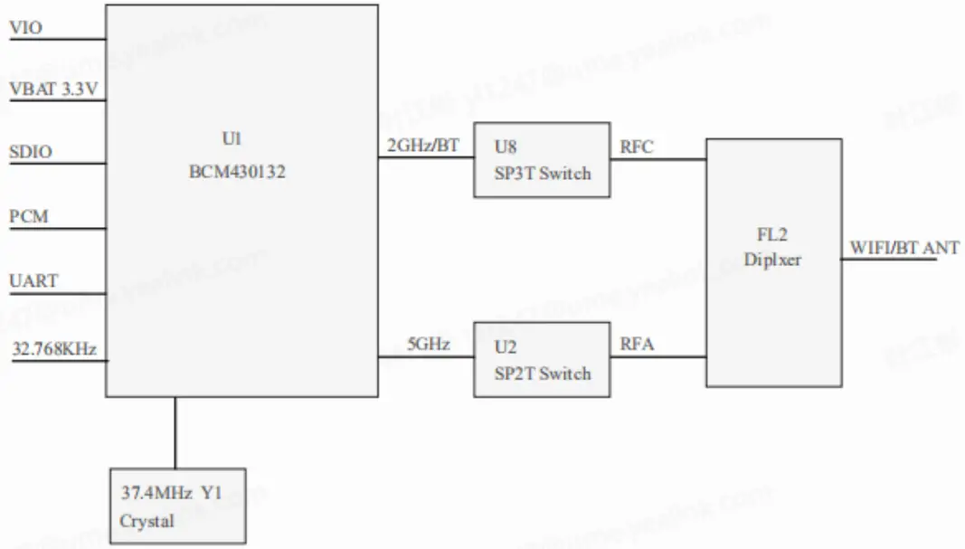
Specifications Table
| Model Name | YL430132 |
| Description | Wireless LAN &Bluetooth Stamp Module |
| WLAN Standard | IEEE 802.11a/b/g/n & Wi-Fi compliant |
| Bluetooth Standard | Bluetooth 2.1 + EDR, Bluetooth 3.0, Bluetooth 4.2 (Bluetooth Low Energy), and Bluetooth 5.0. |
| Major Chipset | BCM430132 |
| Host Interface | Wi-Fi: SDIO, BT: UART |
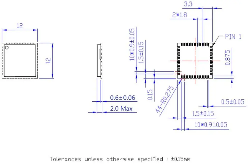
| Dimensions | 12mm * 12mm * 2.0mm |
| Wi-Fi VID/PID | TBD |
| BT VID/PID | TBD |
| Weight | TBD |
| Operating Conditions | |
| Voltage | power supply for host:3.3V |
| Temperature | -40℃~85℃ |
| Storage temperature | -45℃~135℃ |
| Electrical Specifications | |
| Frequency Range | WLAN: 2.4 GHz ISM Bands 2.4-2.4835 GHz 5Ghz: 5.15~5.35GHz、5.47~5.725GHz、5.725~5.85GHz (5GHz UNII Band) Bluetooth: 2402~2480MHz |
| Modulation | CCK、OFDM /64-QAM、16-QAM、QPSK、BPSK for WLAN GFSK, π/4-DQPSK, 8DPSK for Bluetooth |
| Output Power | WLAN: 802.11b: TBD dBm (11Mbps) 802.11g: TBD dBm (54Mbps) 802.11n @2.4GHz: TBD dBm (HT20 MCS7) 802.11a @5GHz: TBD dBm (54Mbps) |
| Receive Sensitivity | 802.11b: TBD dBm (11Mbps) 802.11g: TBD dBm (54Mbps) 802.11n @2.4GHz: TBD dBm (HT20 MCS7) 802.11a @5GHz: TBD dBm (54Mbps) BT: BER < 0.1% (IQXEL80 Tx -70 Bm) |
| Data Rates | WLAN 802.11b: 1, 2, 5.5, 11Mbps 802.11a/g: 6, 9, 12, 18, 24, 36, 48, 54Mbps 802.11n: up to 72Mbps-single Bluetooth BDR、EDR(2、3Mbps)、LE(1Mbps) |
| Security |
|
| Operating System Compatibility | TBD |
Electrical Characteristics
Absolute Maximum Ratings
| Symbol | Parameter | Maximum | Unit |
| VDD | 3.3V power supply voltage | 5.25 | V |
| VDDIO | Voltage supply for GPIO | 2.07 | V |
| RFin | Maximum RF input (reference to 50 Ω) | TBD | dBm |
Recommended Operating Conditions
| Symbol | Parameter | Rating | Unit |
| VDD | 3.3V power supply voltage | 3.2~5.0 | V |
| VDDIO | Voltage supply for GPIO | 1.62~1.98 | V |
GPIO DC Characteristics
| Symbol | Parameter | Minimum | Typical | Maximum | Unit |
| VIH | Input high voltage | 0.65*VDDIO | — | VIO+0.3 | V |
| VIL | Input low voltage | -0.3 | — | 0.35*0.65*VDDIO | V |
| VOH | Output high voltage | VDDIO-0.45 | — | VIO | V |
| VOL | Output low voltage | 0 | — | 0.45 | V |
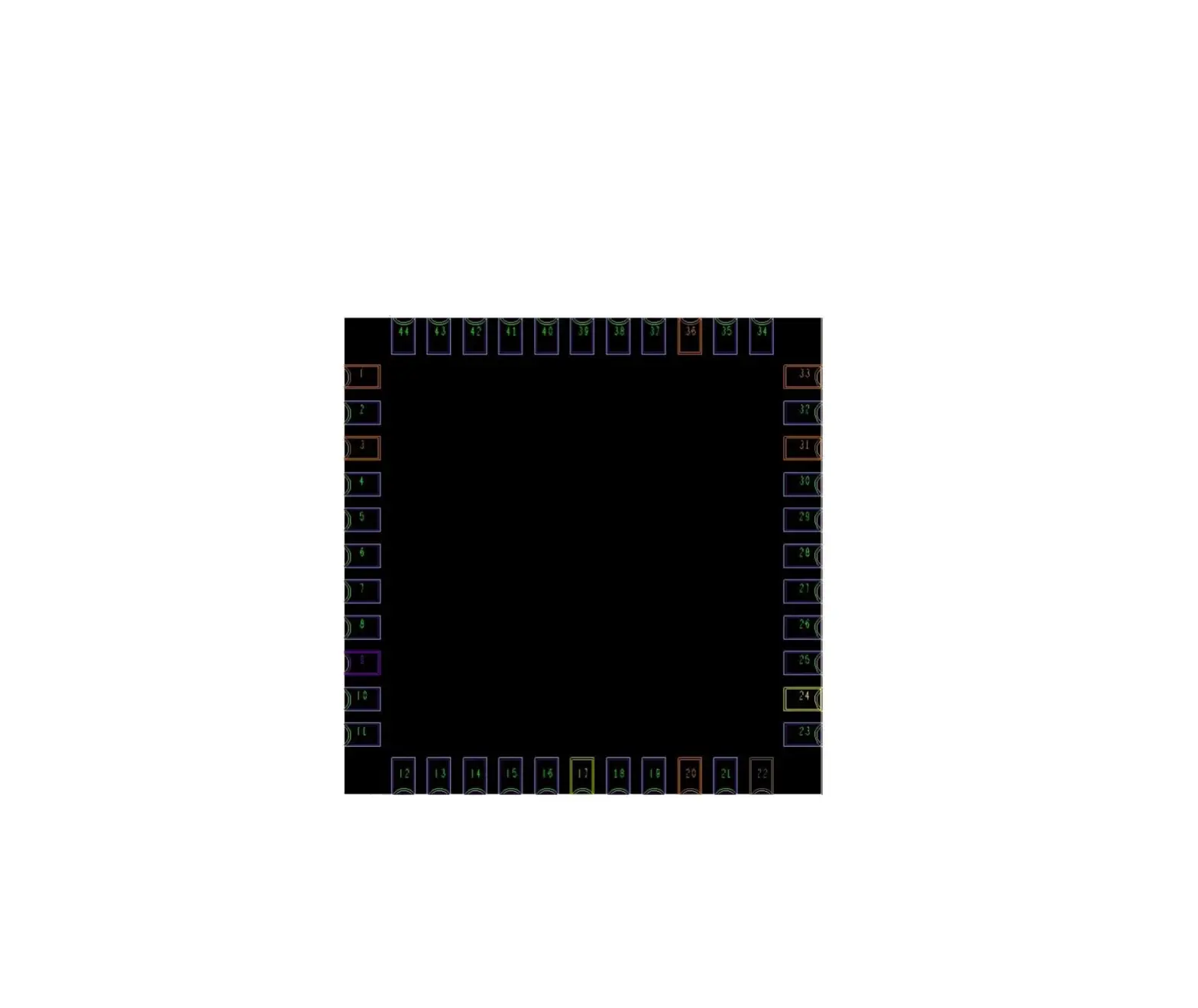
Pin Definition
Pin Description
| Pin No. | Definition | Basic Description Type | Type |
| 1 | GND | GROUND | GND |
| 2 | WL_BT_ANT | Wi-Fi/BT RF signal | I/O |
| 3 | GND | GROUND | GND |
| 4 | NC | Floating Pin, No connect to anything. | Floating |
| 5 | NC | Floating Pin, No connect to anything. | Floating |
| 6 | Host_Wakeup_BT | Host wakeup BT device | IN |
| 7 | BT_wakeup_Host | BT Device wakeup Host | I/O |
| 8 | NC/TMS | Reserve for EJTAG | I/O |
| 9 | VBAT | DC power supply +3.3V input | VCC |
| 10 | XTAL_IN/NC | Floating Pin, No connect to anything. | Floating |
| 11 | XTAL_OUT/NC | Floating Pin, No connect to anything. | Floating |
| 12 | WL_EN | GPIO pin to on/off the Wi-Fi function by software. Active high. Reserve pull high 100K resistor and shunt 100pF capacitor to GND on platform. | IN |
| 13 | WL_wakeup_Host | WLAN device wakeup host | OUT |
| 14 | SDIO_DATA2 | SDIO Data Line 2 | I/O |
| 15 | SDIO_DATA3 | SDIO Data Line 3 | I/O |
| 16 | SDIO_CMD | SDIO Command Input | I/O |
| 17 | SDIO_CLK | SDIO Clock Input | IN |
| 18 | SDIO_DATA0 | SDIO Data Line 0 | I/O |
| 19 | SDIO_DATA1 | SDIO Data Line 1 | I/O |
| 20 | GND | GROUND | GND |
| 21 | NC | Floating Pin, No connect to anything. | Floating |
| 22 | VDDIO | 1.8V-3.3V VDDIO supply for WLAN and BT | VCC |
| 23 | NC | Floating Pin, No connect to anything. | Floating |
| 24 | LPO | External low-power 32.768KHz clock input. | IN |
| 25 | PCM_OUT | PCM synchronous data output, connected to PCM_IN on the host. | OUT |
| 26 | PCM_CLK | PCM Clock | I/O |
| 27 | PCM_IN | PCM synchronous data input, connected to PCM_OUT on the host. | IN |
| 28 | PCM_SYNC | PCM synchronous data SYNC | I/O |
| 29 | TDI | Reserve for EJTAG | IN |
| 30 | TDO | Reserve for EJTAG | OUT |
| 31 | GND | GROUND | GND |
| 32 | TCK | Reserve for EJTAG | GND |
| 33 | GND | GROUND | GND |
| 34 | BT_EN | GPIO pin to on/off the BT function by software. Active high. Reserve pull high 100K resistor and shunt 100pF capacitor to GND on host. | IN |
| 35 | NC | Floating Pin, No connect to anything. | Floating |
| 36 | GND | GROUND | GND |
| 37 | NC | Floating Pin, No connect to anything. | Floating |
| 38 | NC | Floating Pin, No connect to anything. | Floating |
| 39 | NC | Floating Pin, No connect to anything. | Floating |
| 40 | NC | Floating Pin, No connect to anything. | Floating |
| 41 | UART_RTS | UART Ready To Send, connected to CTS on the host. | OUT |
| 42 | UART_TXD | UART Transmit Data, connected to RXD on the host. | OUT |
| 43 | UART_RXD | UART Receive Data, connected to TXD on the host. | IN |
| 44 | UART_CTS | UART Clear To Send, connected to RTS on the host. | IN |
FCC regulatory compliance statement
§15.19 Statement
This device complies with Part 15 of the FCC Rules. Operation is subject to the following two conditions: (1) this device may not cause harmful interference, and (2) this device must accept any interference received, including interference that may cause undesired operation.
§15.21 Information to user
Warning: changes or modifications not expressly approved by the party responsible for compliance could void the user’s authority to operate the equipment.
- List of applicable FCC rules:
47 CFR Part 15, Subpart C 15.247
47 CFR Part 15, Subpart E 15.407 - Summarize the specific operational use conditions
The module can be used in teleconference machine. After installing this module, the telephone can be connected to the router through a wireless network. In WIFI coverage, users can send various instructions through smart phones or PCs, which is very convenient. The input voltage of the module is nominally 5V, and other antennas of the same type with less than the original gain can be replaced. - Limited module procedures
This module is a limited module. - Trace antenna designs
The antenna is not a trace antenna. - RF exposure considerations
This Module complies with FCC radiation exposure limits set forth for an uncontrolled environment. This equipment should be installed and operated with a minimum distance of 20cm between the radiator and your body. This transmitter must not be co-located or operating in conjunction with any other antenna or transmitter. - Antennas
The module itself does not have an antenna. During the test, the host provides a PCB antenna with a maximum gain of 3dBi.
If you desire to increase antenna gain and either change antenna type or use same antenna type certified, a Class II permissive change application is required to be filed by us, or you (host manufacturer) can take responsibility through the change in FCC ID (new application) procedure followed by a Class II permissive change application - Label and compliance information
Please notice that if the FCC identification number is not visible when the module is installed inside another device, then the outside of the device into which the module is installed must also display a label referring to the enclosed module. This exterior label can use wording such as the following: “Contains FCC ID: T2C-YL430132” any similar wording that expresses the same meaning may be used.
§ 15.19 Labelling requirements shall be complied on end user device.
Labelling rules for special device, please refer to §2.925, § 15.19 (a)(5) and relevant KDB publications. For E-label, please refer to §2.935. - Information on test modes and additional testing requirements
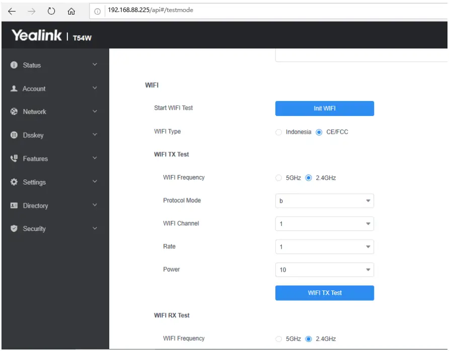
Test software access to different test modes: Wifi Test Tool v1.4.0
Testing item, Frequencies, Transmit Power, Modulation Type, test Antennas can be selected on the test script instructions.
- Additional testing, Part 15 Subpart B disclaimer
This modular transmitter is only FCC authorized for the specific rule parts listed on our grant, host product manufacturer is responsible for compliance to any other FCC rules that apply to the host not covered by the modular transmitter grant of certification.
Host manufacturer in any case shall ensure host product which is installed and operating with the module is in compliant with Part 15B requirements.
Please note that For a Class B or Class A digital device or peripheral, the instructions furnished the user manual of the end-user product shall include statement set out in §15.105 Information to the user or such similar statement and place it in a prominent location in the text of host product manual. Original texts as following:
For Class B
Note: This equipment has been tested and found to comply with the limits for a Class B digital device, pursuant to part 15 of the FCC Rules. These limits are designed to provide reasonable protection against harmful interference in a residential installation. This equipment generates, uses and can radiate radio frequency energy and, if not installed and used in accordance with the instructions, may cause harmful interference to radio communications. However, there is no guarantee that interference will not occur in a particular installation. If this equipment does cause harmful interference to radio or television reception, which can be determined by turning the equipment off and on, the user is encouraged to try to correct the interference by one or more of the following measures:
- Reorient or relocate the receiving antenna.
- Increase the separation between the equipment and receiver.
- Connect the equipment into an outlet on a circuit different from that to which the receiver is connected.
- Consult the dealer or an experienced radio/TV technician for help.
For Class A
Note: This equipment has been tested and found to comply with the limits for a Class A digital device, pursuant to part 15 of the FCC Rules. These limits are designed to provide reasonable protection against harmful interference when the equipment is operated in a commercial environment. This equipment generates, uses, and can radiate radio frequency energy and, if not installed and used in accordance with the instruction manual, may cause harmful interference to radio communications. Operation of this equipment in a residential area is likely to cause harmful interference in which case the user will be required to correct the interference at his own expense.
SED compliance statement
This device contains licence-exempt transmitter(s)/receiver(s) that comply with Innovation, Science and
Economic Development Canada’s licence-exempt RSS(s). Operation is subject to the following two conditions:
(1) This device may not cause interference.
(2) This device must accept any interference, including interference that may cause undesired operation of the device.
ISED Radiation Exposure statement
This equipment complies with IC RSS-102 radiation exposure limits set forth for an uncontrolled environment.
This equipment should be installed and operated with minimum distance 20cm between the radiator and your body.
End Device Labelling
Please notice that if the IC identification number is not visible when the module is installed inside another device, then the outside of the device into which the module is installed must also display a label referring to the enclosed module. This exterior label can use wording such as the following: “Contains IC: 10741A-YL430132” any similar wording that expresses the same meaning may be used.
5G Wi-Fi Use Notice
- the device for operation in the band 5150-5250 MHz is only for indoor use to reduce the potential for harmful interference to co-channel mobile satellite systems;
- the maximum antenna gain permitted for devices in the bands 5250-5350 MHz and 5470-5725 MHz shall comply with the e.i.r.p. limit; and
- the maximum antenna gain permitted for devices in the band 5725-5825 MHz shall comply with the e.i.r.p. limits specified for point-to-point and non point-to-point operation as appropriate.
- Users should also be advised that high-power radars are allocated as primary users (i.e. priority users) of the bands 5250-5350 MHz and 5650-5850 MHz and that these radars could cause interference and/or damage to LE-LAN devices.
This radio transmitter [IC: 10741A-YL430132] has been approved by Innovation, Science and Economic
Development Canada to operate with the antenna types listed below, with the maximum permissible gain indicated. Antenna types not included in this list that have a gain greater than the maximum gain indicated for any type listed are strictly prohibited for use with this device. a list of all antenna types
| PCB Antenna | 3dBi |


