![]()
WiFi/BT Combo Module
Model: SBW-M3
Product Specification
| Designed by | Checked by | Approved by |
Revision Record
| Rev. No | Date | Item | Modifications | Approved |
Federal Communication Commission Interference Statement
This device complies with Part 15 of the FCC Rules. Operation is subject to the following two conditions:
- This device may not cause harmful interference, and
- this device must accept any interference received, including interference that may cause undesired operation
This equipment has been tested and found to comply with the limits for a Class B digital device, pursuant to Part 15 of the FCC Rules. These limits are designed to provide reasonable protection against harmful interference in a residential installation. This equipment generates, uses, and can radiate radio frequency energy and, if not installed and used in accordance with the instructions, may cause harmful interference to radio communications. However, there is no guarantee that interference will not occur in a particular installation. If this equipment does cause harmful interference to radio or television reception, which can be determined by turning the equipment off and on, the user is encouraged to try to correct the interference by one of the following measures:
- Reorient or relocate the receiving antenna.
- Increase the separation between the equipment and receiver.
- Connect the equipment into an outlet on a circuit different from that to which the receiver is connected.
- Consult the dealer or an experienced radio/TV technician for help. FCC Caution: Any changes or modifications not expressly approved by the party responsible for compliance could void the user’s authority to operate this equipment. This transmitter must not be co-located or operating in conjunction with any other antenna or transmitter.
Radiation Exposure Statement:
This equipment complies with FCC radiation exposure limits set forth for an uncontrolled environment. This equipment should be installed and operated with a minimum distance of 20cm between the radiator & your body.
This device is intended only for OEM integrators under the following conditions:
- The antenna must be installed such that 20 cm is maintained between the antenna and users, and
- The transmitter module may not be co-located with any other transmitter or antenna.
As long as the 2 conditions above are met, further transmitter tests will not be required. However, the OEM integrator is still responsible for testing their end-product for any additional compliance requirements required with this module installed
IMPORTANT NOTE: In the event that these conditions can not be met (for example certain laptop configurations or co-location with another transmitter), then the FCC authorization is no longer considered valid and the FCC ID can not be used on the final product. In these circumstances, the OEM integrator will be responsible for re-evaluating the end product (including the transmitter) and obtaining a separate FCC authorization
End Product Labeling
This transmitter module is authorized only for use in devices where the antenna may be installed such that 20 cm may be maintained between the antenna and users. The final end product must be labeled in a visible area with the following: “Contains FCC ID: WF5SBWM3”. The grantee’s FCC ID can be used only when all FCC compliance requirements are met.
Manual Information To the End-User
The OEM integrator has to be aware not to provide information to the end-user regarding how to install or remove this RF module in the user’s manual of the end product which integrates this module. The end-user manual shall include all required regulatory information/warnings as shown in this manual
ISED Canada (IC) Statement
This Class B digital apparatus complies with Canadian ICES-003.
This device complies with Industry Canada licence-exempt RSS standard(s). Operation is subject to the following two conditions:
- this device may not cause interference, and
- this device must accept any interference, including interference that may cause undesired operation of the device.
RF Radiation Exposure Statement:
This equipment complies with IC radiation exposure limits set forth for an uncontrolled environment. This equipment should be installed and operated with a minimum distance of 20 centimeters between the radiator and your body
Required end product labeling:
Any device incorporating this module must include an external, visible, permanent marking or label that states: “Contains IC: 9080A-SBWM3”
This radio transmitter (identify the device by certification number or model number if Category II) has been approved by Industry Canada to operate with the antenna types listed below with the maximum permissible gain indicated. Antenna types not included in this list, having a gain greater than the maximum gain indicated for that type, are strictly prohibited for use with this device.
Overview
- Antenna Specification
(1) Bluetooth Antenna
(2) WiFi Antenna - Description:
(1) Electrical Characteristics
(2) Pin Map - RF Specifications
(1) Bluetooth RF Specifications
(2) WiFi RF Specifications - Certification Information
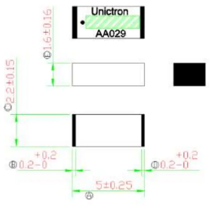
Antenna specification
(1) Bluetooth Antenna
1) Electrical specification
| Frequency range | 2.4 GHz band | |
| 2 400 MHz | 2 485 MHz | |
| VSWR | 2.5: 1 | 3.5: 1 |
| Peak Gain [dBi] | 2.03 | 0.85 |
| Impedance | 50 Ω | |
| Polarization | Linear | |
2) Mechanical specification
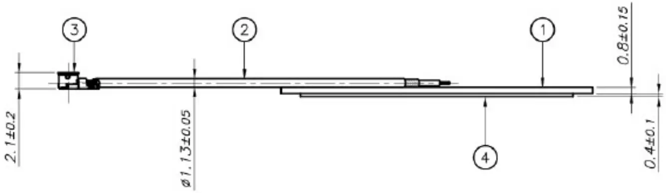
(2) WiFi Antenna
1) Electrical specification
| Frequency range | 2.4 GHz band | |
| 2 400 MHz | 2 485 MHz | |
| VSWR | 2.5: 1 | 3.5: 1 |
| Peak Gain [dBi] | 2.81 | 2.25 |
| Impedance | 50 Ω | |
| Polarization | Linear | |
| Frequency range | 5 GHz band | |
| 5 150 MHz | 5 875 MHz | |
| VSWR | 2.5: 1 | 3.5: 1 |
| Peak Gain [dBi] | 3.52 | 4.60 |
| Impedance | 50 Ω | |
| Polarization | Linear | |
2) Mechanical specification
Description
(1) Electrical Characteristics
| Parameter | Min | Typ. | Max | Unit |
| Supply Voltage | 3.0 | 3.3 | 4.8 | V |
| Storage Temperature | -40 | 25 | 125 | ℃ |
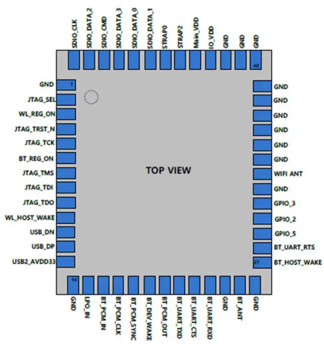
(2) Pin Map
| Pin Na | Pin Name | Desolation | Pad Woe |
| 1 | GND | Common Ground | |
| 2 | JTAG_SEL | 8i-directional | |
| 3 | WL_REG ON | WLAN Power-On Reset | Input |
| 4 | JTAG TFtST_N | Si-directional | |
| 5 | JTAG TCK | Bi-directional | |
| 6 | BT REG ON | Bluetooth Power-On Reset | Input |
| 7 | JTAG_TMS | 8i-directional | |
| 8 | JTAGTDI | Bi-directional | |
| 9 | JTAG TOO | Programmable input/output line | Bi-directional |
| 10 | WL_HOST WAKE | CMOS Output | |
| 11 | USI3DM | US$ Data minus | 8i-directional |
| 12 | USB DP | USB Data Plus | 8i-directional |
| 13 | US82 AVD033 | Bi-directional | |
| 14 | GND | Common Ground | |
| 15 | LP0_32768 | Low Power Oscillator | CMOS Input |
| 16 | BT PCMIN | Synchronous Data Input | CMOS input |
| 17 | BT_PCM CLK | Synchronous Data Clock | Bi-directional |
| 18 | BT PCM SYNC | Synchronous Data Sync | 8i-directional |
| 19 | BT DEV WAKE | Host to wake Bluetooth | CMOS Input |
| 20 | BT_PCM_OUT | Synchronous Data Output | CMOS Output |
| 21 | BT_UART TXD | UART Data Output | Si-directional |
| 22 | BT DART CTS | Si-directional | |
| 23 | I3T_UART RDX | UART Data Input | CMOS input |
| 24 | GND | Common Ground | |
| 25 | ST ANT | Bluetooth Antenna | RF |
| 26 | GND | Common Ground | |
| 27 | BT HOST WAKE | Bluetooth to wake the host | CMOS Output |
| 28 | BT_UART RTS | CMOS input |
| Pin No. | Pin Name | Description | Pad Type |
| 29 | GPIOS | Programmable input/output line | Bi-directional |
| 30 | GP102 | Programmable input/output line | Bi-directional |
| 31 | GPIO3 | Programmable input/output line | Bidirectional |
| 32 | GNO | Common Ground | |
| 33 | 11V1F1 ANT | WIFI Antenna | RF |
| 34 | GND | Common Ground | |
| 35 | GM) | Common Ground | |
| 36 | GND | Common Ground | |
| 37 | GND | Common Ground | |
| 38 | GND | Common Ground | |
| 39 | GND | Common Ground | |
| 40 | GND | Common Ground | |
| 41 | GO | Common Ground | |
| 42 | GND | Common Ground | |
| 43 | 10 VDD | Input/Cul:W(1O Port) Power 1.8V | Power |
| IL | Main VOID | Main Power 3.3V | Power |
| 45 | STRAP_2 | ||
| 46 | STRAP 0 | ||
| 47 | SDIO DATA 1 | SDIO V3.0 data line 1 | Bi-directional |
| 48 | SDIO DATA 0 | SDIO V3.0 data line C | Bi-directional |
| 49 | SDIO DATA 3 | SDIO V3.0 data line 3 | Bi-directional |
| SC | SDIO CMO | SD* V3.0 common line | Bi-directional |
| Si | SDIO DATA 2 | SDIO V3.0 data line 2 | Bi-directional |
| 52 | SDIO CLX | SDIO V3.0 clock line | Bi-directional |
RF Specifications
(1) Bluetooth RF Specifications
Bluetooth Receiver RF Specifications
| Parameter | Min | Typ | Max | Unit | |
| Frequency Range | 2L02 | 2480 | MHz | ||
| RX sensitivity | GFSK0.1%BERIMbps | -88 | -93.5 | dBm | |
| st/4-DQPSK 0.01% BER 2Mbps | –88 | -93.5 | |||
| 8-DPSK law% BER 3Mbps | –80 | _89.5 | |||
| C/I co-channel | GFSK. 0.1% | 11 | dB | ||
| TE/4-DC2SK 0.1% | 13 | ||||
| 8-DPSK 0.1% | 21 | ||||
| C/I 1MHz ADJ. Ch. | GFSK. 0.1% | 0 | |||
| rt/4-DQPSK. 0.1% | 0 | ||||
| 8-DPSK 0.1% | 5 | ||||
| C/I 2MHz ADJ. Ch. | GFSK. 0.1% | -30 | |||
| rt/4-DOPSK. 0.1% | -30 | ||||
| 8-DPSK 0.1% | -25 | ||||
| CA 23MHz ADJ. Ch. | GFSK. 0.1% | -40 | |||
| 11/4-DCPSK 0.1% | -40 | ||||
| 8-DPSK 0.1% | -33 | ||||
| C/1 image channel | G:SK 0.1% | -9 | |||
| rt/h-DoOPSK. 0.1% | -7 | ||||
| 8-DPSK 0.1% | 0 | ||||
| Snow Emissions | 30MHz | -95 | -62 | dBm | |
| 1 | -70 | -47 | |||
| 851 | -147 | ||||
| 925 | -147 | ||||
| 1805 | -147 | ||||
| 1930 | -147 | ||||
| 2110 | -147 | ||||
Bluetooth Transmitter RF Specifications
| Parameter | Min | Typ | Max | Unit | |
| Frequency Range | 2402 | 2480 | MHz | ||
| TX sensitivity | -4 | 2 | 6 | dBm | |
| Power Control step | 4 | dB | |||
| 20dB bandwidth | 960 | 1000 | MHz | ||
| Out-of Band Spurious Emissions | 30MHz – 1GHz | -36 | dBm | ||
| 1GHz-12 75GHz | -30 | ||||
| 1.8GHz-5 3GHz | -47 | ||||
| 5.1GHz – 5.3GHz | -47 | ||||
Local Oscillator Performance
| Parameter | Min | Typ | Max | Unit | |
| Initial Carrier Frequency Tolerance | +25 | +75 | MHz | ||
| Frequency Drift | DH1 packet | +8 | ±25 | kHz | |
| DH3 packet | +8 | ±40 | |||
| DH5 packet | +8 | ±40 | |||
| Drift rate | 5 | 20 | kHz/50us | ||
BLE RF Specifications
| Parameter | Min | Typ | Max | Unit | |
| Frequency Range | 2402 | 2480 | MHz | ||
| TX sensitivity | 8.5 | dBm | |||
| RX sense | -92 | -95.5 | dBm | ||
| Mod Char. | Delta Fl average | 225 | 255 | 275 | kHz |
| Delta F2 average | 230 | ||||
| Ratio | 0.8 | 1 00 | |||
Note: The above-mentioned values may vary depending on the circuit, in which this component is actually incorporated. You are, therefore, kindly requested to test the performance of this component t incorporated in your set.
(2) WiFi RF Specifications
2.4GHz Band RF Specifications
2.4GHz Switch time specifications
| Item | Min | Typ | Max | Unit |
| TX/RX Switch time | 5 | us | ||
| RX/TX Switch time | 2 | Us | ||
| Power-up and power-down ramp time | ∠2 | us |
WLAN 2 4GHz Receiver Performance Specifications
| Parameter | Condition/Notes | Min | Typ | Max | Unit |
| Frequency range | – | 240C | – | 25C0 | MHz |
| RX sensitivity IEEE 802.11b (8% PER for 1024 octet PSDU) | 1 Mbps DSSS | – | -98.4 | – | dBm |
| 2 Mbps DSSS | – | -95.7 | – | dBm | |
| 5.5 Mbps DSSS | – | -94.1 | – | dBm | |
| 11 Mbps DSSS | -90.4 | – | dBm | ||
| RX sensitivity IEEE 802. iig (10% PER for 1024 octet PSDU) | 6 Mbps OFDM | – | -95.0 | – | dBm |
| 9 Mbps OFDM | – | -94.3 | – | dBm | |
| 12 Mbps OFDM | – | -93.5 | – | dBm | |
| 18 Mbps OFDM | – | -90.6 | – | dBm | |
| 24 Mbps OFDM | – | -87.4 | – | dBm | |
| 36 Mbps OFDM | – | -84.1 | – | dBm | |
| 48 Mbps OFDM | – | -79.3 | – | dBm | |
| 54 Mbps OFDM | – | -77.9 | – | dBm | |
| RX sensitivity IEEE 802.11n (10% PER for 4096 octets PSDU) I Defined for default parameters: 800 ns GI and non-STBC. | 20 MHz channel spacing for all MCS rates | ||||
| MCSO | – | -94.5 | – | dBm | |
| MCS1 | – | -91.9 | – | dBm | |
| MCS2 | – | -90.1 | – | dBm | |
| MCS3 | -89.5 | – | dBm | ||
| MCS4 | – | -83.0 | – | dBm | |
| MCS5 | – | -78.3 | – | dBm | |
| MCS6 | – | -76.4 | – | dBm | |
| MCS7 | -74.4 | – | dBm | ||
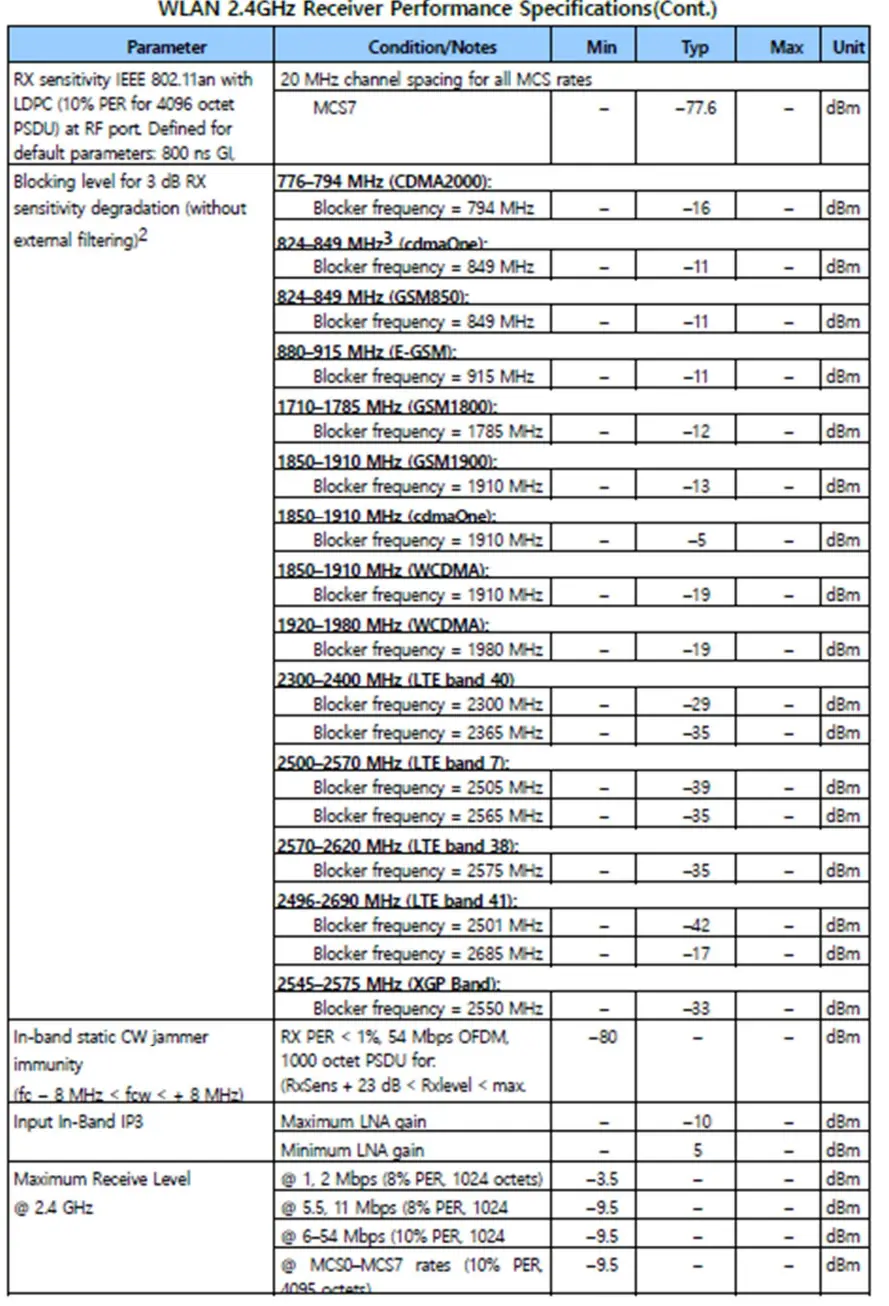
MAN 2.4GHz Receiver Performance Specifications(Cont.)
| Parameter | Condition/Notes | Min | Typ | Max I | Unit | |
| Adjacent channel rejection–DSSS 1Difference between interfering and the desired signal at 8% PER for 1024: octet PSDU with the desired signal level of specified ii Condition/Notes) | Desired and interfering signal 30 MHz apart | |||||
| 1 Mbps DSSS | -74 dBm | 35 | – | – | dB | |
| 2 PAbps C6SS | -74 dem | 35 | – | – | ||
| Desired and interfering signal 25 MHz apart | ||||||
| Si Mbps | -70 dBm | 35 | – | – | d8 | |
| 11 Mbps OFDM | -70 dem | 35 | – | – | d3 | |
| Adjacent channel rejection-OFOM I Difference ben, en interfering ar d desired signal (25 MH: apart) at 10% PER for 1024 octet PSC() with desired sign level as specified in Condition/ | 6 Mbps OFDM | -79 d8m | 16 | – | – | c13 |
| 9 Mbps OFOM | -78 dem | 15 | – | – | dB | |
| 12 Mbps OFDM | -76 dem | 13 | – | – | dB | |
| 18 Mbps OFOM | -74 dBm | 11 | – | – | dB | |
| 24 lips OFDM | -71 dBm | 8 | – | – | dB | |
| 36 Mbps OFOM | -67 dern | 4 | – | – | dB | |
| 48 Webs OFDM | -63 d8m | 0 | _ | – | dB | |
| 54 Mbps OFOM | -62 dBm | -1 | – | – | dB | |
| Adjacent channel rejection MCSO- MCS7 Difference between interfering and desired signal (25 MI-_ apart) at 10% PER for 4096 octet PSDU with desired signal level as specified in Condition/Notes) | MCCOY | -79 dBm | 16 | – | – | dB |
| MCS1 | -76 dem | 13 | – | – | dB | |
| MCS2 | -74 dBm | 11 | – | – | dB | |
| MCS3 | -71 dBm | 8 | – | – | dB | |
| PitCS4 | -67 dem | 4 | – | – | dB | |
| MCSS | -63 dBm | 0 | – | – | dB | |
| MCS6 | -62 dBm | -1 | – | – | dB | |
| MCS7 | -61 dBm | -2 | – | – | dB | |
| Ma: Ocimum receiver gain | – | – | – | 70 | – | dB |
| Gain control step | – | – | – | 3 | – | dB |
| RSSI acctracy4 | Rzrinoi -9S5 dRrri to -30 dBm | -5 | – | 5 | dB | |
| The range above -30 dBm | -8 | – | 8 | dB | ||
| Return loss | Zo = 50Ω across the dynamic | -10 | 11.5 | 13 | dB | |
| Receiver cascaded noise figure | At maximum gain | – | 4 | 11.5 | dB | |
WLAN 2.4GHz Transmitter Performance Specifications
| Parameter | Condition/Notes | Min | Typ | Max | Unit | ||
| Frequency range | – | 2400 | – | 2500 | MHz | ||
| Transmitted power in cellular and bands (at +21 t 100% duty cycle 1 Mbps CCIO 1 | 776-794 MHz (CDMA2000) | – | -164 | – | dBm/Hz | ||
| 869-960 MHz(cdmaOne) | – | -163 | – | dBm/Hz | |||
| 1450-1495 (DAB) | – | -153.6 | – | dBm/Hz | |||
| 1570-1580 MHz (GPS) | – | -1512 | – | dBm/Hz | |||
| 1592-1610 MHz (GLONASS) | – | -1504 | – | d8m/Hz | |||
| 1710-1800 (05C-1800-Uplink) | – | -145 | – | dBm/Hz | |||
| 1805-1893 Mit (GSM 1800) | – | -139 | – | d8m/Hz | |||
| 1850-1910 MHz (GSM 1900) | – | -139 | – | d8m/Hz | |||
| 1910-1930 MHz (TDSCOMALTE) | – | -140 | – | d8m/Hz | |||
| 19130-1990 MHz (GSM1900. cdmaOne. WCDMA) | — | —128 | – | d8m/Hz | |||
| 2010-2075 MHz (TD-SCDMA) | – | -131 | – | dBm/Hz | |||
| 2110-2170 MHz (WCDMN | -125 | – | d8m/Hz | ||||
| 2305-2370 (LTE band 40) | – | -95 | – | dBm/Hz | |||
| 2370-2400 (LTE band 40) | – | -80 | – | dBm/Hz | |||
| 2496-2530 (LTE band 41) | —90 | — | dBm/Hz | ||||
| 2530-2563 (LTE band 41) | -110 | – | dBm/Hz | ||||
| 2570-2690 (LTE band 41) | -116 | – | dBm/Hz | ||||
| 5000-5900 (MAN 5G) | – | -155 | – | dBm/Hz | |||
| EVM Does Not Exceed | |||||||
| TX power at the chip port for the highest power level setting at 25•C and VBAT = 3.6V with spectral mask and EVM compliance | W2.11b (DSSS/CCK) | -9 dB | – | +20.5 | – | dBm | |
| OFDM. BPSK | -8 dB | +19.5 | – | d8m | |||
| OFDM. 64QAM | -25 dB | – | +18 | – | d8m | ||
| MCS7 | -27 dB | – | +17 | – | dBm | ||
| Phase noise | 37.4 MHz crystal, integrated from 10 kHz 10MHz | — | 0.45 | _ | Degrees | ||
| TX pacer control dynamic range | – | 10 | – | – | dB | ||
| Closed-loop TX power variation at the highest power level setting | Across full temperature and voltage, range_ Applies to 10 d8m to 20 d8m output power range. | – | – | ±1.5 | dB | ||
| Carrier suppression | – | 15 | – | – | dBc | ||
| Gain control step | – | – | 0.25 | – | dB | ||
| Return loss at Chip port TX | Zo = 500 | – | 6 | – | dB | ||
5GHz Band RF Specifications
WLAN 5GHz Receiver Performance Specifications
| Parameter | Condition/Notes | Min | Typ | Max, | Unit |
| Frequency range. | – | 4900 | – | 5845 | MHz |
| RX sensitivity IEEE 80211a 10% PER for 1000 octet PSDU) | 6 Mbps OFDM | – | -93.5 | – | dBm |
| g Mbps OFDM | – | -92.5 | – | dBm | |
| 12 Mbps OFDM | – | -91.7 | – | dBm | |
| 18 Mbps OFDM | – | -891 | – | dBm | |
| 24 Mbps OFDM | – | -86.9 | – | dBm | |
| 36 Mbps OFDM | – | -82.6 | – | dBm | |
| LE Mbps OFDM | – | -77.6 | – | dBm | |
| 4 Mbps OFDM | – | -76 .4 | dBm | ||
| RX sensitivity IEEE 802 11n 1110% PER for 4096 octets PSDU) Defined for default parameters: 800 ns G and non-STBC | 20 MHz channel spacing for all MCS rates | ||||
| mag | – | -93.0 | – | dBm | |
| MCS1 | – | -90.5 | – | dBm | |
| MCS2 | – | -88.0 | dBm | ||
| MCS3 | – | -84.6 | – | dBm | |
| MCS4 | – | 81.5 | dBm | ||
| MCS5 | – | -76.8 | – | dBm | |
| MCS6 | – | -74.9 | – | dBm | |
| MCS7 | – | -72.9 | – | dBm | |
| RX sensitivity IEEE 80211n 10%PER for 4096 octets PSDU) Defined for default parameters 800 ns GI and non-STBC. | 40 MHz channel. spacing for all MSC rates. | ||||
| MCS0 | – | -91.0 | – | dBm | |
| MCS1 | – | -88.o | – | dBm | |
| MCS2 | – | -85.5 | – | dBm | |
| MCS3 | -82.2 | – | dBm | ||
| MCS4 | – | -78.9 | – | dBm | |
| MCSS | – | -74.3 | – | dBm | |
| MCS6 | – | -72.8 | – | dBm | |
| MCS7 | – | -71.2 | – | dBm | |
| RX sensitivity IEEE 802.11ac 10% PER for 4096 octets PSDU) Defined for default parameters: 8OO ns Gl and non-STBC. | 20 MHz channel spacing for all MCS rates | ||||
| MCSO NSS1 | – | -93.2 | – | dBm | |
| MCS1 NSS1 | – | -90.5 | – | dBm | |
| MCS2 NSS1 | – | -88.3 | – | dBm | |
| MCS3 NSS1 | – | -95.2 | – | dBm | |
| MCS4 NSS1 | – | -85.2 | – | dem | |
| MCS5 NSS1 | – | -76.9 | – | dBm | |
| MCS6 NSS1 | – | -75.0 | – | dBm | |
| MCS7 NSS1 | – | -74.1 | – | dBm | |
| MCS8 NSS1 | – | -69.7 | dBm | ||
WLAN 5GHz Receiver Performance SpecificationsiCont.;fr
| Parameter | Condit}on,Notes | Min | Typ | Max | Unit | |
| RX sensitivity IEEE 802.11ac (10% PER for 4096 octets PSDU) Defined for default parameters: 800 ns Gl and non-STBC. | 40MHz channel spacing for aIl MCS rates | |||||
| MCSO NSS1 | – | -91.3 | – | dBm | ||
| MCS1 NSS1 | -88.3 | – | dBm | |||
| MCS2 NSS1 | – | -85.9 | dBm | |||
| MCS3 NSS1 | – | -82.6 | – | dBm | ||
| rv1CS4 NSS1 | – | -79.2 | – | dBm | ||
| tv1CS5 NSS1 | – | -74.6 | – | dBm | ||
| tv1CS6 NSS1 | – | -73.0 | dBm | |||
| MCS7 NSS1 | – | -71.6 | – | dBm | ||
| MCS8 NSS1 | – | -67.3 | – | dBm | ||
| MCS9 NSS1 | – | -63.7 | – | dBm | ||
| RX sensitivity IEEE 80211ac (10% PER for 4096 octets PSDU) Defined for default parameters: 800 ns Gl and non-STEC. | 80 MHz charnel spacing for all MCS rates | |||||
| MCSO NSS1 | – | 88.0 | – | dBm | ||
| MCS1 NSS1 | – | -85.0 | – | dBm | ||
| MCS2 NSS1 | – | -82.3 | – | dBm | ||
| MCS3 NSS1 | – | -79.1 | – | dBm | ||
| MCS4 NSS1 | – | -75.8 | – | dBm | ||
| MCSS NSS1 | – | -71.2 | – | dBm | ||
| MCS6 NSS1 | – | -69.9 | dBm | |||
| MCS7 NSS1 | – | -68.2 | – | dBm | ||
| MCS8 NSS1 | – | -64.2 | – | dBm | ||
| MCS9 NSS1 | – | -62.6 | – | dBm | ||
| RX sensitivity IEEE 802.11ac 20/40/ 80 MHz channel spacing with LDPC(10% PER for 4096 octets PSDU) at RF port. Defined for default parameters: 800 ns Gl. LDPC coding and non-STBC. | MCS7 NSS1 | 20 MHz | – | -75.8 | – | dBm |
| MCS8 NSS1 | 20 MHz | – | -71.9 | – | dBm | |
| MCS7 NSS1 | 40 MHz. | – | -73.8 | – | dBm | |
| MCS8 NSS1 | 40 MH: | – | -69.9 | – | dBm | |
| MCS9 NSS1 | 40 MHz | – | -67.9 | – | dBm | |
| MCS7 NSS1 | 80 MHz | – | -70.5 | – | dBm | |
| MCS8 NSS1 | 80 MHz | – | -66.6 | – | dBm | |
| MCS9 NSS1 | 80 MHz | – | -64.5 | – | dBm | |
WLAN SGHz Receiver Performance Specifications(Cont.)
| Parameter | Con6rtion/Notes | Min | Typ | Max | Unit |
| Blocking level for 3dB RX sensitivity degradation (without external filtering)¹ | 776-794 MHz (CDMA2000): | ||||
| Blocker frequency = 794 MHz | – | -21 | – | dBm | |
| 824-849 MHz² (cdmaOne) | |||||
| Blocker frequency= 849 MHz | – | – 10 | – | dBm | |
| 880-915MHz(E-GSM): | |||||
| Blocker frequency – 849 MHz: | – | _12 | – | dBm | |
| 1710-1785 MHz (GSM1800): | |||||
| Blocker frequency = 915 MHz | -13 | – | dBm | ||
| 1710-1785 MHz (GSM1800): | |||||
| Blocker frequency =1785MHz | -13 | – | dBm | ||
| 1850-1910 MHz (GSM1900): | |||||
| Blocker frequency = 1910 MHz | – | -18 | dBm | ||
| 1850-1910 MHz (cdmaOne): | |||||
| Blocker frequency =11910 Mkt | – | -20 | – | dBm | |
| 1850-1910 MHz (INCDMAI: | |||||
| Blocker frequency = 1910 | -20 | – | dBm | ||
| 1920-1980 MHz (WCDMA): | |||||
| Blocker frequency =1980 MHz | -20 | – | dBm | ||
| 2300-2400 MHz (LTE band 40) | |||||
| Blocker frequency = 2395 MHz | – | –19 | – | dBm | |
| 2500-2570 MHz (LTE hand 7): | |||||
| Blocker frequency = 2565 MHz | -16 | – | dBm | ||
| 2570-2620 MHz (LTF hand 38): | |||||
| Blocker frequency=2615 MHz | – | -16 | – | dBm | |
| 2496-2690 MHz (LTE hand 41): | |||||
| Blocker frequency = 2685 MHz | – | -16 | – | dBm | |
| 2545—2575MHz (XGP Band) | |||||
| Blocker frequency = 2570 MHz | -18 | dBm | |||
| Input In-Bard IP3 | Maximum LNA gain | – | -11 | – | dBm |
| Minimum LNA gain | – | 5 | – | dBm | |
| Maximum receive level @ 524 GHz | @ 6.9.12 Mbps | – | – | – | dBm |
| @ 18,24 ,36.48,58 Mbps | – | – | – | dBm | |
LLAN 5GHz Receiver Performance Specifications(Cont.)
| Parameter | Condition/Notes | Mtn | Typ | Max | Unn | |
| Adjacent channel rejection (Difference between Interfering and desired signal (20 MHz: apart) at 10% PER for 1000 octet PSDU words desired signal level as specified in Condition/Notes) | 6 Mbps CFDM | -79 dBm | 16 | – | – | dB |
| 9 Mbps CFDM | -78 dBm | 15 | – | – | dB | |
| 12 Mbps CFDM | -76 dBm | 13 | – | – | d8 | |
| 18 Mbps CFDM | -74 dBm | 11 | – | – | dB | |
| 24 Mbps CFDM | -71 dBm | 8 | – | – | dB | |
| 36 Maps CFDM | -67 dBm | 4 | – | – | dB | |
| 48 Mbps CFDM | -63 dBm | 0 | – | – | dB | |
| 54 Mbps CFDM | -62 dBm | -1 | – | – | dB | |
| 65 Mbps CFDM | -61 dBm | -2 | – | – | dB | |
| Alternate adjacent channel. rejection (Difference between interfering and desired signal (40 MHz apart) at 10% PER for 10003 octet PSOU with deiced signal level as specified in Condition Notes | 6 Mbps CFDM | -78.5dBm | 32 | – | – | dB |
| 9 Maps CFDM | -77.5 dBm | 31 | – | – | dB | |
| 12 pg”CFDM | -75.5 dBm | 29 | – | – | dB | |
| 18 Mbps CFDM | -73.5 dBm | 27 | – | – | dB | |
| 24 Mbps CFDM | -70.5 dBm | 24 | – | – | dB | |
| 36 Mbps CFDM | -66.5 dBm | 20 | – | – | dB | |
| 48 Mbps CFDM | -62.5 dBm | 16 | – | – | dB | |
| 54 CFDM | –61.5 dBm | 15 | – | – | dB | |
| 65 Mops CFDM | -60.5 dBm. | 14 | – | – | dB | |
| Maximum receiver pain | – | – | 65 | – | dB | |
| Gain control step | – | – | 3 | – | dB | |
| RSV accuracy⁴ | Range -98 dem to -30 | -5 | – | 5 | dB | |
| The range above -30 dBm | -8 | – | 8 | dB | ||
| Return loss | Zo = 50Ω across the dark range | 10 | – | 13 | dB | |
| Receiver cascaded noise figure | At maximum gain | – | 5 | – | dB | |
VLAN 5GHz Transmitter Performance Specifications
| Parameter | Condition/Notes | tan | Typ | Max | Unit | |
| Frequency range | – | 4900 | – | 5845 | MHz | |
| Transmitted power in Delhi and bands at +18.5 dame 100% duty cycle. 6 Mbps OFCM) 1 | 776-794 MFtt (CDMA2000) | – | -164 | – | dBm/Hz | |
| 869-960 MHz (cdmaOne GSM850) | – | -166 | – | dBm/Hz | ||
| 1450-1495 (DAB) | – | -166 | – | dBm/Hz | ||
| 1570-1580 MHz (GPS) | – | -166 | – | dBm/Hz | ||
| 1592-1610 MHz (GLONASS) | – | -165.5 | – | dBm/Hz | ||
| 1710-1800WSC-1800-Uplink: | – | -135 | – | dBm/Hz | ||
| 1805-113E0 MHz (GSM 1800) | – | -165 | – | dBm/Hz | ||
| 1850-1910 MHz (GSM 1900) | – | -165 | – | dBm/Hz | ||
| 1910-1930 MHz (TDSCDMA. LTE) | – | -165 | – | dBm/Hz | ||
| 1930-1990 MHz (GSM1900cdmaOne WCDMA0) | – | -165 | – | dBm/Hz | ||
| 2010-2075 MHz (TDSCDMA) | – | -164.5 | – | dBm/Hz | ||
| 2110-2170 Nit (VVCDMA) | – | -164 | – | dBm/Hz | ||
| 2305-2370 CUE band 40) | – | -160 | – | dBm/Hz | ||
| 2370-2400 (LTE band 40) | – | -163 | – | dBm/Hz | ||
| 2400-2500 (WLAN 2G) | – | -160 | – | dBm/Hz | ||
| 2496-2530 CUE band 41) | – | -161.5 | – | dBm/Hz | ||
| 2530-2560 (LTE band 41) | – | -161.5 | – | dBm/Hz | ||
| 2570-2690 (LTE band 41) | – | -161 | – | dBm/Hz | ||
Certification Information
Model: SBW-M3
Product Marketing Name: WiFi/BT Combo Module
FCC: WF5SBWM3
IC: 9080A-SBWM3 CE
KC: R-R-SWP-SBWM3 X
Anatel: 07424-20-01395
Manufacturer: Art Co., Ltd.
Address: 28-6 Gajangsaneopdong-ro, Osan-si, Gyeonggi-do, 18103, Republic of Korea
Tel: +82-31-8077-5000
Fax: +82-31-624-5310
• Product Label
Model: SBW-M3
FCC: WF5SBWM3
IC: 9080A-SBWM3
KC: R-R-SWP-SBW-M3
Anatel: 07424-20-01395
Rating:3.3V![]() 500mA
500mA![]()
Art Co., Ltd
Copyright © 2020 by Aroot Co., Ltd. all rights reserve


