LEEDARSON LA02301 WI-FI and Bluetooth SMART Combo Module User Manual
Introduction
Overview
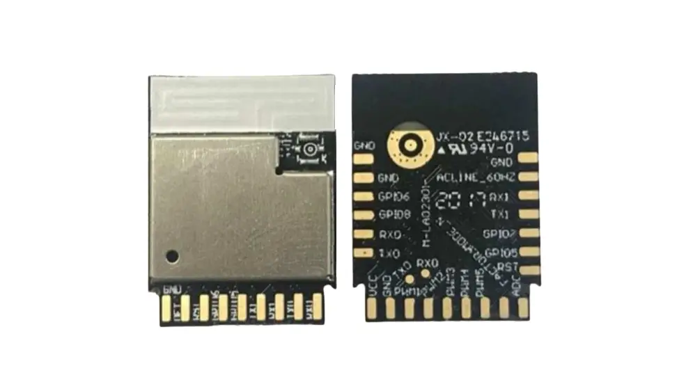
The LA02301 is a Leedarson-developed universal Wi-Fi and Bluetooth SMART (BLE) combo module. It uses the Espress if Inc. ESP32-U4WDH System in Package that integrates an embedded 4MB flash.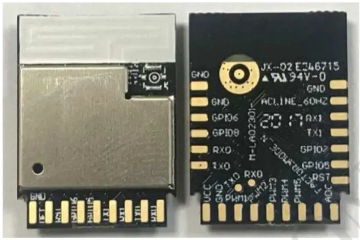
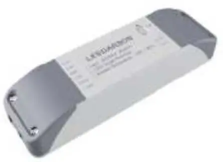
Figure 1.1. LA02301 Module
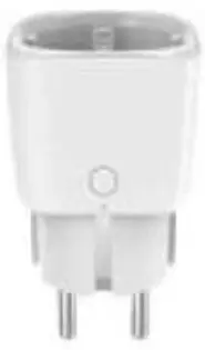
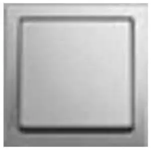
The LA02301 module is designed for a variety of IOT products such as Power Drivers, Sensors, Plugs, Lighting, Switches, etc.
- Plug

- Switch

- Sensor

- Down Light

- Power Driver

Figure 1.2. Product Application


Key features
- Embedded Xtensa® 32-bit LX6 microprocessor, with clock up to 160MHz
- Data Memory: 520KB internal SRAM and 448KB internal ROM,4MB Flash
- Power supply voltage: 3.0V 3.6V
- Operating temperature: -40 105 Deg-C
- Frequency of crystal oscillator: 40MHz\32.768KHz
- Operating frequency: 2400 2483.5MHz
- Support WIFI 802.11b/g/n up to 150Mbps Compliant with Bluetooth LE specifications Wi-Fi 802.11 b/g/n and BLE can’t transmission simultaneous
- Interface:
- Vertical Mount (Plug-In)
- 5 PWMs (GPlOs)
- 2 GPlOs
- 1 Available UART
- 1 ADC
- 1 Dedicated Triac Dimmer Detection Pin
- Horizontal (SMD)
- 5 PWMs (GPlOs)
- 4 GPlOs
- 1 Available UART
- 1 ADC
- 1 Dedicated Triac Dimmer Detection Pin
- Vertical Mount (Plug-In)
Block Diagram
The LA02301 module is a highly-integrated, high-performance system with all the hardware components needed to enable 2.4GHz wireless connectivity and support Wi-Fi and BLE protocols.
Built around the ESP32-U4WDH Wireless SoC, the LA02301 includes a built-in PCB trace antenna, supply decoupling and filtering components, a 40MHz reference crystal, a 32.768 KHz crystal, and an RF shield. A general block diagram of the module is shown as below.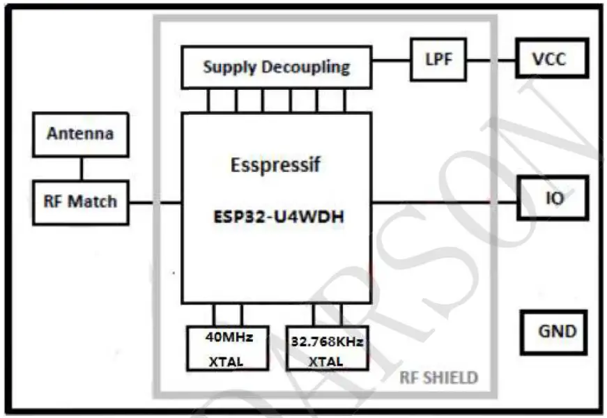
Figure1.3, LA02301 Block Diagram
Power Supply
The LA02301 requires a single nominal supply level of 3.3V. All the necessary decoupling and filtering components are included in the module. The supply voltage noise tolerance of the module should be less than 100mVpp and the supply current should be more than SOOmA.
Module Certification Information
Table 1.1. Module Certification Information
| Module | Certification Type | Certification Information |
LA02301 | FCC | 2AB2Q-LA02301 |
| IC | 10256A-LA02301 |
Electrical characteristics
Absolute maximum ratings
Stresses above those listed below may cause permanent damage to the device. This is a stress rating only and functional operation of the devices at those or any conditions above those indicated in the operation listing of this specification is not implied. Exposure to maximum rating conditions for extended periods may affect device reliability.
Table 2.1. Absolute maximum ratings
| Symbol | Parameter | Min. | Max. | Units | ||||
| VCC | Power Supply | -03 | ||||||
| GND | Ground of Module | |||||||
| VIO | Voltage of Module IO | -0.3 | +3.6 | V | ||||
| Storage temperature | -40 | +125 | Deg-C | |||||
| MSL | Moisture Sensitivity Level | |||||||
| ESD HBM | Human Body Mode | 1.5 | KV | |||||
| ESD CDM Charge Device Mode | 500 V | |||||||
General Operating Conditions
This table specifies the general operating temperature range and supply voltage range for all supplies, the minimum and maximum values of all other tables are specified over this operating range, unless otherwise noted.
Table 2.2. General Operating Conditions
Symbol | Parameter | Min. | Typ. | Max. | Units |
| VCC | Supply voltage, normal | 3.0 | 3.3 | 3.6 | V |
| TA | Operation temperature’ | -40 | 25 | 105 | Deg-C |
| ICCpeak | Supply Current Peak2 | 400 | 450 | mA | |
| ICC average | Suply Current average2 | 150 | mA | ||
Note:
| |||||
DC Specifications
Unless otherwise indicated, typical conditions are: VCC=3.3V.TA=25 Deg-C.
Table 2.3. DC Specifications
Symbol | Parameter(condition) | Min. | Typ. | Max. | Units |
| VIH | Input high voltage | 0.75xVCC | C112 | VCC | V |
| VIL | Input low voltage | GND | – | 0.25xVCC | V |
| VOH | Output high voltage | 0.8xVCC | – | – | V |
| VOL | Output low voltage | – | – | 0.1xVCC | V |
| IOH | Output high current | – | 40 | – | mA |
| IOL | Output low current | – | 28 | – | mA |
| RPU | Pull-up resistance | – | 45 | – | k Q |
| RPD | Pull-down resistance | – | 45 | – | k Q |
| ITX 802.11b peak | Transmit 1 lb DSSS 1Mbps Pout=+19dBm | – | 382 | mA | |
| ITX 802.11b average | Transmit llb DSSS 1Mbps Pout=+l9dBm | – | 148 | – | mA |
| ITX 802.11b peak | Transmit 11b DSSS 11Mbps Pout=+19dBm | – | 378 | – | mA |
| ITX 802.11b average | Transmit l lb DSSS 11Mbps Pout=+19dBm | – | 146 | – | mA |
| ITX 802.11g peak | Transmit l lg OFDM 6Mbps Pout=+l7dBm | – | 332 | – | mA |
| ITX 802.11g average | Transmit llg OFDM 6Mbps Pout=+l7dBm | – | 139 | – | mA |
| ITX 802.11g peak | Transmit l lg OFDM 54Mbps Pout=+13 dBm | – | 272 | – | mA |
| ITX 802.11g average | Transmit llg OFDM 54Mbps Pout=+13 dBm | – | 130 | – | mA |
| ITX 802.11n peak | Transmit 11n OFDM MCSO Pout=+17.5 dBm | – | 328 | mA | |
| ITX 802.11n average | Transmit lln OFDM MCSO Pout=+17.5 dBm | – | 140 | – | mA |
| ITX 802.11n peak | Transmit lln OFDM MCS7 Pout=+12 dBm | – | 256 | – | mA |
| ITX 802.11n average | Transmit lln OFDM MCS7 Pout=+12 dBm | – | 128 | – | ink |
| IRX 802.11b/g/n | Rx average current | – | 108 | – | mA |
| ITX BLE | Pout=8 dBm | – | 236 | – | mA |
| ITX BLE average | Pout=8 dBm | – | 184 | – | mA |
| IRX BLE | Rx average current | – | 115 | – | mA |
| Note: The current is measured with the module running the RF test Firmware @ | |||||
RF Specifications
Unless otherwise indicated, typical conditions are: VCC=3.3V TA=25 Deg-C,
Table 2.4. Wi-Fi Specifications
Symbol | Description | Min. | Typ. | Max. | Units |
| Fop | Operating frequencies | 2412 | – | 2484 | MHz |
| 1 lb DSSS 1Mbps output power | – | 19 | – | dBm | |
| PRF1 lb | |||||
| 1 lb DSSS 11Mbps output power | – | 19 | – | dBm | |
| 11g OFDM 6Mbps output power | – | 17 | – | dBm | |
| PRF11g | |||||
| 11g OFDM 54Mbps output power | – | 13 | – | dBm | |
| 11n OFDM HT20 MCSO output power | – | 17 | – | dBm | |
| 11n OFDM HT20 MCS7 output power | – | 12 | – | dBm | |
| PRF1 ln | |||||
| 11n OFDM HT40 MCSO output power | – | 16 | – | dBm | |
| 11n OFDM HT40 MCS7 output power | – | 11 | – | dBm | |
| Receiver sensitivity @1 lb DSSS 1Mbps | – | -95 | – | dBm | |
| Maximum receiving level @1 lb DSSS 1Mbps | – | 5 | – | dBm | |
| PSENS1 lb | |||||
| Receiver sensitivity @l lb DSSS 11Mbps | – | -86 | – | dBm | |
| Maximum receiving level @1 lb DSSS 11Mbps | – | 5 | – | dBm | |
| Receiver sensitivity @llg OFDM 6Mbps | – | -91 | – | dBm | |
| Maximum receiving level @llg OFDM 6Mbps | – | 0 | – | dBm | |
| PSENS11g | |||||
| Receiver sensitivity @11g OFDM 54Mbps | – | -73 | – | dBm | |
| Maximum receiving level @1 1 g OFDM 54Mbps | – | -8 | – | dBm | |
| Receiver sensitivity @l in OFDM HT20 MCSO | – | -90 | – | dBm | |
| Maximum receiving level @11n OFDM HT20 MCSO | – | 0 | – | dBm | |
| Receiver sensitivity @l In OFDM HT20 MCS7 | – | -71 | – | dBm | |
| Maximum receiving level @l In OFDM HT20 MCS7 | – | -8 | – | dBm | |
| PSENS1 in | |||||
| Receiver sensitivity @l In OFDM HT40 MCSO | – | -88 | – | dBm | |
| Maximum receiving level @l In OFDM HT40 MCSO | – | 0 | – | dBm | |
| Receiver sensitivity @l In OFDM HT40 MCS7 | – | -68 | – | dBm | |
| Maximum receiving level @l In OFDM HT40 MCS7 | – | -8 | – | dBm |
Table 2.5 BLE Specifications
Symbol | Description | Min. | Typ. | Max. | Units |
| Fop | Operating frequencies | 2402 | – | 2480 | MHz |
| LE Output Power | – | 8 | – | dBm | |
| PRFLE | LE Out Power Control range | – | 24 | – | dB |
| LE Out Power Control step | – | 3 | – | dB | |
| LE Receiver sensitivity | – | -90 | – | dBm | |
| PSENSLE | |||||
| LE Maximum receiving level | – | 0 | – | dBm |
Pin Definition
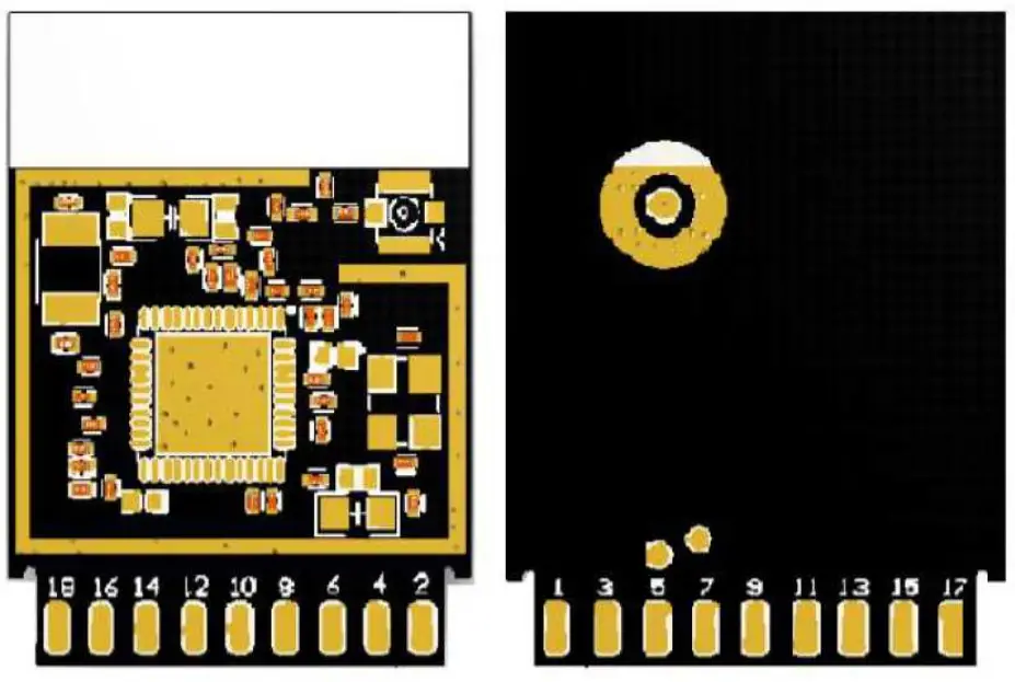
Figure 3.1. Vertical Mount (Plug-In)
Table 3.1. Plug-In pin definition
| Module No | *Pin of IC | Pin Definition | Pin Function Description | Direction |
| 1 | 1,3,4,19,26,37,4 3,46 | VCC | Power Supply | — |
| 2 | 40UORXD | RXO | FACTORY_UART_RX data in (RX) ground of module | I |
| 3 | 49 | GND | — | |
| 4 | 41 | TX0 | FACTORY_UART_TX data out (TX) | 0 |
| 5 | 17_MTMS | PWM1/I00 | PWM channel 1 output / GPIO 0 | I/O |
| 6 | 14_GPI025 | RX1 | HOST_UART_TX (data in to ESP32) , need | I |
| an external pull up | ||||
| 7 | 15_GPI026 | PWM2/I01 | PWM channel 2 output / GPIO 1 | I/O |
| 8 | 16_GPI027 | TX1 | HOSTUART_RX (data out from ESP32) , need an external pull up | 0 |
| 9 | 20_MTCK | PWM3/IO2 | PWM channel 3 output / GPIO 2 | I/O |
| 10 | 23 | 105 | GPIO 5 and BM SEL for UART boot; Default: weak pull up | I/O |
| 11 | 21_MTDO | PWM4/103 | PWM Channel 4 output / GPIO 3; Default: weak pull up | I/O |
| 12 | 36_GPI023 | 106 | GPIO6 | I/O |
| 13 | 24_GPIO4 | PWM5/I04 | PWM Channel 5 output / GPIO 4; Default: weak pull down | I/O |
| 14 | 9_CHIP_PU | /Reset | Reset, Low Active | I |
| 15 | 10_VDET_1 | FACTORY MODE | FACTORY MODE enable, low active | I |
| 16 | 1 l_VDET_2 | AC_TRIAC_DETEC T1 | Triac Dimmer Detect 0 – VCC (0 – 3.3V) | I |
| 17 | 5_SENSOR_VP | ADC | Analog-to-Digital Converter | I |
| 18 | 49 | GND | ground of module | — |
Note: 1. AC_TRIAC_DETECT is used to detect if a device is powered through a triac dimmer and to determine the dimmer settings. The circuit that feeds this signal should give a scaled DC voltage representation of the average AC voltage integrated over approximately 200ms. If the triac is set to chop the AC waveform 50%, the AC_TRIAC_DETECT signal should be at 50% of VCC.If the triac dimmer is turned up completely, the AC waveform will be minimally chopped and the AC_TRIAC_DETECT signal should be at 100% of VCC.
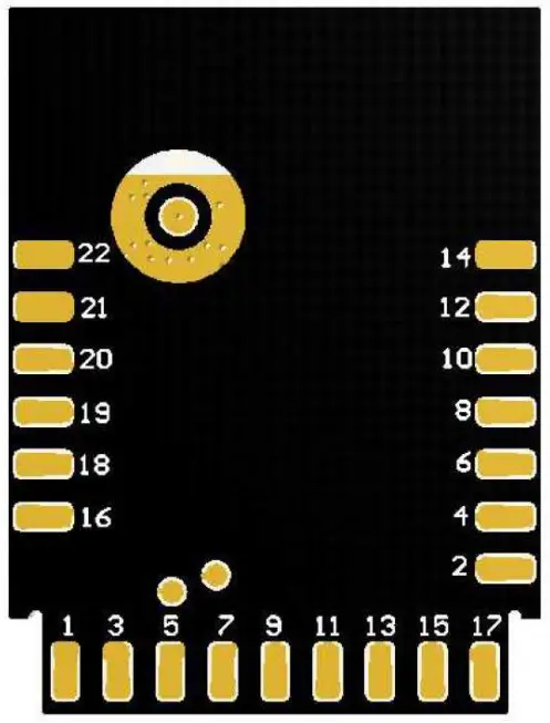
Figure 3.2. Horizontal (SMD)
Table 3.2. SMD pin definition
| Module No | Pin of IC Ai a | Pin Definition | Pin Function Description | Direction | |||||
| 1 | 1,3,4,19,26,37,43, 46 | VCC | Power Supply | — | |||||
| 2 | 9_CHIP_PU | /Reset | Reset, low active | I | |||||
| 3 | GND | GND | ground of module | — | |||||
| 4 | 23_GPIOO | 105 | GPIO 5 and BM_SEL for UART boot; Default: weak pull up | I/O | |||||
| 5 | 17_MTMS | PWMI/100 | PWM channel 1 output / GPIO 0 | I/O | |||||
| 6 | 35GP1018 | 107 | GPIO7 | I/O | |||||
| 7 | 15_GPIO26 | PWM2/101 | PWM channel 2 output / GPIO 1 | I/O | |||||
| 8 | 16_GPIO27 | TX1 | HOST_UART_RX (data out from ESP32), need an external pull up | 0 | |||||
| 9 | 20_MTCK | PWM3/IO2 | PWM channel 3 output / GPIO 2 | I/O | |||||
| 9 | 20_MTCK | PWM3/IO2 | PWM channel 3 output / GPIO 2 | 1 0 | |||||
| 10 | 14_GPIO25 | RX1 | HOST_UART_TX (data in to ESP32), need an external pull up | I | |||||
| 11 | 21_MTDO | PWM4/I03 | PWM channel 4 output / GPIO 3 Default: weak pull up | I/O | |||||
| 12 | 1 l_VDET_2 | AC_TRIAC_DETEC Ti | Triac Dimmer Detect 0 – VCC (0 – 3.3V) | 1 | |||||
| 13 | 24_013104 | PWM5/I04 | PWM Channel 5 output / GPIO 4; Default: weak pull down | 170 | |||||
| 14 | GND | GND | ground of module | — | |||||
| 15 | 10_VDET _1 | FACTORY_MODE_ N | FACTORY MODE enable, Low Active | 1 | |||||
| 16 | 41_UOTXD | TXO | FACTORY_UART_TX data out (TX) | 0 | |||||
| 17 | 5_SENSOR_VP | ADC | Analog-to-Digital Converter | I | |||||
| 18 | 40_UORXD | RXO | FACTORY_UART_RX data in (RX) | I | |||||
| I9 | 42_GPIO21 | 108 | GPIO8 | I/O | |||||
| 20 | 36_GPIO23 | 106 | GPIO6 | I/O | |||||
| 21 | GND | GND | ground of module | — | |||||
| 22 | GND | GND | ground of module | — | |||||
| Note: 1. AC_TRIAC_DETECT is used to detect if a device is powered through a triac dimmer and to determine the dimmer settings. The circuit that feeds this signal should give a scaled DC voltage representation of the average AC voltage integrated over approximately 200ms. If the triac is set to chop the AC waveform 50%, the AC_TRIAC_DETECT signal should be at 50% of VCC.If the triac dimmer is turned up completely, the AC waveform will be minimally chopped and the AC_TRIAC_DETECT signal should be at 100% of VCC. | |||||||||
Package Specifications
Dimension
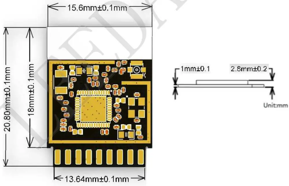
Figure 4.1. Module Dimensions (Unit: mm)
PCB Pads Information
Perspective view
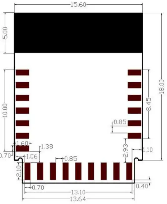
Figure 4.2. Pad Size (Unit: mm)
Note:
- Shaded part is Antenna Trace.
- The sizes of pads on the component side are the same to the opposite side.
Plug-in Land pattern example
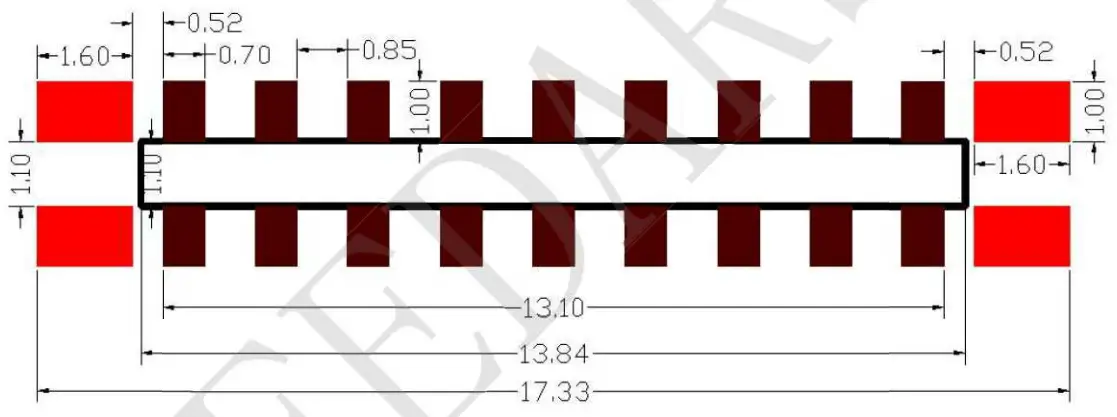
Figure 4.3. Plug-in PCB Land Pattern (Unit: mm)
Note:
Please see below lay-out:
Figure 4.4. Plug-in PCB Land Pattern (Unit: mm)
SMD Land pattern example
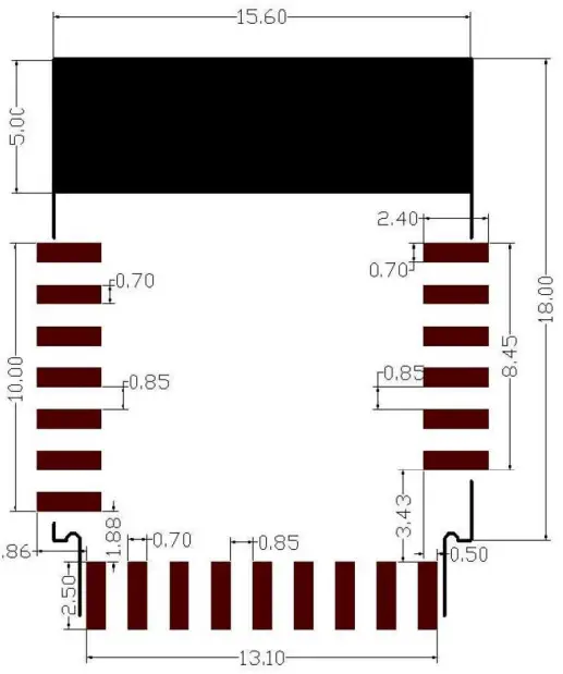
Figure 4.5. SMD PCB Land Pattern (Unit: mm)
Note:
Shaded part is Antenna Trace.
Soldering Recommendations
Refer to below information for SMT temperature settings. Note that the number of times of reflow should not above 2 times.
Table 5.1. SMT temperature setting
Set points(°C) | ||||||||||
| Zone | 1 | 2 | 3 | 4 | 5 | 6 | 7 | 8 | 9 | 10 |
| Top | 140 | 180 | 190 | 180 | 180 | 190 | 245 | 260 | 265 | 210 |
| Bottom | 140 | 180 | 190 | 180 | 180 | 190 | 245 | 260 | 265 | 210 |
| Conveyor Speed (cm/min):130.0 | ||||||||||
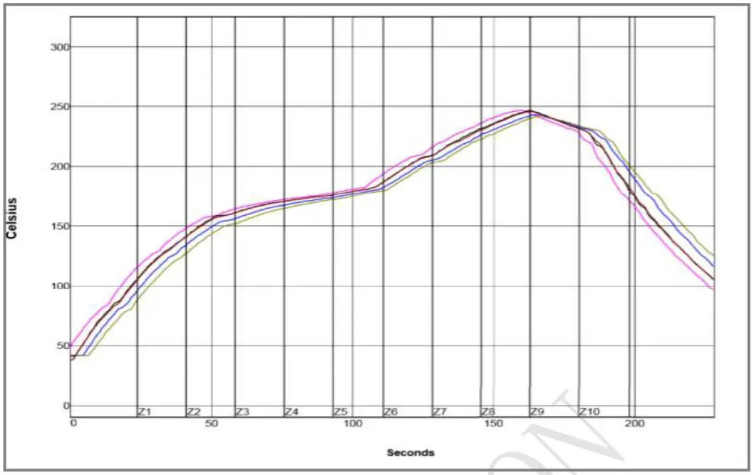
Figure 5.1. SMT temperature setting curve
Declaration
FCC Statement
This device complies with Part 15 of the FCC Rules. Operation is subject to the following two conditions: (1) This device may not cause harmful interference. (2) This device must accept any interference received, including interference that may cause undesired operation.
15.21
Note: The grantee is not responsible for any changes or modifications not expressly approved by the party responsible for compliance. Such modifications could void the user’s authority to operate the equipment.
15.105(b)
NOTE: This equipment has been tested and found to comply with the limits for a Class B digital device, pursuant to part 15 of the FCC Rules. These limits are designed to provide reasonable protection against harmful interference in a residential installation. This equipment generates uses and can radiate radio frequency energy and, if not installed and used in accordance with the instructions, may cause harmful interference to radio communications. However, there is no guarantee that interference will not occur in a particular installation. If this equipment does cause harmful interference to radio or television reception, which can be determined by turning the equipment off and on, the user is encouraged to try to correct the interference by one or more of the following measures:
- Reorient or relocate the receiving antenna.
- Increase the separation between the equipment and receiver.
- Connect the equipment into an outlet on a circuit different from that to which the receiver is connected.
- Consult the dealer or an experienced radio/TV technician for help
RF exposure Statement
This equipment complies with FCC radiation exposure limits set forth for an uncontrolled environment. This equipment should be installed and operated with minimum distance of 20 cm between the radiator and your body.
This device contains licence-exempt transmitter(s)/receiver(s) that comply with Innovation, Science and Economic Development Canada’s licence-exempt RSS(s). Operation is subject to the following two Condition.
- This device may not cause interference.
- This device must accept any interference, including interference that may cause undesired operation of the device.
Host labeling requirement:”Contains transmitter module
FCC ID: 2AB2Q-LA02301″ and IC: 10256A-LA02301


